EP1089450A2 - Telephone line interface circuit and method - Google Patents
Telephone line interface circuit and method Download PDFInfo
- Publication number
- EP1089450A2 EP1089450A2 EP00308181A EP00308181A EP1089450A2 EP 1089450 A2 EP1089450 A2 EP 1089450A2 EP 00308181 A EP00308181 A EP 00308181A EP 00308181 A EP00308181 A EP 00308181A EP 1089450 A2 EP1089450 A2 EP 1089450A2
- Authority
- EP
- European Patent Office
- Prior art keywords
- circuit
- line
- transmitter
- receiver
- output
- Prior art date
- Legal status (The legal status is an assumption and is not a legal conclusion. Google has not performed a legal analysis and makes no representation as to the accuracy of the status listed.)
- Granted
Links
Images


Classifications
-
- H—ELECTRICITY
- H04—ELECTRIC COMMUNICATION TECHNIQUE
- H04B—TRANSMISSION
- H04B1/00—Details of transmission systems, not covered by a single one of groups H04B3/00 - H04B13/00; Details of transmission systems not characterised by the medium used for transmission
- H04B1/38—Transceivers, i.e. devices in which transmitter and receiver form a structural unit and in which at least one part is used for functions of transmitting and receiving
- H04B1/40—Circuits
- H04B1/54—Circuits using the same frequency for two directions of communication
- H04B1/58—Hybrid arrangements, i.e. arrangements for transition from single-path two-direction transmission to single-direction transmission on each of two paths or vice versa
- H04B1/586—Hybrid arrangements, i.e. arrangements for transition from single-path two-direction transmission to single-direction transmission on each of two paths or vice versa using an electronic circuit
Definitions
- the present invention relates to an interface circuit for a telecommunications line, and particularly to a hybrid circuit for communicating over a telephone line.
- Hybrid circuits have been used in modems or other communication devices to isolate the modem receiver from being affected by transmissions of the modem transmitter.
- Known hybrid circuits include a transformer circuit utilizing at least two transformers. Although somewhat effective in isolating the modem receiver path from the modem transmitter path, the transformer hybrid circuit is expensive to implement on an integrated circuit.
- a second known hybrid circuit is a resistive divider circuit implemented in a resistor bridge configuration.
- the resistive divider circuit degrades the signal strength of the signal transmitted over the telecommunications line and itself generates an appreciable amount of thermal noise due to the presence of resistors therein, thereby providing a relatively poor signal-to-noise ratio. Consequently, for handling communication over a relative high loss line, such as a twisted pair telephone line, a resistive divider hybrid circuit is not a perfect solution.
- the present invention overcomes the shortcomings in prior systems and thereby satisfies a significant need for a hybrid circuit for a modem or other device having a transmitter and a receiver associated with a telecommunications line, such as a telephone line on which information is communicated in two directions using the ADSL protocol.
- the hybrid circuit substantially cancels signals generated by the modem transmitter from appearing at the input of the modem receiver and filters signals, such as echo signals, at unwanted frequencies so that the receiver primarily receives at its input signals transmitted from a remote device.
- the hybrid circuit includes a capacitive divider which suitably scales the signals generated by the transmitter and the signals appearing on the telecommunications line so that common portions of the two scaled signals substantially cancel each other at the receiver input.
- the capacitive divider is configured as a filter so that signal components at unwanted frequencies are substantially filtered from appearing at the receiver input.
- the capacitive divider is configured as a high pass filter.
- the hybrid circuit is associated with a differential pair of telecommunication lines over which information is communicated.
- the transmitter includes a differential output and the receiver includes a differential input.
- the hybrid circuit includes a pair of capacitive dividers, each of which is configured as a filter.
- each filter circuit is configured as a high pass filter.
- each filter circuit is configured as a low pass filter.
- the hybrid circuit is associated with a single ended telecommunications line. Accordingly, the transmitter output and the receiver input are each single ended.
- the hybrid circuit in this embodiment includes a single capacitive divider configured as a filter. In use in receiving downlink information from a remote device over the telecommunications line using ADSL, the capacitive divider forms a high pass filter. Conversely, in receiving uplink information from a remote device over an ADSL telecommunications line, the capacitive divider forms a low pass filter.
- the hybrid circuit is connected between the transmitter output, receiver input and the telecommunications line. An inverting amplifier is connected between the transmitter output and one terminal of the capacitive divider so as to generate a signal that, after being suitably scaled by the capacitive divider, cancels like signal components appearing on the telecommunications line.
- Hybrid circuit 1 is coupled to one end of a telecommunications line 2 over which information is communicated.
- Hybrid circuit 1 cooperates with transmitter 3 and receiver 4, each of which is coupled to telecommunications line 2.
- Transmitter 3 and receiver 4 respectively transmit and receive information over telecommunications line 2.
- hybrid circuit 1, transmitter 3 and receiver 4 may together form a modem or portion thereof.
- hybrid circuit 1 may be a stand-alone device.
- hybrid circuit 1 is electrically connected to transmitter 3, receiver 4 and telecommunication line 2 to substantially isolate the input of receiver 4 from signals generated by transmitter 3.
- Hybrid circuit 1 isolates the input of receiver 4 in part by canceling common signals appearing at the output of transmitter 3 and on telecommunications line 2. The remaining signal, a signal transmitted over telecommunications line 2 from a remote device, is applied to the input of receiver 4 for subsequent conditioning.
- hybrid circuit 1 is adapted for use with a two-wire telecommunications line 2.
- transmitter 3 has a differential output generated by transmitter elements 3A and 3B
- receiver 4 has a differential input that feeds receiver elements 4A and 4B.
- Transmitter element 3A is coupled to receiver element 4A and to telecommunications line 2A.
- transmitter element 3B is coupled to receiver element 4B and to telecommunications line 2B.
- Transmitter elements 3A and 3B are each associated with an output resistor Rout.
- hybrid circuit 1 includes a pair of circuits.
- First circuit 5 is connected to a telecommunications line 2A, an output of transmitter element 3B and an input to receiver element 4A.
- First circuit 5 is a capacitive divider including a first capacitor 6 having a first terminal connected to telecommunications line 2A and a second terminal, a second capacitor 7 having a first terminal connected to the output of transmitter element 3B and a second terminal that is connected to the second terminal of capacitor 6, and a pull-down device 8 connected between the input of receiver 4A and ground.
- capacitors 6 and 7 are chosen so that common signals between the output of transmitter element 3B and signals appearing on telecommunications line 2A are scaled relative to each other so as to be substantial inversions of each other. Because the two scaled signals are added together at the input of receiver element 4A, the two scaled signals are substantially canceled thereat.
- the voltage level of the signal generated by transmitter element 3B is twice the voltage level of the related signal appearing at telecommunications line 2A.
- the output signal generated by transmitter element 3B is scaled by one third (1/3) at the input of receiver 4A and the corresponding signal appearing on transmission line 2A is scaled by two thirds (2/3) thereat.
- these signals cancel each other at the input of receiver element 4A.
- the resulting signal appearing at the input of receiver element 4A is a portion of the differential signal transmitted to receiver 4 by a remote transmitter.
- the capacitive divider of first circuit 5 is configured as a filter for filtering signal components at unwanted frequencies (uplink or downlink) from appearing at the input of receiver element 4A.
- first circuit 5 is configured as a high pass filter.
- pull-down device 8 is a resistor having a resistance value that, when combined with capacitors 6 and 7, substantially filters ADSL uplink signals transmitted by transmitter 3.
- hybrid circuit 1 further includes a second circuit 12 which is electrically connected to telecommunications line 2B, the output of transmitter element 3A and the input of receiver element 4B.
- Second circuit 12 preferably mirrors first circuit 5 so as to correspondingly scale the output of transmitter element 3A and the related signal appearing on telecommunications line 2B relative to each other. In this way, the scaled signals cancel each other at the input to receiver element 4B so that receiver element 4B only receives signals transmitted by a remote transmitting device.
- second circuit 12 is implemented as a capacitive divider in order to suitably scale the signals for cancellation.
- Second circuit 12 preferably includes capacitor 13 having a first terminal connected to telecommunications line 2B and a second terminal, and capacitor 14 having a first terminal connected to the output of transmitter element 3A and a second terminal connected to the second terminal of capacitor 13.
- the capacitance values of capacitors 13 and 14 are chosen based upon the ratio of the signal voltage generated by transmitter element 3A to the signal voltage appearing on telecommunications line 2B due to the signal generated by transmitter element 3A.
- the capacitance values for capacitors 13 and 14 are chosen so that the ratio of the capacitance value of capacitor 13 to the capacitance value of capacitor 14 is the ratio of the voltage swing of the signal appearing at the output of transmitter element 3A to the voltage swing of the corresponding signal appearing on telecommunications line 2B. In this way, signals generated by transmitter 3A are substantially canceled at the input of receiver 4B.
- the capacitive divider of second circuit 12 is configured as a filter.
- second filter 12 is configured as a high pass filter to filter out uplink transmissions by transmitter element 3A.
- Resistor 15 of second circuit 12 is connected between the input of receiver element 4B and ground so as to cooperate with capacitors 13 and 14 in forming a high pass filter.
- hybrid circuit 31 for use with a single ended or one-wire telecommunications line.
- Hybrid circuit 31 is coupled to telecommunications line 32, the single ended output of transmitter 33, and the single ended input of receiver 34.
- Hybrid circuit 31 includes a capacitive divider circuit 35 for suitably scaling the output signal generated by transmitter 33 and the corresponding signal appearing on telecommunications line 32 so that they cancel each other at the input of receiver 34.
- capacitive divider circuit 35 includes a capacitor 36 having a first terminal connected to telecommunications line 32 and a second terminal, and capacitor 37 having a first terminal coupled to the output of transmitter 33 and a second terminal connected to the second terminal of capacitor 36.
- the capacitance values of capacitors 36 and 37 are chosen depending upon the ratio of the signal voltage generated by transmitter element 33 to the signal voltage appearing on telecommunications line 32 due to transmitter element 33.
- the capacitance values for capacitors 36 and 37 are chosen so that the ratio of the capacitance value of capacitor 36 to the capacitance value of capacitor 37 is the ratio of the voltage swing of the signal appearing at the output of transmitter element 33 to voltage swing of the corresponding signal voltage appearing on telecommunications line 32. In this way, signals generated by transmitter 33 are substantially canceled at the input of receiver 34.
- the capacitive divider of capacitive divider circuit 35 is configured as a filter.
- capacitive divider circuit 35 is configured as a high pass filter to filter out uplink transmissions.
- Resistor 38 of capacitive divider circuit 35 is connected between the input of receiver 34 and ground so as to cooperate with capacitors 36 and 37 in forming a high pass filter.
- hybrid circuit 31 is associated with a single ended telecommunications line 32, in order for the signals scaled by hybrid circuit 31 to cancel at the input of receiver 34, hybrid circuit 31 further includes an amplifier circuit 39 having an input connected to the output of transmitter 33 and an output connected to the first terminal of capacitor 37.
- Amplifier circuit 39 is configured as an inverting amplifier. Amplifier circuit 39 inverts the voltage level of the output of transmitter 33 so as to produce an inverted voltage level which, following scaling by capacitive circuit 35, cancels the corresponding signal appearing on telecommunications line 32 that itself was scaled by capacitive circuit 35. In this way, the contribution of the signal appearing at the input of receiver 34 due to transmitter 33 is substantially minimized
- a benefit of employing reactive elements in the divider of the present hybrid circuit to scale the signals for cancellation is that, unlike circuits utilizing resistive elements to scale signals, reactive elements do not generate an appreciable amount of thermal noise. As a result, the signal-to-noise ratio of the receive path of the present modem is not adversely affected by the present hybrid circuit. Further, because the capacitive divider circuit of the present hybrid circuit is configured as a filter, any thermal noise generated by the resistive element therein is suitably filtered.
- the receiving path for a modem or other communications device requires at least a third order filter.
- the filter(s) in the receiving path are normally downstream of an amplifier stage.
- hybrid circuit 1 as a first order high pass filter which is positioned upstream of the amplifier stage ( Figure 1), the filtering that is necessary downstream of the amplifier stage advantageously requires less complexity and can be implemented as an active filter implemented on an integrated circuit instead of an off-chip passive filter implemented using discrete L-C components.
- the present invention may be associated with a modem or other device including a transmitter for transmitting downlink information and a receiver for receiving uplink information at a different frequency range from the frequency range utilized by the transmitter, such as an uplink modem using the ADSL protocol.
- the hybrid circuit includes at least one resistive divider that is configured as a low pass filter.
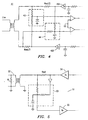
- Figure 4 illustrates a hybrid circuit 41 for an uplink modem or other device that communicates differential signals over telecommunications line 42 using ADSL.
- the primary difference between hybrid circuit 41 of Figure 4 and hybrid circuit 1 of Figure 2 is that each of first circuit 43 and second circuit 44 of hybrid circuit 41 is a resistive divider that is configured as a low pass filter via connection with a capacitor.
- First and second circuits being each configured as low pass filters suitably filters the higher frequency downlink transmissions by transmitter elements 45A and 45B.
- Figure 5 illustrates a hybrid circuit 51 for an uplink modem or other device that communicates single ended signals over telecommunications line 52 using ADSL.
- the scaling circuit 53 is a resistive voltage divider that is configured as a low pass filter via connection with a capacitor. In this way, circuit 53 suitably filters the higher frequency downlink transmissions by transmitter element so that only uplink information transmitted by a remote device is received at the input to receiver 55.
- a higher order filter either passive or active and either low-pass or high-pass, can be used instead of the first order filters mentioned above with respect to the preferred embodiments of the present invention.
- either the first capacitor or resistor of the higher order filter will be split to form a voltage divider.
- transmission line transformer can be used instead of an amplifier, or the counterphase signal tapped from the differential transmission line driver circuits (transmitter elements) to generate a counterphase voltage for subsequent signal cancellation in the hybrid circuit described above.
Landscapes
- Engineering & Computer Science (AREA)
- Computer Networks & Wireless Communication (AREA)
- Signal Processing (AREA)
- Cable Transmission Systems, Equalization Of Radio And Reduction Of Echo (AREA)
- Telephonic Communication Services (AREA)
- Dc Digital Transmission (AREA)
- Telephone Function (AREA)
- Networks Using Active Elements (AREA)
Abstract
Description
Claims (28)
- A device for transmitting and receiving signals over a communications line, comprising:a transmitter circuit having an output coupled to the communications line;a receiver circuit having an input coupled to the communications line; anda hybrid circuit connected to the transmitter output, the receiver input and the communications line, for filtering signals at frequencies that fall outside of a predetermined frequency range, the hybrid circuit being configured as a voltage divider formed from reactive elements for substantially canceling signals transmitted by the transmitter circuit from appearing at the receiver input.
- The device of claim 1, wherein:the hybrid circuit comprises a first order filter.
- The device of claim 1, wherein:the hybrid circuit comprises a high pass filter.
- The device of claim 1, wherein:the hybrid circuit is configured as a capacitive divider for scaling the signals at the transmitter output for cancellation with related signals appearing on the communications line.
- The device of claim 4, wherein the hybrid circuit comprises:a first capacitor having a first terminal connected to the communications line and a second terminal;a second capacitor having a first terminal connected to the transmitter output and a second terminal connected to the second terminal of the first capacitor; anda resistor having a first terminal connected to the second terminal of the first capacitor and a second terminal connected to a reference voltage.
- The device of claim 5, wherein:the ratio between the capacitance of the first capacitor to the capacitance of the second capacitor is substantially the same as the ratio between the voltage level at the transmitter output to the voltage level of a related signal appearing on the communications line.
- The device of claim 1, wherein:the communications line comprises a differential pair of communications lines;the transmitter output is a differential output;the receiver input is a differential input; andthe hybrid circuit comprises a first filter circuit having a first terminal connected to a first line of the differential pair of communications lines, a second terminal connected to a first line of the differential output of the transmitter and a third terminal connected to a first line of the differential input of the receiver, the first filter circuit being configured as a voltage divider formed from reactive elements for substantially canceling signals transmitted by the transmitter and appearing on the first terminal of the differential output thereof from appearing at the first line of the differential input of the receiver.
- The device of claim 7, wherein:the hybrid circuit further comprises a second filter circuit having a first terminal connected to a second line of the differential pair of communications lines, a second terminal connected to a second line of the differential output of the transmitter and a third terminal connected to a second line of the differential input of the receiver, the second filter circuit being configured as a voltage divider formed from reactive elements for substantially canceling signals transmitted by the transmitter and appearing on the second terminal of the differential output thereof from appearing at the second line of the differential input of the receiver.
- The device of claim 8, wherein:the second filter circuit forms a capacitive divider.
- The device of claim 8, wherein:the second filter circuit comprises a pair of series connected capacitors connected between the second line of the differential pair of communications lines and the second line of the differential output of the transmitter, and a resistor having a first terminal connected to each of the capacitors and a second terminal connected to a reference voltage.
- The device of claim 8, wherein:the second filter circuit comprises a first order, high pass filter.
- The device of claim 8, wherein:the first filter circuit and the second filter circuit each comprise a first order high pass filter.
- The device of claim 7, wherein:the first filter circuit comprises a pair of series connected capacitors connected between the first line of the differential pair of communications lines and the second line of the differential output of the transmitter, and a resistor having a first terminal connected to each of the capacitors and a second terminal connected to a reference voltage.
- The device of claim 7, wherein:the hybrid circuit further comprises an amplifier circuit configured as an inverting amplifier that is connected between the transmitter output and the first filter circuit, the amplifier circuit and the first filter circuit generating a first scaled output voltage signal and a second scaled voltage signal which cancel each other at the receiver input.
- A hybrid circuit associated with an end of a telecommunications line to which a transmitter and a receiver are connected, comprising:a first circuit having a first terminal coupled to an output of the transmitter, a second terminal coupled to an input of the receiver and a third terminal coupled to the telecommunications line, for canceling signals transmitted by the transmitter from appearing at the receiver input and filtering signals at predetermined frequencies on the telecommunications line from appearing at the receiver input so that the receiver is substantially isolated from the transmitter, the first circuit forming a voltage divider of reactive elements that is configured as a filter.
- The hybrid circuit of claim 15, wherein:the first circuit capacitively scales signals appearing at the output of the transmitter and on the telecommunications line so as to substantially cancel common signals therebetween.
- The hybrid circuit of claim 15 or 16, wherein:the first circuit is configured as a high pass filter.
- The hybrid circuit of claim 16, wherein the first circuit comprises:a first capacitor having a first terminal connected to the telecommunications line and a second terminal;a second capacitor having a first terminal connected to the transmitter output and a second terminal connected to the second terminal of the first capacitor; anda resistor connected between to the second terminal of the first capacitor and a reference voltage.
- The hybrid circuit of claim 18, wherein:the ratio between the capacitance value of the first capacitor to the capacitance value of the second capacitor is substantially the same as the voltage swing of signals at the transmitter output to the voltage swing of related signals appearing on the telecommunications line.
- The hybrid circuit of claim 15, further comprising:a second circuit configured as an inverting amplifier, the second circuit connected between the transmitter output and an input of the first circuit.
- The hybrid circuit of claim 15, wherein:the transmitter output is a differential output;the receiver input is a differential input;the telecommunications line is a two-wire line;the first terminal of the first circuit is connected to a first output line of the transmitter output, the second terminal of the first circuit is connected to a first input line of the receiver, and the third terminal of the first circuit is connected to a first line of the telecommunications line; andthe hybrid circuit further comprises a second circuit having a first terminal connected to a second output line of the transmitter output, a second terminal connected to a second input line of the receiver, and a third terminal connected to a second line of the telecommunications line, for canceling signals relating to signals generated by the transmitter and appearing at the second input line of the receiver, and for filtering signals on the second telecommunications line at predetermined frequencies from appearing at the second input line of the receiver, the second circuit forming a voltage divider of reactive elements that is configured as a filter.
- The hybrid circuit of claim 21, wherein:the second circuit capacitively scales signals appearing at the second output line of the transmitter and signals appearing on the second telecommunications line so that common signals therebetween cancel at the second input of the receiver.
- A hybrid circuit associated with an end of a telecommunications line to which a transmitter and a receiver are connected, comprising:a first filter circuit connected to an output of the transmitter, the telecommunications line and an input of the receiver, for filtering signals at predetermined frequencies appearing on the transmitter output and the telecommunications line, scaling signals appearing on the transmitter output, and canceling the scaled signals at the receiver input with related signals appearing on the telecommunications line.
- The hybrid circuit of claim 23, wherein:the first filter circuit includes a first reactive component connected between the telecommunications line and the receiver input, a first electrical component connected between the transmitter output and the receiver input, and a second electrical component connected between the receiver input and a reference voltage.
- The circuit device of claim 7 or 23, wherein:the first filter circuit is configured as a capacitive divider.
-
- The hybrid circuit of claim 25, wherein:the first filter circuit includes a first capacitor connected to the transmitter output, a second capacitor connected to the telecommunications line and a resistor connected to the first and second capacitors.
- The hybrid circuit of claim 26, wherein:the ratio of the capacitance value of the first capacitor to the capacitance value of the second capacitor is substantially the same as the voltage swing of the signals appearing on the transmitter output to the voltage swing of the related signals appearing on the telecommunications line.
Applications Claiming Priority (2)
| Application Number | Priority Date | Filing Date | Title |
|---|---|---|---|
| US09/408,742 US7050574B1 (en) | 1999-09-30 | 1999-09-30 | Telephone line interface circuit and method |
| US408742 | 1999-09-30 |
Publications (3)
| Publication Number | Publication Date |
|---|---|
| EP1089450A2 true EP1089450A2 (en) | 2001-04-04 |
| EP1089450A3 EP1089450A3 (en) | 2004-02-04 |
| EP1089450B1 EP1089450B1 (en) | 2006-11-22 |
Family
ID=23617568
Family Applications (1)
| Application Number | Title | Priority Date | Filing Date |
|---|---|---|---|
| EP00308181A Expired - Lifetime EP1089450B1 (en) | 1999-09-30 | 2000-09-20 | Telephone line interface circuit |
Country Status (4)
| Country | Link |
|---|---|
| US (1) | US7050574B1 (en) |
| EP (1) | EP1089450B1 (en) |
| JP (1) | JP2001160868A (en) |
| DE (1) | DE60031934D1 (en) |
Cited By (1)
| Publication number | Priority date | Publication date | Assignee | Title |
|---|---|---|---|---|
| EP1829351A4 (en) * | 2004-12-02 | 2010-07-14 | Solarflare Comm Inc | INSULATION OF EMISSION AND RECEPTION SIGNALS |
Families Citing this family (3)
| Publication number | Priority date | Publication date | Assignee | Title |
|---|---|---|---|---|
| US7460662B2 (en) * | 2004-12-02 | 2008-12-02 | Solarflare Communications, Inc. | Isolation of transmit and receive signals in full-duplex communication systems |
| US8385538B2 (en) * | 2008-12-10 | 2013-02-26 | Utc Fire & Security Americas Corporation, Inc. | Method, system, and apparatus for a differential transformer-free hybrid circuit |
| US10484042B2 (en) * | 2018-03-09 | 2019-11-19 | Texas Instruments Incorporated | Bidirectional data link |
Family Cites Families (9)
| Publication number | Priority date | Publication date | Assignee | Title |
|---|---|---|---|---|
| US3934099A (en) | 1974-08-16 | 1976-01-20 | Bell Telephone Laboratories, Incorporated | Bias, feedback and network arrangements for hybrid circuits |
| US4278847A (en) * | 1979-02-26 | 1981-07-14 | Tii Corporation | Transformerless hybrid circuits |
| CA1157124A (en) * | 1981-11-18 | 1983-11-15 | David G. Agnew | Hybrid circuit including capacitive charge-transfer means |
| US4878241A (en) * | 1988-10-03 | 1989-10-31 | Da-Tel Research Company, Incorporated | Audio frequency interface for differential relays |
| US5734703A (en) * | 1993-05-26 | 1998-03-31 | Hitachi Maxell, Ltd. | Hybrid circuit and data communication apparatus |
| US5541990A (en) * | 1994-07-05 | 1996-07-30 | Rockwell International Corporation | Compensated hybrid |
| EP0739120B1 (en) | 1995-04-11 | 2001-06-06 | STMicroelectronics S.r.l. | Speech circuit for subscriber telephone apparatus |
| US5822426A (en) * | 1995-06-06 | 1998-10-13 | International Business Machines Corporation | Balanced hybrid circuit |
| WO1998010553A2 (en) * | 1996-09-02 | 1998-03-12 | Telia Ab (Publ) | Improvements in, or relating to, control channels for telecommunications transmission systems |
-
1999
- 1999-09-30 US US09/408,742 patent/US7050574B1/en not_active Expired - Lifetime
-
2000
- 2000-09-20 EP EP00308181A patent/EP1089450B1/en not_active Expired - Lifetime
- 2000-09-20 DE DE60031934T patent/DE60031934D1/en not_active Expired - Lifetime
- 2000-09-29 JP JP2000299402A patent/JP2001160868A/en active Pending
Cited By (1)
| Publication number | Priority date | Publication date | Assignee | Title |
|---|---|---|---|---|
| EP1829351A4 (en) * | 2004-12-02 | 2010-07-14 | Solarflare Comm Inc | INSULATION OF EMISSION AND RECEPTION SIGNALS |
Also Published As
| Publication number | Publication date |
|---|---|
| JP2001160868A (en) | 2001-06-12 |
| US7050574B1 (en) | 2006-05-23 |
| DE60031934D1 (en) | 2007-01-04 |
| EP1089450B1 (en) | 2006-11-22 |
| EP1089450A3 (en) | 2004-02-04 |
Similar Documents
| Publication | Publication Date | Title |
|---|---|---|
| CA2046250A1 (en) | Hybrid circuit having a two-wire/four-wire converting function | |
| EP1492287A1 (en) | Receiver | |
| US6804349B1 (en) | Hybrid transceiver circuit | |
| EP0635953B1 (en) | System for increasing the capacity of existing local area networks that use shielded twisted wire pair medium | |
| EP1241799B1 (en) | Hybrid circuit for a broadband modem | |
| US7194037B1 (en) | Active replica transformer hybrid | |
| US7050574B1 (en) | Telephone line interface circuit and method | |
| US5541990A (en) | Compensated hybrid | |
| CA2327209A1 (en) | Method and device for echo cancelling | |
| US7778210B2 (en) | Bridge circuit to suppress echoes in communication devices | |
| JP3630369B2 (en) | Analog echo filter | |
| EP2061158B1 (en) | Hybrid circuit without inductors | |
| US7020277B1 (en) | DSL line interface having low-pass filter characteristic with reduced external components | |
| US4288661A (en) | Interface circuitry for acoustic coupler compensation | |
| US4034166A (en) | Transmission networks for telephone system | |
| CN112929055B (en) | Echo cancellation circuit | |
| JPH10126817A (en) | 2-wire 4-wire conversion circuit | |
| US7330545B2 (en) | Dual transformer hybrid system and method | |
| JPH033009Y2 (en) | ||
| JP3023846U (en) | Out-of-band signal separation and superposition circuit | |
| JPS6042512Y2 (en) | high frequency attenuator | |
| EP0739120A1 (en) | Speech circuit for subscriber telephone apparatus | |
| JPH04369127A (en) | 2-wire 4-wire conversion circuit | |
| JPS6146629A (en) | Ac inducing noise eliminating circuit | |
| HK1132103B (en) | A hybrid circuit without an inductor |
Legal Events
| Date | Code | Title | Description |
|---|---|---|---|
| PUAI | Public reference made under article 153(3) epc to a published international application that has entered the european phase |
Free format text: ORIGINAL CODE: 0009012 |
|
| AK | Designated contracting states |
Kind code of ref document: A2 Designated state(s): AT BE CH CY DE DK ES FI FR GB GR IE IT LI LU MC NL PT SE |
|
| AX | Request for extension of the european patent |
Free format text: AL;LT;LV;MK;RO;SI |
|
| RIN1 | Information on inventor provided before grant (corrected) |
Inventor name: VARELJIAN, ALBERT |
|
| PUAL | Search report despatched |
Free format text: ORIGINAL CODE: 0009013 |
|
| AK | Designated contracting states |
Kind code of ref document: A3 Designated state(s): AT BE CH CY DE DK ES FI FR GB GR IE IT LI LU MC NL PT SE |
|
| AX | Request for extension of the european patent |
Extension state: AL LT LV MK RO SI |
|
| RIC1 | Information provided on ipc code assigned before grant |
Ipc: 7H 04B 1/58 A Ipc: 7H 04B 1/52 B |
|
| 17P | Request for examination filed |
Effective date: 20040729 |
|
| AKX | Designation fees paid |
Designated state(s): DE FR GB IT |
|
| 17Q | First examination report despatched |
Effective date: 20041020 |
|
| GRAP | Despatch of communication of intention to grant a patent |
Free format text: ORIGINAL CODE: EPIDOSNIGR1 |
|
| RTI1 | Title (correction) |
Free format text: TELEPHONE LINE INTERFACE CIRCUIT |
|
| GRAS | Grant fee paid |
Free format text: ORIGINAL CODE: EPIDOSNIGR3 |
|
| GRAA | (expected) grant |
Free format text: ORIGINAL CODE: 0009210 |
|
| AK | Designated contracting states |
Kind code of ref document: B1 Designated state(s): DE FR GB IT |
|
| PG25 | Lapsed in a contracting state [announced via postgrant information from national office to epo] |
Ref country code: IT Free format text: LAPSE BECAUSE OF FAILURE TO SUBMIT A TRANSLATION OF THE DESCRIPTION OR TO PAY THE FEE WITHIN THE PRESCRIBED TIME-LIMIT;WARNING: LAPSES OF ITALIAN PATENTS WITH EFFECTIVE DATE BEFORE 2007 MAY HAVE OCCURRED AT ANY TIME BEFORE 2007. THE CORRECT EFFECTIVE DATE MAY BE DIFFERENT FROM THE ONE RECORDED. Effective date: 20061122 |
|
| REG | Reference to a national code |
Ref country code: GB Ref legal event code: FG4D |
|
| REF | Corresponds to: |
Ref document number: 60031934 Country of ref document: DE Date of ref document: 20070104 Kind code of ref document: P |
|
| PG25 | Lapsed in a contracting state [announced via postgrant information from national office to epo] |
Ref country code: DE Free format text: LAPSE BECAUSE OF FAILURE TO SUBMIT A TRANSLATION OF THE DESCRIPTION OR TO PAY THE FEE WITHIN THE PRESCRIBED TIME-LIMIT Effective date: 20070223 |
|
| ET | Fr: translation filed | ||
| RIN2 | Information on inventor provided after grant (corrected) |
Inventor name: VARELJIAN, ALBERT |
|
| PLBE | No opposition filed within time limit |
Free format text: ORIGINAL CODE: 0009261 |
|
| STAA | Information on the status of an ep patent application or granted ep patent |
Free format text: STATUS: NO OPPOSITION FILED WITHIN TIME LIMIT |
|
| 26N | No opposition filed |
Effective date: 20070823 |
|
| PGFP | Annual fee paid to national office [announced via postgrant information from national office to epo] |
Ref country code: FR Payment date: 20080915 Year of fee payment: 9 |
|
| PGFP | Annual fee paid to national office [announced via postgrant information from national office to epo] |
Ref country code: GB Payment date: 20080924 Year of fee payment: 9 |
|
| GBPC | Gb: european patent ceased through non-payment of renewal fee |
Effective date: 20090920 |
|
| REG | Reference to a national code |
Ref country code: FR Ref legal event code: ST Effective date: 20100531 |
|
| PG25 | Lapsed in a contracting state [announced via postgrant information from national office to epo] |
Ref country code: FR Free format text: LAPSE BECAUSE OF NON-PAYMENT OF DUE FEES Effective date: 20090930 |
|
| PG25 | Lapsed in a contracting state [announced via postgrant information from national office to epo] |
Ref country code: GB Free format text: LAPSE BECAUSE OF NON-PAYMENT OF DUE FEES Effective date: 20090920 |