EP1089435A2 - Phase shifter circuit and delay locked loop - Google Patents
Phase shifter circuit and delay locked loop Download PDFInfo
- Publication number
- EP1089435A2 EP1089435A2 EP00305349A EP00305349A EP1089435A2 EP 1089435 A2 EP1089435 A2 EP 1089435A2 EP 00305349 A EP00305349 A EP 00305349A EP 00305349 A EP00305349 A EP 00305349A EP 1089435 A2 EP1089435 A2 EP 1089435A2
- Authority
- EP
- European Patent Office
- Prior art keywords
- phase
- signal
- input signal
- phase shifter
- output
- Prior art date
- Legal status (The legal status is an assumption and is not a legal conclusion. Google has not performed a legal analysis and makes no representation as to the accuracy of the status listed.)
- Withdrawn
Links
Images





Classifications
-
- H—ELECTRICITY
- H03—ELECTRONIC CIRCUITRY
- H03K—PULSE TECHNIQUE
- H03K5/00—Manipulating of pulses not covered by one of the other main groups of this subclass
- H03K5/13—Arrangements having a single output and transforming input signals into pulses delivered at desired time intervals
- H03K5/133—Arrangements having a single output and transforming input signals into pulses delivered at desired time intervals using a chain of active delay devices
-
- H—ELECTRICITY
- H03—ELECTRONIC CIRCUITRY
- H03L—AUTOMATIC CONTROL, STARTING, SYNCHRONISATION OR STABILISATION OF GENERATORS OF ELECTRONIC OSCILLATIONS OR PULSES
- H03L7/00—Automatic control of frequency or phase; Synchronisation
- H03L7/06—Automatic control of frequency or phase; Synchronisation using a reference signal applied to a frequency- or phase-locked loop
- H03L7/08—Details of the phase-locked loop
- H03L7/081—Details of the phase-locked loop provided with an additional controlled phase shifter
- H03L7/0812—Details of the phase-locked loop provided with an additional controlled phase shifter and where no voltage or current controlled oscillator is used
- H03L7/0816—Details of the phase-locked loop provided with an additional controlled phase shifter and where no voltage or current controlled oscillator is used the controlled phase shifter and the frequency- or phase-detection arrangement being connected to a common input
-
- H—ELECTRICITY
- H03—ELECTRONIC CIRCUITRY
- H03K—PULSE TECHNIQUE
- H03K5/00—Manipulating of pulses not covered by one of the other main groups of this subclass
- H03K2005/00013—Delay, i.e. output pulse is delayed after input pulse and pulse length of output pulse is dependent on pulse length of input pulse
- H03K2005/00019—Variable delay
-
- H—ELECTRICITY
- H03—ELECTRONIC CIRCUITRY
- H03K—PULSE TECHNIQUE
- H03K5/00—Manipulating of pulses not covered by one of the other main groups of this subclass
- H03K2005/00286—Phase shifter, i.e. the delay between the output and input pulse is dependent on the frequency, and such that a phase difference is obtained independent of the frequency
Definitions
- This invention relates to a method and apparatus for enabling unlimited phase tracking in high speed data synchronisation, for example in telecommunications equipment.
- the invention relates in particular to a delay locked loop which provides continuous, precise alignment of two signals in excess of one signal period.
- the invention also relates to a phase shifter circuit which provides phase shifting over more than one signal period.
- a delay locked loop which is a type of phase locked loop, uses a phase detector to generate an error voltage proportional to the phase difference between two input signals. The error voltage is, in turn used to control a phase shifter which adjusts the delay, or phase, of one of the signals to achieve phase alignment of the two signals.
- phase shifter which adjusts the delay, or phase, of one of the signals to achieve phase alignment of the two signals.
- An alternative approach may be to operate the loop at a submultiple frequency of the signals being tracked.
- the disadvantage of this approach is that the original frequency needs to be recovered before the output signals can be used. This process introduces further errors and complications into the circuitry.
- a phase shifter reset circuit for phase shifting an input signal, having an input and an output, comprising:
- a phase shifter to provide a continuously phase shifted output signal comprising:
- a delay locked loop having an output for generating an output signal and a second input for receiving a delayed version of output signal, for inserting a delay representative of the delay inserted into the output signal into the output signal comprising:
- a delay into an input signal to produce an output signal said delay being representative of a delay inserted into delayed version of the output signal, comprising:
- the phase shift reference signal may be generated by a phase detector device and may thus represent the difference between two signals which require phase, or delay, alignment.
- the phase shifter reset circuit and method may form an integral part of a delay locked loop.
- the output signal is, according to the invention, maintained throughout the range of possible phase shifts and allows the phase shifter to be reset and to stabilise without affecting the output signal. By temporarily by-passing the phase shifter, the integrity of the output signal is maintained through the reset process, thereby enabling the phase shifter circuit to track phase shifts of more than one period.
- the phase shifter circuit of the invention is considerably more reliable than those of the prior art because it is not limited to the traditional 360° range.
- Figure 1 shows a plot of control voltage (i.e. phase shift reference signal voltage) against phase output for a known phase shifter.
- control voltage i.e. phase shift reference signal voltage
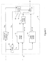
- FIG. 2 shows in outline a continuous phase shifter circuit (10) according to the invention.
- the phase of an input signal (i/p) is shifted by phase shifter (12) by an amount set by the phase shift reference signal voltage (V ⁇ r ).
- the voltage level of the phase shift reference signal is also continuously monitored by a threshold detector circuit (14).
- a fixed phase shifter (16) which introduces a predetermined phase shift into the input signal.
- This predetermined phase shift is set to be similar to the threshold phase shift Voltage (V a of Figure 1), that is, that phase shift produced at point "a" (just before the phase shifter becomes unreliable).
- the phase shift of the fixed phase shift may be 180o (that is an inversion of the input signal) and the threshold is thus V 1 (equivalent to 180o).
- the threshold detector circuit is set to a threshold value (V a ) and detects a control voltage which would introduce phase shift from the phase shifter also of ⁇ a .
- V SW switching signal
- the bypass circuit comprises a simple switch (20) and a simple timer and control logic (22) which generates a trigger signal (V TR ).
- the switch is normally set to pass the phase shift input signal (i/p + ⁇ r ) as its output.
- the switch When prompted by the switching signal, the switch passes, in place of the phase shifted input signal, the fixed phase shifted input signal (i/p + ⁇ f ) as its output.
- the switch remains engaged for a predetermined period, sufficiently long enough for the control logic to generate the trigger signal to reset the phase shifter via reset logic (24).
- the phase shifter is reset to point "d" and allowed to settle before the switch switches back to passing the phase shifted input signal as its output.
- FIG 3 shows an alternative embodiment of the phase shifter including a phase invertor (26).
- the phase shifter (12) is reset to point b and the phase of the phase shifter is inverted by phase invertor (26) to maintain the phase of the circuit output signal.
- the advantage of this embodiment is that the start up position and the reset position can be the same; with the embodiment illustrated in Figure 2, the reset position is dependent upon the threshold point reached by the phase shifter circuit (that is point a is reset to point d and point c is reset to point b). This requires more complex reset circuitry.
- phase shifter (16) may be replaced by a phase invertor which introduces a phase shifter of 180o in the input signal.
- the bypass process is initiated when the required phase shift is also 180o.
- the advantage of this approach is that during the bypass the phase shifter may be reset to zero, which requires simpler circuitry than the offset devices described above.
- Figure 4 shows the operation of signals produced by the circuits of Figures 2 & 3 and assumes a threshold voltage of V 1 (i.e. 180o).
- V 1 i.e. 180o
- the switching signal V sw is generated, during which time the output is switched from the phase shifted input signal to the fixed phase shifted input signal.
- the timing diagram of Figure 4 is based on the assumption that the phase shift reference signal voltage gradually increases or decreases over time; such an assumption is valid it the reference signal drifts gradually from an initial standard e.g. due to a gradual temperature or humidity increase.
- the phase shift reference signal voltage V ⁇ r is not reset instantaneously when the control circuit generates the trigger voltage V TR to zero but decays over a period of time; the output is kept at the fixed phase shift signal until that decay is completed.
- FIG. 5 shows in outline a data frame and a data serializer which employ a delay locked loop (DLL 30).
- the DLL is used in a serializer circuit (32) to align the clock signal (34) received by the serializer with a clock signal employed by a framer (36), upstream from the serializer.
- the clock signal received by the framer may be out of phase, in absolute terms, with the clock signal received by the serializer.
- phase or delay offset between the clock signals employed by the two circuits may vary with time, temperature, humidity etc, assuming a fixed delay is not appropriate when data integrity needs to be maintained over a significant period e.g. several days.
- the internal and external delays may be unpredictable and may drift by several signal or clock periods during operation.
- the DLL thus measures the difference between the reference clock (34) employed in the serializer and the clock signal returned by the framer and generates an adjusted (i.e. phase shifted) clock signal to be used where necessary in the serializer.
- the action of the phase detector is to produce an output signal, which is a pulse stream whose duty cycle varies according to the phase difference between two input signals.
- This output signal is low pass filtered or integrated to produce a low frequency signal that varies according to the mean level of the pulse stream.
- This low frequency signal is then amplified to increase the sensitivity of the loop.
- the amplification and integration function may be combined using a high gain amplifier, which uses a capacitor as the feedback path.
- the phase detector characteristic is approximately linear with an abrupt change in output from maximum positive value to maximum negative value at typical phase values of +180° or -180°.
- the action of the DLL is to maintain edge alignment of the returned clock (38) with the reference clock (34) by adjusting the phase shifter (12) to produce a phase shifted clock signal (CLOCK OUT 40).
- the loop maintains lock as the phase delay introduced by the external path in the framer changes.
- the analogue phase shifter has a limited range of +/- 180°, as shown in Figure 1.
- the loop will loose lock, and data may thus be sampled and generated erroneously. Any change to the phase shift reference voltage V ⁇ r will have a delay dictated by the filter characteristics.
- the filter time constant may be 1000 times greater than the reference clock and during this time the clock out may be significantly out of alignment from the reference clock and/or the returned clock.
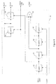
- Figure 7 shows in more detail a DLL according to the invention.
- the phase shifter is substituted by a fixed phase shifted version of the reference clock.
- the phase detector generates a difference signal by differencing the reference clock with the returned clock.
- the amplifier and filter circuit (24') functions as described above, in connection with Figure 5, to provide a reference signal V ⁇ r .
- the threshold detector (14) triggers at an amplitude equivalent to 180° phase shift of either polarity. This in turn triggers monostable (42), which has a period greater than the reset period of the loop filter and which in turn triggers the switch control (44).
- Switch B is activated to provide a signal 180° shifted from its previous output signal.
- the switch control activates switch C (20) to switch its output from the phase shifter (12) to the output of switch B (16').
- Switch B inserts a 180° fixed phase shift inverting the reference clock (i.e. the input signal) and is used as the fixed phase shifter.
- Switch A (26') is activated, having been previously isolated from the output by switch C.
- Switch A inverts the signal (equivalent to a 180° phase shift).
- the output voltage on the filter of the reset circuit (24') is then discharged to zero.
- This combination of zero phase shift from the phase shifter and the inversion of switch A again produces the same phase shift as before initiation of the reset sequence, but with the reference voltage V ⁇ r set again to zero.
- switch C is activated to return the output of the phase shifter as to the output signal source
- Figure 8 shows a block schematic of switch control (44) which is designed to take all timing from a rising clock edge. It is also designed such that all switch transitions occur on the falling clock edge, enabling all switching activity to be completed before the rising edge occurs and thereby giving a seamless reset cycle.
- the circuit shown in figure 8 may be used to generate the sequence of control signals to switches and filter reset functions.
- the sequence is illustrated in figure 9.
- the output of latch 3 (52) is used to enable and hold the filter reset circuit (24').
- Switch control latches 5 and 6 which control switches A and B respectively are toggled to their other state once in each reset cycle.
- the output of the OR gate (54) is used to control the state of switch C.
Landscapes
- Physics & Mathematics (AREA)
- Nonlinear Science (AREA)
- Stabilization Of Oscillater, Synchronisation, Frequency Synthesizers (AREA)
Abstract
Description
Claims (22)
- a phase shifter reset circuit, for phase shifting an input signal, having an input and an output, comprising:a phase shifter, having a first input for receiving said input signal, a second input for receiving a phase shift reference signal and an output for outputting a phase shifted input signal, wherein the phase of the input signal is shifted by a phase shifter determined by the phase shift reference signal;a resetter, for resetting the phase shift reference signal in response to a trigger signal;a fixed phase shifter, for shifting the phase of said input signal by a predetermined phase shift, connected in parallel with said phase shifter, having an input for receiving said input signal and an output for outputting a fixed phase shifted input signal;a threshold detector circuit, having an input for receiving said phase shift reference signal and an output for outputting a switching signal when said phase shift reference signal reaches a threshold level, substantially equivalent to the phase shift introduced into said input signal by the fixed phase shifter;a bypass circuit, disposed between said phase shifters and said output, having two inputs for receiving, respectively, said phase shifted input signal and said fixed phase shifted signal, a switch for selecting a selected signal from either said phase shifted input signal or said fixed phase shifted signal, an output for outputting said selected signal and means for generating said trigger signal, whereby said switch is responsive to said switching signal to switch from said phase shifted input signal to said fixed phase shifted signal for a predetermined period of time, during which time said trigger signal is generated, before switching back to said phase shifted input signal.
- A phase shifter reset circuit as claimed in Claim 1, wherein the resetter comprises an amplifier and a filter.
- A phase shifter reset circuit as claimed in Claim 1 or 2, wherein the fixed phase shifter inverts the input signal to provide the fixed phase shifted input signal.
- A phase shifter reset circuit as claimed in any proceeding claims, wherein the threshold level is set to a level representative of 180° phase shift from the phase shifter.
- A phase shifter reset circuit as claimed in any preceding claim wherein the bypass circuit comprises a timer circuit, a control logic and a switch.
- A phase shifter reset circuit as claimed in any preceding claim wherein said predetermined period of time is sufficient for said resetter to reset.
- A delay locked loop including a phase shifter reset circuit according to any preceding claim.
- A framer and a serializer combination including a delay locked loop according to Claim 7.
- A method of resetting a phase shifter to provide a continuously phase shifted output signal comprising:phase shifting, in a phase shifter, said input signal by a phase shift determined by a phase shift reference signal to produce a phase shifted input signal;resetting said phase shifter in response to a trigger signal;phase shifting, in a fixed phase shifter disposed in parallel with said phase shifter, said input signal by a predetermined fixed phase shift to produce a fixed phase shifted input signal;detecting in a threshold detector when said phase shift reference signal reaches a predetermined threshold level, equivalent to the phase shift introduced by said fixed phase shifter and generating in response a switching signal;switching at said output, in response to said switching signal, from said phase shifted input signal to said fixed phase shifted input signal for a predetermined period of time, during which time said trigger signal is generated, before switching back to said phase shifted input signal.
- A method as claimed in Claim 9, wherein the fixed phase shift is an inversion of the input signal.
- A method as claimed in Claim 9 or Claim 10, wherein the threshold is set to a level representative of 180° phase shift from the phase shifter.
- A method as claimed in Claim 9, 10 or 11, whereby the predetermined period of time is sufficient to reset said phase shifter.
- A delay locked loop for receiving an input signal, a delay locked loop, having an output for generating an output signal and a second input for receiving a delayed version of output signal, for inserting a delay representative of the delay inserted into the output signal into the output signal comprising:a phase detector, having a first input for receiving said input signal and a second input for receiving said delayed version of the output signal, for generating and outputting at an output a phase shift reference signal representative of the phase difference between said input signal and said delayed version of the output signal;a phase shifter, having a first input for receiving said input signal, a second input for receiving said phase shift reference signal and an output for outputting a phase shifted input signal, wherein the phase of the input signal is shifted by a phase shift determined by the phase shift reference signal;a resetter, for resetting the phase shift reference signal in response to a trigger signal;a fixed phase shifter, for shifting the phase of said input signal by a predetermined phase shift, connected in parallel with said phase shifter, having an input for receiving said input signal and an output for outputting a fixed phase shifted input signal;a threshold detector circuit, having an input for receiving said phase shift reference signal and an output for outputting a switching signal when said phase shift reference signal reaches a threshold level, substantially equivalent to the phase shift introduced into said input signal by the fixed phase shifter;a bypass circuit, disposed between said phase shifters and said output, having two inputs for receiving, respectively, said phase shifted input signal and said fixed phase shifted signal, a switch for selecting a selected signal from either said phase shifted input signal or said fixed phase shifted signal, an output for outputting said selected signal and means for generating said trigger signal, whereby said switch is responsive to said switching signal to switch from said phase shifted input signal to said fixed phase shifted signal for a predetermined period of time, during which time said trigger signal is generated, before switching back to said phase shifted input signal.
- A delay locked loop as claimed in Claim 13, wherein the resetter comprises an amplifier and a filter.
- A delay locked loop as claimed in Claim 13 or 14, wherein the fixed phase shifter inverts the input signal to provide the fixed phase shifted input signal.
- A delay locked loop as claimed in Claim 13, 14 or 15, wherein the threshold level is set to a level representative of 180° phase shift from the phase shifter.
- A delay locked loop as claimed in any preceding claim wherein the bypass circuit comprises a timer circuit, a control logic and a switch.
- A delay locked loop as claimed in any preceding claim wherein said predetermined period of time is sufficient for said resetter to reset.
- A method of inserting a delay into an input signal to produce an output signal, said delay being representative of a delay inserted into delayed version of the output signal, comprising:generating a phase shift reference signal representative of the phase difference between said input signal and said delayed version of said output signal;phase shifting in a phase shifter, said input signal by a phase shift determined by the phase shift reference signal to produce a phase shifted input signal;resetting said phase shifter in respect to a trigger signal;phase shifting, in a fixed phase shifter disposed in parallel with said phase shifter, said input signal by a predetermined fixed phase shift to produce a fixed phase shifted input signal;detecting in a threshold detector when said phase shift reference signal reaches a predetermined threshold level, equivalent to the phase shift introduced by said fixed phase shifter and generating in response a switching signal;switching at said output, in response to said switching signal, from said phase shifted input signal to said fixed phase shifted input signal for a predetermined period of time, during which time said trigger signal is generated, before switching back to said phase shifted input signal.
- A method as claimed in Claim 19, wherein the fixed phase shift is an inversion of the input signal.
- A method as claimed in Claim 19 or Claim 20, wherein the threshold is set to a level representative of 180° phase shift from the phase shifter.
- A method as claimed in Claim 19, 20 or 21, whereby the predetermined period of time is sufficient to reset said phase shifter.
Applications Claiming Priority (2)
| Application Number | Priority Date | Filing Date | Title |
|---|---|---|---|
| US409539 | 1989-09-19 | ||
| US09/409,539 US6204709B1 (en) | 1999-09-30 | 1999-09-30 | Unlimited phase tracking delay locked loop |
Publications (2)
| Publication Number | Publication Date |
|---|---|
| EP1089435A2 true EP1089435A2 (en) | 2001-04-04 |
| EP1089435A3 EP1089435A3 (en) | 2004-01-14 |
Family
ID=23620934
Family Applications (1)
| Application Number | Title | Priority Date | Filing Date |
|---|---|---|---|
| EP00305349A Withdrawn EP1089435A3 (en) | 1999-09-30 | 2000-06-23 | Phase shifter circuit and delay locked loop |
Country Status (3)
| Country | Link |
|---|---|
| US (1) | US6204709B1 (en) |
| EP (1) | EP1089435A3 (en) |
| CA (1) | CA2313983A1 (en) |
Families Citing this family (6)
| Publication number | Priority date | Publication date | Assignee | Title |
|---|---|---|---|---|
| US6642760B1 (en) | 2002-03-29 | 2003-11-04 | Rambus, Inc. | Apparatus and method for a digital delay locked loop |
| US7848473B2 (en) * | 2004-12-22 | 2010-12-07 | Agere Systems Inc. | Phase interpolator having a phase jump |
| US8036614B2 (en) * | 2008-11-13 | 2011-10-11 | Seiko Epson Corporation | Replica DLL for phase resetting |
| TW201303533A (en) * | 2011-07-15 | 2013-01-16 | Askey Technology Jiangsu Ltd | Method and system for measuring distance |
| TW201303532A (en) * | 2011-07-15 | 2013-01-16 | Askey Technology Jiangsu Ltd | Method and system for measuring time |
| CN114878911B (en) * | 2022-04-22 | 2026-03-27 | 摩比天线技术(深圳)有限公司 | Phase calibration method and system for signal sources |
Family Cites Families (6)
| Publication number | Priority date | Publication date | Assignee | Title |
|---|---|---|---|---|
| DE3832152A1 (en) * | 1988-09-22 | 1990-03-29 | Philips Patentverwaltung | DIGITAL FREQUENCY GENERATOR |
| SE501190C2 (en) * | 1993-04-28 | 1994-12-05 | Ellemtel Utvecklings Ab | Digitally controlled crystal oscillator |
| US5608796A (en) * | 1995-02-10 | 1997-03-04 | Lucent Technologies Inc. | Balanced phase splitting circuit |
| KR0157952B1 (en) * | 1996-01-27 | 1999-03-20 | 문정환 | Phase delay correction device |
| US5642082A (en) * | 1996-06-20 | 1997-06-24 | Altera Corporation | Loop filter level detection circuit and method |
| US5939916A (en) * | 1997-12-23 | 1999-08-17 | Northern Telecom Limited | Phase shifter suitable for clock recovery systems |
-
1999
- 1999-09-30 US US09/409,539 patent/US6204709B1/en not_active Expired - Fee Related
-
2000
- 2000-06-23 EP EP00305349A patent/EP1089435A3/en not_active Withdrawn
- 2000-07-17 CA CA002313983A patent/CA2313983A1/en not_active Abandoned
Also Published As
| Publication number | Publication date |
|---|---|
| EP1089435A3 (en) | 2004-01-14 |
| CA2313983A1 (en) | 2001-03-30 |
| US6204709B1 (en) | 2001-03-20 |
Similar Documents
| Publication | Publication Date | Title |
|---|---|---|
| EP0494984B1 (en) | Phase detector for phase-locked loop clock recovery system | |
| JP2863763B2 (en) | Data extraction device | |
| US6411665B1 (en) | Phase locked loop clock extraction | |
| US5400370A (en) | All digital high speed algorithmic data recovery method and apparatus using locally generated compensated broad band time rulers and data edge position averaging | |
| KR100319890B1 (en) | Delay locked loop and method for controlling the same | |
| US7974375B2 (en) | Linear phase detector and clock/data recovery circuit thereof | |
| EP0709966B1 (en) | Phase detector with ternary output | |
| US5799048A (en) | Phase detector for clock synchronization and recovery | |
| US4837781A (en) | Phase locked loop clock synchronizer and signal detector | |
| US5432480A (en) | Phase alignment methods and apparatus | |
| GB2180708A (en) | Phase-comparator lock-detect circuit for a frequency synthesiser | |
| US5602512A (en) | Comparator of phase between a digital signal and a clock signal, and corresponding phase locked loop | |
| US6483871B1 (en) | Phase detector with adjustable set point | |
| US5694062A (en) | Self-timed phase detector and method | |
| US6204709B1 (en) | Unlimited phase tracking delay locked loop | |
| US6646478B2 (en) | Method and apparatus for increasing capture range and jitter tolerance in phase detection circuits | |
| US6222895B1 (en) | Phase-locked loop (PLL) circuit containing a sampled phase detector with reduced jitter | |
| KR100423620B1 (en) | Phase-locked loop circuit outputting clock signal having fixed phase difference with respect to input clock signal | |
| KR960012921B1 (en) | Phase lock loop circuit | |
| US6339833B1 (en) | Automatic recovery from clock signal loss | |
| US4695805A (en) | Apparatus for generating signals synchronized to an unstable external signal | |
| US20120206178A1 (en) | State machine for deskew delay locked loop | |
| US7227913B1 (en) | Clock and data recovery circuit without jitter peaking | |
| US7382163B2 (en) | Phase frequency detector used in digital PLL system | |
| WO2003061131A1 (en) | Phase synchronization circuit |
Legal Events
| Date | Code | Title | Description |
|---|---|---|---|
| PUAI | Public reference made under article 153(3) epc to a published international application that has entered the european phase |
Free format text: ORIGINAL CODE: 0009012 |
|
| AK | Designated contracting states |
Kind code of ref document: A2 Designated state(s): AT BE CH CY DE DK ES FI FR GB GR IE IT LI LU MC NL PT SE |
|
| AX | Request for extension of the european patent |
Free format text: AL;LT;LV;MK;RO;SI |
|
| RAP1 | Party data changed (applicant data changed or rights of an application transferred) |
Owner name: NORTEL NETWORKS LIMITED |
|
| PUAL | Search report despatched |
Free format text: ORIGINAL CODE: 0009013 |
|
| AK | Designated contracting states |
Kind code of ref document: A3 Designated state(s): AT BE CH CY DE DK ES FI FR GB GR IE IT LI LU MC NL PT SE |
|
| AX | Request for extension of the european patent |
Extension state: AL LT LV MK RO SI |
|
| 17P | Request for examination filed |
Effective date: 20040714 |
|
| AKX | Designation fees paid |
Designated state(s): DE FR GB |
|
| STAA | Information on the status of an ep patent application or granted ep patent |
Free format text: STATUS: THE APPLICATION HAS BEEN WITHDRAWN |
|
| 17Q | First examination report despatched |
Effective date: 20050415 |
|
| 18W | Application withdrawn |
Effective date: 20050412 |