EP1089395A1 - Shielded electrical connector with a folded wall - Google Patents
Shielded electrical connector with a folded wall Download PDFInfo
- Publication number
- EP1089395A1 EP1089395A1 EP00120630A EP00120630A EP1089395A1 EP 1089395 A1 EP1089395 A1 EP 1089395A1 EP 00120630 A EP00120630 A EP 00120630A EP 00120630 A EP00120630 A EP 00120630A EP 1089395 A1 EP1089395 A1 EP 1089395A1
- Authority
- EP
- European Patent Office
- Prior art keywords
- ground
- ground arm
- arm
- wall means
- shield
- Prior art date
- Legal status (The legal status is an assumption and is not a legal conclusion. Google has not performed a legal analysis and makes no representation as to the accuracy of the status listed.)
- Withdrawn
Links
- 230000013011 mating Effects 0.000 claims abstract description 33
- 230000000295 complement effect Effects 0.000 claims abstract description 5
- 239000007769 metal material Substances 0.000 claims description 8
- 238000000034 method Methods 0.000 description 3
- 229910000679 solder Inorganic materials 0.000 description 3
- 239000011888 foil Substances 0.000 description 2
- 230000008569 process Effects 0.000 description 2
- RYGMFSIKBFXOCR-UHFFFAOYSA-N Copper Chemical compound [Cu] RYGMFSIKBFXOCR-UHFFFAOYSA-N 0.000 description 1
- 230000009471 action Effects 0.000 description 1
- 230000000903 blocking effect Effects 0.000 description 1
- 229910052802 copper Inorganic materials 0.000 description 1
- 239000010949 copper Substances 0.000 description 1
- 230000008878 coupling Effects 0.000 description 1
- 238000010168 coupling process Methods 0.000 description 1
- 238000005859 coupling reaction Methods 0.000 description 1
- 239000003989 dielectric material Substances 0.000 description 1
- 230000009977 dual effect Effects 0.000 description 1
- 230000005670 electromagnetic radiation Effects 0.000 description 1
- 239000002184 metal Substances 0.000 description 1
- 229910052751 metal Inorganic materials 0.000 description 1
- 230000037361 pathway Effects 0.000 description 1
Images



Classifications
-
- H—ELECTRICITY
- H01—ELECTRIC ELEMENTS
- H01R—ELECTRICALLY-CONDUCTIVE CONNECTIONS; STRUCTURAL ASSOCIATIONS OF A PLURALITY OF MUTUALLY-INSULATED ELECTRICAL CONNECTING ELEMENTS; COUPLING DEVICES; CURRENT COLLECTORS
- H01R13/00—Details of coupling devices of the kinds covered by groups H01R12/70 or H01R24/00 - H01R33/00
- H01R13/648—Protective earth or shield arrangements on coupling devices, e.g. anti-static shielding
- H01R13/658—High frequency shielding arrangements, e.g. against EMI [Electro-Magnetic Interference] or EMP [Electro-Magnetic Pulse]
- H01R13/6581—Shield structure
- H01R13/6582—Shield structure with resilient means for engaging mating connector
- H01R13/6583—Shield structure with resilient means for engaging mating connector with separate conductive resilient members between mating shield members
Definitions
- This invention generally relates to the art of electrical connectors and, particularly, to a shielded electrical connector having a new and improved electromagnetic shield.
- EMI protection typically is provided by substantially enclosing a connector, at least about its mating interface, with an electrically conductive shield.
- Such shielding enclosures typically are stamped and formed from sheet metal material.
- the shields are grounded, such as to a ground wire of an electrical cable or to a ground circuit trace on a printed circuit board.
- EMI protection at the interface of a pair of mating connectors has been accomplished simply by overlapping the two shields of the respective connectors.
- this method is quite effective, it requires additional space in the mating direction of the connectors and this is highly undesirable when space is critical in miniaturized, high speed electronics.
- the same type of space problem arises when radially extending flaps are used between the shields to establish positive engagement, with the space problem being in the transverse direction rather than the mating direction.
- An object, therefore, of the invention is to provide a new and improved electromagnetic shield for at least one electronic component.
- Another object of the invention is to provide an electrical connector with a new and improved electrically conductive shield.
- the electromagnetic shield includes an electrically conductive enclosure having wall means defining an open end at a mating face of the component.
- a flexible elongated ground arm is integrally formed from the wall means and extends generally parallel to the mating face.
- the ground arm includes a contact portion for engaging a conductive ground portion of a complementary mating electronic component.
- a portion of the ground means is folded over in an area in registry with said ground arm to minimize electromagnetic leakage about the ground arm.
- the enclosure is stamped and formed of conductive sheet metal material.
- the ground arm is stamped from the wall means leaving an opening about the ground arm.
- the folded over portion of the wall means is in registry with at least a portion of the opening.
- the ground arm is cantilevered and extends across a substantial portion of the mating face.
- the contact portion is at a distal end of the cantilevered ground arm.
- the invention is embodied in an electrical connector, generally designated 10, which is adapted for mounting on a surface of a printed circuit board and which mates with a plug connector, generally designated 12, which is adapted for terminating an electrical cable.
- board-mounted connector 10 is a receptacle connector for receiving plug connector 12.
- Plug connector 12 is substantially surrounded by a shield of electrically conductive sheet metal material.
- the shield has a front face 16 which is engageable by a plurality of ground arms of connector 10, as will be described in greater detail hereinafter.
- the shield has a rear end 18 which is crimped onto an electrical cable. Actually, rear end 18 is crimped onto the ground foil of the cable to perform a dual function of providing strain relief on the cable as well as grounding shield 14 to the foil.
- board-mounted connector 10 includes a dielectric housing, generally designated 20, which defines a mating face 22 of the connector.
- the housing may be a one-piece structure unitarily molded of dielectric material such as plastic or the like.
- the housing has a plurality of through passages 24 which mount a plurality of terminals 26 which have solder tails 28 projecting from a rear of the housing for a solder connection to appropriate signal and power circuit traces on the printed circuit board.
- the invention is incorporated in an electrically conductive shield, generally designated 30, which forms an electrically conductive enclosure substantially about housing 20, leaving an open end 32 at mating face 20 of the connector.
- the shield is stamped and formed of conductive sheet metal material and includes a plurality of tail portions 34 for solder connection to appropriate ground traces on the printed circuit board.
- stamped and formed sheet metal shield 30 includes wall means defined by a top wall 36 which forms the major top side of the shield.
- the top wall is joined perpendicularly to a pair of end walls 38 which form minor ends of the shield.
- a flap 40 is folded over the top of top wall 36.
- a flexible elongated ground arm 42 is stamped out of top wall 36 so the ground arm is integral with and cantilevered from the top wall.
- a second flexible elongated ground arm 44 is stamped out of flap 40 to be integral therewith and cantilevered therefrom.
- each arm closes a good portion of the opening behind the other arm to minimize the escape of electromagnetic interference therethrough and provides an additional pathway for high frequency currents through capacitative coupling.
- Each flexible ground arm 42 and 44 has a rounded contact portion 50 at the distal end thereof for resiliently engaging front face 16 of shield 14 of plug connector 12 as seen clearly in Figure 1. Therefore, upon mating of connectors 10 and 12, flexible cantilevered ground arms 42 and 44 become spring loaded to establish good grounding connections between shields 30 and 14 of connectors 10 and 12, respectively.
- Figures 3 and 4 simply show a portion of the stamping and forming process for ground arms 42 and 44 and folding flap 40 over top wall 36 of shield 30.
- Figure 3 shows ground arm 42 having been stamped out of top wall 36 leaving opening 46 therebehind.
- Ground arm 44 is seen stamped out of what will become flap 40, leaving opening 48 therebehind.
- Figure 4 shows flap 40 being folded at 52 in the direction of arrow "A" whereupon the flap eventually will be folded onto top wall 36 as seen in Figure 2.
- the other of the top wall or flap will substantially entirely close the opening about the single ground arm to completely eliminate or at least minimize electromagnetic leakage about the ground arm.
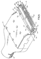
- FIGs 5 and 6 show the bottom of board-mounted connector 10 and a second pair of ground arms, generally designated 56, having contact portions 50 for engaging front face 16 of shield 14 of plug connector 12.
- Ground arms 56 are effective in connectors where it is found undesirable or impossible to provide a sufficiently long ground arm out of a single wall or side of the connector. In other words, it can be seen most clearly in Figure 6 that each ground arm 56 has a right-angular configuration.
- Each arm 56 has a first portion 58 contiguous with one of the end walls 38 of shield 30.
- Each arm is bent to form a second portion 60 which extends at a right angle to portion 58 and across the bottom side of the housing 20.
- board-mounted connector 10 does not have a bottom wall, effective shielding is achieved by using two ground arms 56.
- the two ground arms 56 represent multiple contacts which provide a lower impedance between the printed circuit board and the cable attached to the plug connector 12, a more balanced current flow through the shield and a balanced mechanical force completely around the contact edge of the shield.
- the ground arms 56 are combined with the copper grounding plate at the bottom of the printed circuit board, adequate electromechanical leakage is substantially reduced.
- the advantages of providing right-angled ground arms 56 are not limited to board-mounted connectors.
- the right-angled ground arms could be placed at the top wall of the shield, or on a plug shield at the intersection of any transverse walls of any shield or on a plug shield.
- the advantages are provided by forming a single ground arm out of two adjacent walls of a given shield, so that the ground arm can be lengthened beyond that which a single wall may possibly afford.
- the twisting action of portion 60 of ground arm 56 relative to portion 58 enhances the resiliency of the ground arm.
Landscapes
- Details Of Connecting Devices For Male And Female Coupling (AREA)
Abstract
An electromagnetic shield (30) is provided for at least one electronic
component (10). The shield includes an electrically conductive enclosure having
walls (36,38,40, 60) defining an open end (32) at a mating face (22) of the component.
A flexible elongated ground arm (42,44) is integrally formed from the walls and
extends generally parallel to the mating face (22). The ground arm includes a contact
portion (50) for engaging a conductive ground portion (14) of a complementary
mating electronic component (12). A portion (40) of the walls is folded over in an
area in registry with the ground arm (42,44) to minimize electromagnetic leakage
about the ground arm.
Description
This invention generally relates to the art of electrical connectors and,
particularly, to a shielded electrical connector having a new and improved electromagnetic
shield.
A wide variety of electrical connectors require protection against the
egress or ingress of radio frequency interference (RFI) and/or electromagnetic
interference (EMI). This is particularly true in electrical connectors used with high
speed electronic equipment. "EMI" has become fairly generic to describe most types
of interference caused by electronic waves.
EMI protection typically is provided by substantially enclosing a
connector, at least about its mating interface, with an electrically conductive shield.
Such shielding enclosures typically are stamped and formed from sheet metal material.
The shields are grounded, such as to a ground wire of an electrical cable or to a ground
circuit trace on a printed circuit board. When two connectors are mated, it is desirable
to have the shields of the two connectors in positive engagement to establish a
common ground therethrough and to prevent electromagnetic radiation from or to the
connectors in the area of the mating interface thereof.
Heretofore, EMI protection at the interface of a pair of mating
connectors has been accomplished simply by overlapping the two shields of the
respective connectors. Although this method is quite effective, it requires additional
space in the mating direction of the connectors and this is highly undesirable when
space is critical in miniaturized, high speed electronics. The same type of space
problem arises when radially extending flaps are used between the shields to establish
positive engagement, with the space problem being in the transverse direction rather
than the mating direction.
In order to solve the space problems described above, positive
engagement between a pair of shields of a pair of mating connectors has been
accomplished by using flexible, cantilevered ground arms which are stamped directly
out of a side wall of at least one of the shields at the mating interface of the
connectors. Although such flexible ground arms do not require additional space, they
create further problems in creating stamped openings about the arms through which
electromagnetic interference can pass. In addition, if the flexible arms are too short,
they are susceptible to failure due to stress and strain from numerous mating and
unmating cycles of the connectors. In other words, it is desirable to have relatively
long cantilevered ground arms, but the size of connectors often do not allow sufficient
dimensions to lengthen the arms. The present invention is directed to solving one or
more of this myriad of problems in shielded electrical connectors.
An object, therefore, of the invention is to provide a new and improved
electromagnetic shield for at least one electronic component.
Another object of the invention is to provide an electrical connector
with a new and improved electrically conductive shield.
In the exemplary embodiment of the invention, the electromagnetic
shield includes an electrically conductive enclosure having wall means defining an
open end at a mating face of the component. A flexible elongated ground arm is
integrally formed from the wall means and extends generally parallel to the mating
face. The ground arm includes a contact portion for engaging a conductive ground
portion of a complementary mating electronic component. A portion of the ground
means is folded over in an area in registry with said ground arm to minimize
electromagnetic leakage about the ground arm.
As disclosed herein, the enclosure is stamped and formed of conductive
sheet metal material. The ground arm is stamped from the wall means leaving an
opening about the ground arm. The folded over portion of the wall means is in
registry with at least a portion of the opening. The ground arm is cantilevered and
extends across a substantial portion of the mating face. The contact portion is at a
distal end of the cantilevered ground arm.
Other objects, features and advantages of the invention will be apparent
from the following detailed description taken in connection with the accompanying
drawings.
The features of this invention which are believed to be novel are set
forth with particularity in the appended claims. The invention, together with its
objects and the advantages thereof, may be best understood by reference to the
following description taken in conjunction with the accompanying drawings, in which
like reference numerals identify like elements in the figures and in which:
Referring to the drawings in greater detail, and first to Figure 1, the
invention is embodied in an electrical connector, generally designated 10, which is
adapted for mounting on a surface of a printed circuit board and which mates with a
plug connector, generally designated 12, which is adapted for terminating an electrical
cable. In other words, board-mounted connector 10 is a receptacle connector for
receiving plug connector 12.
Referring to Figure 2 in conjunction with Figure 1, board-mounted
connector 10 includes a dielectric housing, generally designated 20, which defines a
mating face 22 of the connector. The housing may be a one-piece structure unitarily
molded of dielectric material such as plastic or the like. The housing has a plurality
of through passages 24 which mount a plurality of terminals 26 which have solder tails
28 projecting from a rear of the housing for a solder connection to appropriate signal
and power circuit traces on the printed circuit board.
The invention is incorporated in an electrically conductive shield,
generally designated 30, which forms an electrically conductive enclosure substantially
about housing 20, leaving an open end 32 at mating face 20 of the connector.
The shield is stamped and formed of conductive sheet metal material and includes a
plurality of tail portions 34 for solder connection to appropriate ground traces on the
printed circuit board.
As seen best in Figure 2, stamped and formed sheet metal shield 30
includes wall means defined by a top wall 36 which forms the major top side of the
shield. The top wall is joined perpendicularly to a pair of end walls 38 which form
minor ends of the shield. A flap 40 is folded over the top of top wall 36. A flexible
elongated ground arm 42 is stamped out of top wall 36 so the ground arm is integral
with and cantilevered from the top wall. A second flexible elongated ground arm 44
is stamped out of flap 40 to be integral therewith and cantilevered therefrom. When
the ground arms are stamped, an opening 46 is formed behind ground arm 42, and an
opening 48 is formed behind ground arm 44. By criss-crossing the arms as seen in
Figure 2, each arm closes a good portion of the opening behind the other arm to
minimize the escape of electromagnetic interference therethrough and provides an
additional pathway for high frequency currents through capacitative coupling. Each
flexible ground arm 42 and 44 has a rounded contact portion 50 at the distal end
thereof for resiliently engaging front face 16 of shield 14 of plug connector 12 as seen
clearly in Figure 1. Therefore, upon mating of connectors 10 and 12, flexible
cantilevered ground arms 42 and 44 become spring loaded to establish good grounding
connections between shields 30 and 14 of connectors 10 and 12, respectively.
It should be understood that the use of two overlapping ground arms
42 and 44 is a preferred embodiment of the invention. However, by folding flap 40
over top wall 36, only one ground arm could be stamped out of either the flap or the
top wall, with the other of the flap or top wall completely blocking any opening
formed behind the single ground arm and through which electromagnetic interference
could pass.
Figures 3 and 4 simply show a portion of the stamping and forming
process for ground arms 42 and 44 and folding flap 40 over top wall 36 of shield 30.
In particularly, Figure 3 shows ground arm 42 having been stamped out of top wall 36
leaving opening 46 therebehind. Ground arm 44 is seen stamped out of what will
become flap 40, leaving opening 48 therebehind. Figure 4 shows flap 40 being folded
at 52 in the direction of arrow "A" whereupon the flap eventually will be folded onto
top wall 36 as seen in Figure 2. Of course, if only one ground arm 42 or 44 is stamped
out of top wall 36 or flap 40, the other of the top wall or flap will substantially entirely
close the opening about the single ground arm to completely eliminate or at least
minimize electromagnetic leakage about the ground arm.
Figures 5 and 6 show the bottom of board-mounted connector 10 and
a second pair of ground arms, generally designated 56, having contact portions 50 for
engaging front face 16 of shield 14 of plug connector 12. Ground arms 56 are
effective in connectors where it is found undesirable or impossible to provide a
sufficiently long ground arm out of a single wall or side of the connector. In other
words, it can be seen most clearly in Figure 6 that each ground arm 56 has a right-angular
configuration. Each arm 56 has a first portion 58 contiguous with one of the
end walls 38 of shield 30. Each arm is bent to form a second portion 60 which
extends at a right angle to portion 58 and across the bottom side of the housing 20.
Although board-mounted connector 10 does not have a bottom wall, effective
shielding is achieved by using two ground arms 56. The two ground arms 56
represent multiple contacts which provide a lower impedance between the printed
circuit board and the cable attached to the plug connector 12, a more balanced current
flow through the shield and a balanced mechanical force completely around the
contact edge of the shield. When the ground arms 56 are combined with the copper
grounding plate at the bottom of the printed circuit board, adequate electromechanical
leakage is substantially reduced.
The advantages of providing right-angled ground arms 56 are not
limited to board-mounted connectors. The right-angled ground arms could be placed
at the top wall of the shield, or on a plug shield at the intersection of any transverse
walls of any shield or on a plug shield. The advantages are provided by forming a
single ground arm out of two adjacent walls of a given shield, so that the ground arm
can be lengthened beyond that which a single wall may possibly afford. In addition,
the twisting action of portion 60 of ground arm 56 relative to portion 58 enhances the
resiliency of the ground arm.
It will be understood that the invention may be embodied in other
specific forms without departing from the spirit or central characteristics thereof. The
present examples and embodiments, therefore, are to be considered in all respects as
illustrative and not restrictive, and the invention is not to be limited to the details
given herein.
Claims (16)
- An electromagnetic shield (30) for at least one electronic component (10), comprising:an electrically conductive enclosure having wall means (36,38,40, 60) defining an open end (32) at a mating face (22) of the component;a flexible elongated ground arm (42,44) integrally formed from said wall means (36,40) and extending generally parallel to said mating face (22), the ground arm including a contact portion (50) for engaging a conductive ground portion (14) of a complementary mating electronic component (12); anda portion (40) of said wall means being folded over in an area in registry with said ground arm (42,44) to minimize electromagnetic leakage about the ground arm.
- The electromagnetic shield of claim 1 wherein said shield (30) is stamped and formed of conductive sheet metal material.
- The electromagnetic shield of claim 2 wherein said ground arm (42,44) is stamped from said wall means leaving an opening (46,48) about the ground arm, and said folded over portion (40) of the wall means being in registry with at least a portion of said opening.
- The electromagnetic shield of claim 1 wherein said ground arm (42,44) is cantilevered and extends across a substantial portion of said mating face (22).
- The electromagnetic shield of claim 4 wherein said contact portion (50) is at a distal end of the ground arm (42,44).
- The electromagnetic shield of claim 1, including one of said ground arms (42) in said wall means underlying said folded over portion (40) and a second of said ground arms (44) formed from the folded over portion.
- The electromagnetic shield of claim 6 wherein said two ground arms (42,44) criss-cross each other.
- An electromagnetic shield (30) for at least one electronic component (10), comprising:an electrically conductive enclosure stamped and formed of sheet metal material and having wall means (36,38,40, 60) defining an open end (32) at a mating face (22) of the component;a flexible elongated ground arm (42,44) stamped from said wall means leaving an opening (46,48) about the ground arm, the ground arm extending generally parallel to and across a substantial portion of said mating face (22), and the ground arm including a contact portion (50) for engaging a conductive ground portion (14) of a complementary mating electronic component (12); anda portion (40) of said wall means being folded over in registry with at least a portion of said opening (46,48) to minimize electromagnetic leakage about the ground arm (42,44).
- The electromagnetic shield of claim 8 wherein said contact portion (50) is at a distal end of the ground arm (42,44).
- An electrical connector (10), comprising:a dielectric housing (20) defining a mating face (22) of the connector;a plurality of terminals (26) mounted on the housing;an electrically conductive shield (30) about at least a portion of the dielectric housing (20) and having wall means (36,38,40, 60) defining an open end (32) about said mating face (22);a flexible elongated ground arm (42,44) integrally formed from said wall means (36,40) and extending generally parallel to said mating face (22), the ground arm including a contact portion (50) for engaging a conductive ground portion (14) of a complementary mating connector (12); anda portion (40) of said wall means being folded over in an area in registry with said ground arm (42,44) to minimize electromagnetic leakage about the ground arm.
- The electrical connector of claim 10 wherein said shield (30) is stamped and formed of conductive sheet metal material.
- The electrical connector of claim 11 wherein said ground arm (42,44) is stamped from said wall means leaving an opening (46,48) about the ground arm, and said folded over portion (40) of the wall means being in registry with at least a portion of said opening.
- The electrical connector of claim 10 wherein said ground arm (42,44) is cantilevered and extends across a substantial portion of said mating face (22).
- The electrical connector of claim 13 wherein said contact portion (50) is at a distal end of the ground arm (42,44).
- The electromagnetic shield of claim 10, including one of said ground arms (42) in said wall means underlying said folded over portion (40) and a second of said ground arms (44) formed from the folded over portion.
- The electromagnetic shield of claim 15 wherein said two ground arms (42,44) criss-cross each other.
Applications Claiming Priority (2)
| Application Number | Priority Date | Filing Date | Title |
|---|---|---|---|
| US409636 | 1999-10-01 | ||
| US09/409,636 US6200165B1 (en) | 1999-10-01 | 1999-10-01 | Shielded electrical connector with a folded wall |
Publications (1)
| Publication Number | Publication Date |
|---|---|
| EP1089395A1 true EP1089395A1 (en) | 2001-04-04 |
Family
ID=23621352
Family Applications (1)
| Application Number | Title | Priority Date | Filing Date |
|---|---|---|---|
| EP00120630A Withdrawn EP1089395A1 (en) | 1999-10-01 | 2000-09-21 | Shielded electrical connector with a folded wall |
Country Status (4)
| Country | Link |
|---|---|
| US (1) | US6200165B1 (en) |
| EP (1) | EP1089395A1 (en) |
| CN (1) | CN1183634C (en) |
| TW (1) | TW504053U (en) |
Cited By (1)
| Publication number | Priority date | Publication date | Assignee | Title |
|---|---|---|---|---|
| CN104978788A (en) * | 2015-06-17 | 2015-10-14 | 深圳粤宝电子工业总公司 | Currency detector magnetic head shielding cover manufacturing method and magnetic head shielding cover |
Families Citing this family (3)
| Publication number | Priority date | Publication date | Assignee | Title |
|---|---|---|---|---|
| US6807068B1 (en) * | 2001-06-04 | 2004-10-19 | Corvis Corporation | Optical and electrical systems and apparatuses including line interface assemblies and methods of operation |
| US9385481B2 (en) * | 2014-09-17 | 2016-07-05 | Kuang Ying Computer Equipment Co., Ltd. | Electronic connector |
| CN104868282B (en) * | 2015-05-07 | 2024-09-03 | 连展科技(深圳)有限公司 | Socket electric connector |
Citations (3)
| Publication number | Priority date | Publication date | Assignee | Title |
|---|---|---|---|---|
| US5637015A (en) * | 1995-08-31 | 1997-06-10 | Hon Hai Precision Ind. Co., Ltd. | Shielded electrical connector |
| US5800204A (en) * | 1995-11-09 | 1998-09-01 | Molex Incorporated | Electrical connector for flat cable |
| EP0893854A2 (en) * | 1997-07-23 | 1999-01-27 | Molex Incorporated | Shielded electrical connector |
Family Cites Families (12)
| Publication number | Priority date | Publication date | Assignee | Title |
|---|---|---|---|---|
| US4653836A (en) | 1983-07-06 | 1987-03-31 | Amp Incorporated | Shielded electrical connector |
| US4688868A (en) | 1986-05-14 | 1987-08-25 | Honeywell Information Systems Inc. | Grounding gasket for D-shell connector |
| US5178562A (en) | 1991-10-17 | 1993-01-12 | Epson Portland, Inc. | Contact member for miniature electrical circuit connector |
| US5295867A (en) | 1992-12-23 | 1994-03-22 | Itt Corporation | Edge connector shield |
| GB9307127D0 (en) | 1993-04-06 | 1993-05-26 | Amp Holland | Prestressed shielding plates for electrical connectors |
| JPH0818265A (en) | 1994-06-29 | 1996-01-19 | Molex Inc | Method of shielding electromagnetic wave, etc. on printed circuit board and shield cover therefor |
| US5622523A (en) | 1995-10-31 | 1997-04-22 | Hon Hai Precision Ind, Co., Ltd. | Grounding device for use with shielded DIN connector |
| US5738544A (en) * | 1996-06-27 | 1998-04-14 | The Whitaker Corporation | Shielded electrical connector |
| US5755595A (en) | 1996-06-27 | 1998-05-26 | Whitaker Corporation | Shielded electrical connector |
| US5702271A (en) * | 1996-08-30 | 1997-12-30 | The Whitaker Corporation | Ultra low profile board-mounted modular jack |
| US5913698A (en) * | 1997-05-01 | 1999-06-22 | Hon Hai Precision Ind. Co., Ltd. | Shielded connector |
| US6036544A (en) * | 1998-01-16 | 2000-03-14 | Molex Incorporated | Coupled electrical connector assembly |
-
1999
- 1999-10-01 US US09/409,636 patent/US6200165B1/en not_active Expired - Fee Related
-
2000
- 2000-09-21 EP EP00120630A patent/EP1089395A1/en not_active Withdrawn
- 2000-09-27 TW TW089216755U patent/TW504053U/en not_active IP Right Cessation
- 2000-09-30 CN CNB001323318A patent/CN1183634C/en not_active Expired - Fee Related
Patent Citations (3)
| Publication number | Priority date | Publication date | Assignee | Title |
|---|---|---|---|---|
| US5637015A (en) * | 1995-08-31 | 1997-06-10 | Hon Hai Precision Ind. Co., Ltd. | Shielded electrical connector |
| US5800204A (en) * | 1995-11-09 | 1998-09-01 | Molex Incorporated | Electrical connector for flat cable |
| EP0893854A2 (en) * | 1997-07-23 | 1999-01-27 | Molex Incorporated | Shielded electrical connector |
Cited By (1)
| Publication number | Priority date | Publication date | Assignee | Title |
|---|---|---|---|---|
| CN104978788A (en) * | 2015-06-17 | 2015-10-14 | 深圳粤宝电子工业总公司 | Currency detector magnetic head shielding cover manufacturing method and magnetic head shielding cover |
Also Published As
| Publication number | Publication date |
|---|---|
| CN1183634C (en) | 2005-01-05 |
| TW504053U (en) | 2002-09-21 |
| US6200165B1 (en) | 2001-03-13 |
| CN1290979A (en) | 2001-04-11 |
Similar Documents
| Publication | Publication Date | Title |
|---|---|---|
| US6595801B1 (en) | Electrical connector with electrically isolated ESD and EMI shields | |
| US5378172A (en) | Low profile shielded jack | |
| US5766041A (en) | Shield member for panel mount connector | |
| EP0188876B1 (en) | Shielded electrical connector assembly | |
| US5934940A (en) | Shielded electrical connector | |
| US5281169A (en) | Shielded electrical connector assemblies | |
| US6206728B1 (en) | Shielded electrical connector system | |
| EP0582726A1 (en) | Modular jack | |
| US20040259421A1 (en) | Cable connector assembly having improved shield members | |
| US6193555B1 (en) | ESD and crosstalk protected hybrid connector | |
| JPH10506222A (en) | Improved ground shroud for electrical connectors | |
| JPH02195675A (en) | Low profile shield jack | |
| US6361332B1 (en) | Retention system for electrical connectors | |
| US6739915B1 (en) | Electrical connector with rear retention mechanism of outer shell | |
| US6264504B1 (en) | Electrical connector | |
| EP1480294B1 (en) | Connector enhanced in electromagnetic shielding function | |
| US6210228B1 (en) | Shielded electrical connector | |
| EP1126552A2 (en) | Circuit board straddle mounted connector | |
| US6416358B1 (en) | Shielded electrical connector for mounting on a printed circuit board | |
| US6200165B1 (en) | Shielded electrical connector with a folded wall | |
| US20030119354A1 (en) | Electrical connector having improved shielding | |
| US6106334A (en) | Shielded cable connector | |
| JP3409208B2 (en) | Shielded electrical connector with folding wall | |
| CN2458775Y (en) | Electric connector | |
| EP1045484A1 (en) | Shielded electrical connector |
Legal Events
| Date | Code | Title | Description |
|---|---|---|---|
| PUAI | Public reference made under article 153(3) epc to a published international application that has entered the european phase |
Free format text: ORIGINAL CODE: 0009012 |
|
| AK | Designated contracting states |
Kind code of ref document: A1 Designated state(s): DE FR GB IT |
|
| AX | Request for extension of the european patent |
Free format text: AL;LT;LV;MK;RO;SI |
|
| 17P | Request for examination filed |
Effective date: 20010924 |
|
| AKX | Designation fees paid |
Free format text: DE FR GB IT |
|
| STAA | Information on the status of an ep patent application or granted ep patent |
Free format text: STATUS: THE APPLICATION HAS BEEN WITHDRAWN |
|
| 18W | Application withdrawn |
Withdrawal date: 20020822 |