EP1087477A2 - Semiconductor laser module - Google Patents
Semiconductor laser module Download PDFInfo
- Publication number
- EP1087477A2 EP1087477A2 EP00120186A EP00120186A EP1087477A2 EP 1087477 A2 EP1087477 A2 EP 1087477A2 EP 00120186 A EP00120186 A EP 00120186A EP 00120186 A EP00120186 A EP 00120186A EP 1087477 A2 EP1087477 A2 EP 1087477A2
- Authority
- EP
- European Patent Office
- Prior art keywords
- semiconductor laser
- feedback portion
- light feedback
- light
- laser module
- Prior art date
- Legal status (The legal status is an assumption and is not a legal conclusion. Google has not performed a legal analysis and makes no representation as to the accuracy of the status listed.)
- Granted
Links
Images







Classifications
-
- H—ELECTRICITY
- H01—ELECTRIC ELEMENTS
- H01S—DEVICES USING THE PROCESS OF LIGHT AMPLIFICATION BY STIMULATED EMISSION OF RADIATION [LASER] TO AMPLIFY OR GENERATE LIGHT; DEVICES USING STIMULATED EMISSION OF ELECTROMAGNETIC RADIATION IN WAVE RANGES OTHER THAN OPTICAL
- H01S5/00—Semiconductor lasers
- H01S5/10—Construction or shape of the optical resonator, e.g. extended or external cavity, coupled cavities, bent-guide, varying width, thickness or composition of the active region
- H01S5/14—External cavity lasers
- H01S5/146—External cavity lasers using a fiber as external cavity
-
- H—ELECTRICITY
- H01—ELECTRIC ELEMENTS
- H01S—DEVICES USING THE PROCESS OF LIGHT AMPLIFICATION BY STIMULATED EMISSION OF RADIATION [LASER] TO AMPLIFY OR GENERATE LIGHT; DEVICES USING STIMULATED EMISSION OF ELECTROMAGNETIC RADIATION IN WAVE RANGES OTHER THAN OPTICAL
- H01S3/00—Lasers, i.e. devices using stimulated emission of electromagnetic radiation in the infrared, visible or ultraviolet wave range
- H01S3/05—Construction or shape of optical resonators; Accommodation of active medium therein; Shape of active medium
- H01S3/08—Construction or shape of optical resonators or components thereof
- H01S3/081—Construction or shape of optical resonators or components thereof comprising three or more reflectors
- H01S3/082—Construction or shape of optical resonators or components thereof comprising three or more reflectors defining a plurality of resonators, e.g. for mode selection or suppression
- H01S3/0823—Construction or shape of optical resonators or components thereof comprising three or more reflectors defining a plurality of resonators, e.g. for mode selection or suppression incorporating a dispersive element, e.g. a prism for wavelength selection
- H01S3/0826—Construction or shape of optical resonators or components thereof comprising three or more reflectors defining a plurality of resonators, e.g. for mode selection or suppression incorporating a dispersive element, e.g. a prism for wavelength selection using a diffraction grating
-
- H—ELECTRICITY
- H01—ELECTRIC ELEMENTS
- H01S—DEVICES USING THE PROCESS OF LIGHT AMPLIFICATION BY STIMULATED EMISSION OF RADIATION [LASER] TO AMPLIFY OR GENERATE LIGHT; DEVICES USING STIMULATED EMISSION OF ELECTROMAGNETIC RADIATION IN WAVE RANGES OTHER THAN OPTICAL
- H01S5/00—Semiconductor lasers
- H01S5/02—Structural details or components not essential to laser action
- H01S5/022—Mountings; Housings
- H01S5/02208—Mountings; Housings characterised by the shape of the housings
- H01S5/02216—Butterfly-type, i.e. with electrode pins extending horizontally from the housings
-
- H—ELECTRICITY
- H01—ELECTRIC ELEMENTS
- H01S—DEVICES USING THE PROCESS OF LIGHT AMPLIFICATION BY STIMULATED EMISSION OF RADIATION [LASER] TO AMPLIFY OR GENERATE LIGHT; DEVICES USING STIMULATED EMISSION OF ELECTROMAGNETIC RADIATION IN WAVE RANGES OTHER THAN OPTICAL
- H01S5/00—Semiconductor lasers
- H01S5/02—Structural details or components not essential to laser action
- H01S5/022—Mountings; Housings
- H01S5/0225—Out-coupling of light
- H01S5/02251—Out-coupling of light using optical fibres
-
- H—ELECTRICITY
- H01—ELECTRIC ELEMENTS
- H01S—DEVICES USING THE PROCESS OF LIGHT AMPLIFICATION BY STIMULATED EMISSION OF RADIATION [LASER] TO AMPLIFY OR GENERATE LIGHT; DEVICES USING STIMULATED EMISSION OF ELECTROMAGNETIC RADIATION IN WAVE RANGES OTHER THAN OPTICAL
- H01S5/00—Semiconductor lasers
- H01S5/10—Construction or shape of the optical resonator, e.g. extended or external cavity, coupled cavities, bent-guide, varying width, thickness or composition of the active region
- H01S5/12—Construction or shape of the optical resonator, e.g. extended or external cavity, coupled cavities, bent-guide, varying width, thickness or composition of the active region the resonator having a periodic structure, e.g. in distributed feedback [DFB] lasers
- H01S5/1206—Construction or shape of the optical resonator, e.g. extended or external cavity, coupled cavities, bent-guide, varying width, thickness or composition of the active region the resonator having a periodic structure, e.g. in distributed feedback [DFB] lasers having a non constant or multiplicity of periods
- H01S5/1215—Multiplicity of periods
Definitions
- the polarization fluctuation preventing means is a birefringent fiber.
- the semiconductor laser has an oscillating wavelength in a band centered at 980 nm.
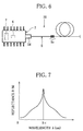
- the package 2 accommodates the Peltier element 3, the base 4, one end side of the optical fiber 5, the semiconductor laser 6, the photodiode 7, and so on.
- the package 2 has a bottom plate 2a, a peripheral wall 2b, and a cover 2c, and the cover 2c is attached on the peripheral wall 2b.
- the package 2 is also provided with a sleeve 2d extending from the peripheral wall 2b.
- a second ferrule 5b, later described, of the optical fiber 5 is inserted into the sleeve 2d.
- the package 2 is filled with a nitrogen gas, for example, to have an inert gas atmosphere in the interior.
- the base 4 carries the semiconductor laser 6 through a first carrier 8 and a heat sink 9. Also, disposed on the base 4 are a second carrier 10 near a rear end facet 6b of the semiconductor laser 6, and a first ferrule 5a attached to one end of the optical fiber 5 near a front end facet 6a of the semiconductor laser 6.
- the chirped grating may be formed to have a reflection wavelength characteristic by combining arbitrary light feedback portions with one another.
- the semiconductor laser 6 and the FBG may be selected such that the wavelength dependence on the right side of equation (2) determined by the FGB1 to FBGn has an intersection with the wavelength dependence of the left side of equation (2) determined by the characteristic of the semiconductor laser 6 only at the first light feedback portion (FBG1).
Landscapes
- Physics & Mathematics (AREA)
- Condensed Matter Physics & Semiconductors (AREA)
- General Physics & Mathematics (AREA)
- Electromagnetism (AREA)
- Optics & Photonics (AREA)
- Optical Couplings Of Light Guides (AREA)
- Semiconductor Lasers (AREA)
Abstract
Description
Claims (17)
- A semiconductor laser module comprising:a semiconductor laser having a front end facet from which output light is emitted;an optical fiber on which the output light emitted from said semiconductor laser is incident, said optical fiber having a light feedback portion for reflecting light at a predetermined wavelength; anda package for accommodating said semiconductor laser together with one end side of said optical fiber,
wherein said light feedback portion includes a first light feedback portion set at a predetermined reflection center wavelength for determining an oscillating wavelength of said semiconductor laser, and at least one second light feedback portion. - The semiconductor laser module according to claim 1, wherein said second light feedback portion has a reflectance equal to or lower than a maximum reflectance of the first light feedback portion at least within a wavelength range of a full width half maximum in the first light feedback portion.
- The semiconductor laser module according to claim 1 or 2, wherein said second light feedback portion has a reflection center wavelength substantially identical to that of said first light feedback portion.
- The semiconductor laser module according to claim 3, wherein a difference in the reflection center wavelength between said first light feedback portion and said second light feedback portion is set within 2 nm.
- The semiconductor laser module according to claim 1 or 2, wherein said first light feedback portion differs from said second light feedback portion in the reflection center wavelength.
- The semiconductor laser module according to claim 1, wherein said second light feedback portion has a flat reflection level characteristic substantially without wavelength dependence, and a reflectance lower than a maximum reflectance of said first light feedback portion.
- The semiconductor laser module according to any one of claims 1 to 6, wherein either said first or said second light feedback portion comprises a fiber bragg grating.
- The semiconductor laser module according to any one of claims 1 to 7, wherein said first light feedback portion and an adjacent one of said second light feedback portions are spaced by a distance set equal to or longer than 5 mm between longitudinal center positions thereof.
- The semiconductor laser module according to any one of claims 1 to 8, wherein two or more of light feedback portions chosen from the first light feedback portion and the at least one second light feedback portion comprise a chirped bragg grating having a reflection characteristic which is superposition of respective reflection characteristics.
- The semiconductor laser module according to any one of claims 1 to 9, wherein said light feedback portion is positioned external to said package.
- The semiconductor laser module according to any one of claims 1 to 10, wherein said optical fiber includes polarization fluctuation preventing means disposed between said semiconductor laser and said light feedback portion for preventing fluctuations in light polarization.
- The semiconductor laser module according to claim 11, wherein said polarization fluctuation preventing means is a birefringent fiber.
- The semiconductor laser module according to claim 12, wherein said birefringent fiber is any of a PANDA fiber which has a core applied with a non-axially symmetric stress and a stress applying portion of circular cross-section; a bow-tie fiber of a fan-shaped cross-section; an elliptic jacket fiber of elliptic cross-section; and an elliptic core fiber having a core waveguide structure in a non-axially symmetric form and a core of elliptic cross-section.
- The semiconductor laser module according to any one of claims 1 to 13, wherein a distance from a rear end facet of said semiconductor laser to a longitudinal center position of either said first or said second light feedback portion is 10 cm or longer.
- The semiconductor laser module according to any one of claims 1 to 14, wherein said semiconductor laser has an oscillating wavelength in 980 nm band.
- The semiconductor laser module according to any one of claims 1 to 15, wherein said optical fiber is a lensed fiber, wherein light emitted from said semiconductor laser is coupled to a distal end of said lensed fiber.
- The semiconductor laser module according to claim 16, wherein said lensed fiber is made by connecting by fusion said optical fiber formed with said first light feedback portion and/or said second light feedback portion.
Applications Claiming Priority (2)
| Application Number | Priority Date | Filing Date | Title |
|---|---|---|---|
| JP27093799 | 1999-09-24 | ||
| JP27093799 | 1999-09-24 |
Publications (3)
| Publication Number | Publication Date |
|---|---|
| EP1087477A2 true EP1087477A2 (en) | 2001-03-28 |
| EP1087477A3 EP1087477A3 (en) | 2002-07-24 |
| EP1087477B1 EP1087477B1 (en) | 2006-08-23 |
Family
ID=17493089
Family Applications (1)
| Application Number | Title | Priority Date | Filing Date |
|---|---|---|---|
| EP00120186A Expired - Lifetime EP1087477B1 (en) | 1999-09-24 | 2000-09-22 | Semiconductor laser module |
Country Status (2)
| Country | Link |
|---|---|
| US (1) | US6524016B1 (en) |
| EP (1) | EP1087477B1 (en) |
Cited By (1)
| Publication number | Priority date | Publication date | Assignee | Title |
|---|---|---|---|---|
| WO2003005500A3 (en) * | 2001-07-06 | 2004-01-15 | Intel Corp | Hermetically sealed external cavity laser system and method |
Families Citing this family (9)
| Publication number | Priority date | Publication date | Assignee | Title |
|---|---|---|---|---|
| US6839517B2 (en) * | 2001-02-12 | 2005-01-04 | Agere Systems Inc. | Apparatus and method for transmitting optical signals through a single fiber optical network |
| US6860651B2 (en) * | 2001-06-26 | 2005-03-01 | Derosa Michael E. | Method and device for removing heat from a fiber-optic package |
| JP2004177905A (en) * | 2001-12-25 | 2004-06-24 | Mitsubishi Electric Corp | Optical module |
| JP3909257B2 (en) * | 2002-03-12 | 2007-04-25 | 日本オプネクスト株式会社 | Optical coupling device |
| US7120178B2 (en) * | 2002-06-15 | 2006-10-10 | Intel Corporation | Chip carrier apparatus and method |
| WO2005031930A1 (en) | 2003-09-26 | 2005-04-07 | The Furukawa Electric Co., Ltd. | Semiconductor laser |
| US7258495B1 (en) * | 2005-06-24 | 2007-08-21 | Corning Incorporated | Lensed fiber stub assemblies optical and optoelectronic packages including them |
| US10425156B1 (en) * | 2018-03-30 | 2019-09-24 | Facebook, Inc. | Dynamically determining optical transceiver expected life |
| US10461851B1 (en) | 2018-03-30 | 2019-10-29 | Facebook, Inc. | Predicting optical transceiver failure |
Family Cites Families (7)
| Publication number | Priority date | Publication date | Assignee | Title |
|---|---|---|---|---|
| US5305336A (en) | 1992-01-29 | 1994-04-19 | At&T Bell Laboratories | Compact optical pulse source |
| FR2720198B1 (en) * | 1994-05-20 | 1996-07-19 | France Telecom | Linearly polarized fiber optic laser. |
| US5659559A (en) * | 1994-06-28 | 1997-08-19 | Sdl, Inc. | Apparatus for generating a stabilized laser source |
| EP0798830B1 (en) | 1996-08-09 | 2000-10-25 | Dieter Huhse | Wavelength switchable gain-switched Fabry-Perot semiconductor laser |
| JP3206536B2 (en) * | 1997-02-21 | 2001-09-10 | 住友電気工業株式会社 | Semiconductor laser module |
| US6282340B1 (en) * | 1998-04-23 | 2001-08-28 | The Furukawa Electric Co., Ltd. | Light wavelength tuning device and light source optical demultiplexer and wavelength division multiplexed optical communication system using the tuning device |
| US6188712B1 (en) * | 1998-11-04 | 2001-02-13 | Optigain, Inc. | Asymmetrical distributed feedback fiber laser |
-
2000
- 2000-09-22 EP EP00120186A patent/EP1087477B1/en not_active Expired - Lifetime
- 2000-09-22 US US09/667,825 patent/US6524016B1/en not_active Expired - Lifetime
Cited By (3)
| Publication number | Priority date | Publication date | Assignee | Title |
|---|---|---|---|---|
| WO2003005500A3 (en) * | 2001-07-06 | 2004-01-15 | Intel Corp | Hermetically sealed external cavity laser system and method |
| US6788724B2 (en) | 2001-07-06 | 2004-09-07 | Intel Corporation | Hermetically sealed external cavity laser system and method |
| CN1319229C (en) * | 2001-07-06 | 2007-05-30 | 英特尔公司 | Hermetically sealed external cavity laser system and method |
Also Published As
| Publication number | Publication date |
|---|---|
| EP1087477B1 (en) | 2006-08-23 |
| EP1087477A3 (en) | 2002-07-24 |
| US6524016B1 (en) | 2003-02-25 |
Similar Documents
| Publication | Publication Date | Title |
|---|---|---|
| EP0860917B1 (en) | Semiconductor laser module | |
| US7599405B2 (en) | Method and apparatus for coherently combining multiple laser oscillators | |
| US5255274A (en) | Broadband laser source | |
| EP1107404B1 (en) | Fibre grating stabilized diode laser | |
| US6433920B1 (en) | Raman-based utility optical amplifier | |
| KR20010102076A (en) | Fiber grating-stabilized, semiconductor pump source | |
| US6947463B2 (en) | Semiconductor laser device for use in a laser module | |
| JPH11214799A (en) | Semiconductor laser module | |
| US6614823B2 (en) | Semiconductor laser device having a diffraction grating on a light reflection side | |
| EP1087477B1 (en) | Semiconductor laser module | |
| JP2002141607A (en) | Semiconductor laser module and optical amplifier using it | |
| JP4712178B2 (en) | Semiconductor laser module, laser unit, Raman amplifier, and method for suppressing Brillouin scattering and polarization degree of optical semiconductor laser module used in Raman amplifier | |
| EP0150214A1 (en) | LASER WITH COUPLED RESONATORS. | |
| US6934311B2 (en) | Semiconductor laser module and Raman amplifier | |
| EP1318583A2 (en) | Semiconductor laser with two active layers and optical fiber amplifier using the same | |
| US7099072B2 (en) | Direct optical modulation type wavelength converter | |
| JP2000151014A (en) | Optical function element and optical communication device | |
| US20040057485A1 (en) | Semiconductor laser device, semiconductor laser module, and optical fiber amplifier | |
| JP3833882B2 (en) | Semiconductor laser module | |
| JP2002374037A (en) | Semiconductor laser module, fiber amplifier and optical communication system using the same | |
| US20020176466A1 (en) | Semiconductor laser device, semiconductor laser module, and raman amplifier using the device or module | |
| JP2002118325A (en) | Semiconductor laser module and excitation light source device using the same | |
| JP4809554B2 (en) | Semiconductor laser module and Raman amplifier using the same | |
| US6944203B2 (en) | Multimode light generating module, semiconductor laser apparatus, and optical fiber amplifier | |
| EP1255335A2 (en) | Semiconductor laser device having a diffraction grating on a light reflection side |
Legal Events
| Date | Code | Title | Description |
|---|---|---|---|
| PUAI | Public reference made under article 153(3) epc to a published international application that has entered the european phase |
Free format text: ORIGINAL CODE: 0009012 |
|
| AK | Designated contracting states |
Kind code of ref document: A2 Designated state(s): AT BE CH CY DE DK ES FI FR GB GR IE IT LI LU MC NL PT SE |
|
| AX | Request for extension of the european patent |
Free format text: AL;LT;LV;MK;RO;SI |
|
| PUAL | Search report despatched |
Free format text: ORIGINAL CODE: 0009013 |
|
| AK | Designated contracting states |
Kind code of ref document: A3 Designated state(s): AT BE CH CY DE DK ES FI FR GB GR IE IT LI LU MC NL PT SE |
|
| AX | Request for extension of the european patent |
Free format text: AL;LT;LV;MK;RO;SI |
|
| RIC1 | Information provided on ipc code assigned before grant |
Free format text: 7H 01S 5/068 A, 7H 01S 5/14 B |
|
| 17P | Request for examination filed |
Effective date: 20021216 |
|
| AKX | Designation fees paid |
Designated state(s): FR GB |
|
| REG | Reference to a national code |
Ref country code: DE Ref legal event code: 8566 |
|
| 17Q | First examination report despatched |
Effective date: 20030926 |
|
| GRAP | Despatch of communication of intention to grant a patent |
Free format text: ORIGINAL CODE: EPIDOSNIGR1 |
|
| RIN1 | Information on inventor provided before grant (corrected) |
Inventor name: IRIE, YUICHIRO,THE FURUKAWA ELECTRIC CO., LTD. Inventor name: YAMAGUCHI, TAKEHARU,THE FURUKAWA ELECTRIC CO.,LTD Inventor name: OHKI, YUTAKA,THE FURUKAWA ELECTRIC CO., LTD. |
|
| GRAS | Grant fee paid |
Free format text: ORIGINAL CODE: EPIDOSNIGR3 |
|
| GRAA | (expected) grant |
Free format text: ORIGINAL CODE: 0009210 |
|
| AK | Designated contracting states |
Kind code of ref document: B1 Designated state(s): FR GB |
|
| REG | Reference to a national code |
Ref country code: GB Ref legal event code: FG4D |
|
| ET | Fr: translation filed | ||
| PLBE | No opposition filed within time limit |
Free format text: ORIGINAL CODE: 0009261 |
|
| STAA | Information on the status of an ep patent application or granted ep patent |
Free format text: STATUS: NO OPPOSITION FILED WITHIN TIME LIMIT |
|
| 26N | No opposition filed |
Effective date: 20070524 |
|
| REG | Reference to a national code |
Ref country code: FR Ref legal event code: PLFP Year of fee payment: 16 |
|
| REG | Reference to a national code |
Ref country code: FR Ref legal event code: PLFP Year of fee payment: 17 |
|
| REG | Reference to a national code |
Ref country code: FR Ref legal event code: PLFP Year of fee payment: 18 |
|
| REG | Reference to a national code |
Ref country code: FR Ref legal event code: PLFP Year of fee payment: 19 |
|
| PGFP | Annual fee paid to national office [announced via postgrant information from national office to epo] |
Ref country code: FR Payment date: 20190815 Year of fee payment: 20 |
|
| PGFP | Annual fee paid to national office [announced via postgrant information from national office to epo] |
Ref country code: GB Payment date: 20190920 Year of fee payment: 20 |
|
| REG | Reference to a national code |
Ref country code: GB Ref legal event code: PE20 Expiry date: 20200921 |
|
| PG25 | Lapsed in a contracting state [announced via postgrant information from national office to epo] |
Ref country code: GB Free format text: LAPSE BECAUSE OF EXPIRATION OF PROTECTION Effective date: 20200921 |