EP1087382A2 - Method of detecting a reproduction signal and circuit therefor - Google Patents
Method of detecting a reproduction signal and circuit therefor Download PDFInfo
- Publication number
- EP1087382A2 EP1087382A2 EP00308236A EP00308236A EP1087382A2 EP 1087382 A2 EP1087382 A2 EP 1087382A2 EP 00308236 A EP00308236 A EP 00308236A EP 00308236 A EP00308236 A EP 00308236A EP 1087382 A2 EP1087382 A2 EP 1087382A2
- Authority
- EP
- European Patent Office
- Prior art keywords
- signal
- signals
- optical
- outputs
- detection device
- Prior art date
- Legal status (The legal status is an assumption and is not a legal conclusion. Google has not performed a legal analysis and makes no representation as to the accuracy of the status listed.)
- Granted
Links
Images



Classifications
-
- G—PHYSICS
- G11—INFORMATION STORAGE
- G11B—INFORMATION STORAGE BASED ON RELATIVE MOVEMENT BETWEEN RECORD CARRIER AND TRANSDUCER
- G11B7/00—Recording or reproducing by optical means, e.g. recording using a thermal beam of optical radiation by modifying optical properties or the physical structure, reproducing using an optical beam at lower power by sensing optical properties; Record carriers therefor
-
- G—PHYSICS
- G11—INFORMATION STORAGE
- G11B—INFORMATION STORAGE BASED ON RELATIVE MOVEMENT BETWEEN RECORD CARRIER AND TRANSDUCER
- G11B7/00—Recording or reproducing by optical means, e.g. recording using a thermal beam of optical radiation by modifying optical properties or the physical structure, reproducing using an optical beam at lower power by sensing optical properties; Record carriers therefor
- G11B7/004—Recording, reproducing or erasing methods; Read, write or erase circuits therefor
- G11B7/005—Reproducing
-
- G—PHYSICS
- G11—INFORMATION STORAGE
- G11B—INFORMATION STORAGE BASED ON RELATIVE MOVEMENT BETWEEN RECORD CARRIER AND TRANSDUCER
- G11B20/00—Signal processing not specific to the method of recording or reproducing; Circuits therefor
- G11B20/10—Digital recording or reproducing
- G11B20/10009—Improvement or modification of read or write signals
-
- G—PHYSICS
- G11—INFORMATION STORAGE
- G11B—INFORMATION STORAGE BASED ON RELATIVE MOVEMENT BETWEEN RECORD CARRIER AND TRANSDUCER
- G11B20/00—Signal processing not specific to the method of recording or reproducing; Circuits therefor
- G11B20/22—Signal processing not specific to the method of recording or reproducing; Circuits therefor for reducing distortions
Definitions
- the present invention relates to detection of a reproduction signal, and more particularly, to a method of detecting only some of the outputs of an optical detection device, which are the least distorted or degraded, in an optical recording/reproduction system, and a circuit thereof.
- data is manifested on a disk in the form of pits on a substrate or modifications of a recording film.
- Data on a disk is detected by illuminating the disk with a laser, and detecting light reflected back.
- a signal is degraded due to a time delay between the outputs of an optical detection device caused by the geometry (for example, the width, the length, the depth and the angle) of a data pit and a recording domain, and due to a time delay caused by the interference between data in a tangential direction.
- a time delay is caused between the outputs of an optical detection device, a reproduction signal is distorted.
- the performance of the system is degraded.
- Optical discs are being developed for high-density recording and high-speed reproduction, to record and/or reproduce a high definition (HD) image.
- HD high definition
- a pickup unit (P/U) 102 radiates a beam emitted from a light source (for example, a laser diode) to the disc 100, and a multi-section optical detection device 104 (which can also be called a detection sensor), which is usually made up of a photodetector (PD), receives and divides an optical signal reflected by the disc 100 into multiple signals.
- a light source for example, a laser diode
- a multi-section optical detection device 104 which can also be called a detection sensor
- PD photodetector
- First, second, third and fourth current/voltage (I/V) converters 106, 108, 110 and 112 convert current signals A, B, C and D output by the optical detection device 104 into voltage signals.
- An arithmetic unit 114 sums the voltage signals output by the first, second, third and fourth I/V converters 106, 108, 110 and 112, and outputs the sum as a radio frequency reproducing signal RF SUM.
- a method of detecting a reproducing signal by simple addition of the outputs of the I/V converters 106, 108, 110 and 112 is adopted, so that a reproducing signal is degraded due to the data conditions recorded on a disc, crosstalk, the interference between optical signals reflected/diffracted from pits in close proximity and from adjacent tracks on a recording medium, and other problems with a system (for example, defocusing, detracking and tilting). Therefore, the quality of a reproducing signal and the performance of a system are degraded.
- An aim of the present invention is to provide a method of detecting an optimal reproducing signal while overcoming problems caused by data conditions, crosstalk, and the interference between optical signals reflected/diffracted from pits in close proximity and from adjacent tracks on a recording medium.
- Preferred embodiments of the invention aim to provide a method of detecting an optimal reproducing signal while overcoming defocusing and/or detracking and/or radial tilting and/or tangential tilting.
- Another aim of the present invention is to provide a method of detecting an optimal reproducing signal by adaptively compensating for signal interference caused by data conditions, crosstalk, the interference between optical signals reflected/diffracted from pits in close proximity and from adjacent tracks on a recording medium, defocusing, detracking, radial tilting and/or tangential tilting.
- a further aim of the present invention is to provide a circuit for detecting a reproducing signal, in which only some of the outputs of an optical detection device, that are the least degraded, are reproduced depending on data conditions, the interference between optical signals reflected/diffracted from pits in close proximity and from adjacent tracks on a recording medium, and/or the state of the system.
- a method of detecting a reproducing signal using an optical detection device for receiving an optical signal reflected from an optical recording medium and dividing the received signal into multiple signals corresponding to sections of the optical detection device which are arranged in a matrix with rows in the tangential direction and columns in the radial direction of the optical recording medium including the steps of: (a) selecting some signals, which are less degraded than other signals, from among the output signals of the optical detection device, on the basis of data conditions recorded on the optical recording medium, the interference between optical signals reflected/diffracted from pits in close proximity and from adjacent tracks on a recording medium, and/or various system states; and (b) obtaining a reproducing signal from the selected signals by compensating for the amount of signal interference caused due to data conditions, the interference between optical signals reflected/diffracted from pits in close proximity and from adjacent tracks on a recording medium, and/or various system states, on the basis of the results of the detection.
- a device for detecting a reproducing signal using an optical detection device including a photodetecting means for receiving an optical signal reflected from an optical recording medium and dividing the received signal into multiple signals, the device including a detector, a control unit and a compensator.
- the detector detects the outputs of the optical detection device corresponding to a combination of signals corresponding to sections of the photodetecting means arranged in the track direction, the outputs corresponding to a combination of signals corresponding to sections of the photodetecting means arranged in the radial direction, and/or the outputs corresponding to a combination of signals corresponding to sections of the photodetecting means arranged diagonally.
- the control unit provides a selection control signal and a compensation signal on the basis of the results of detection of data conditions recorded on the optical recording medium, the interference between optical signals reflected/diffracted from pits in close proximity and from adjacent tracks on a recording medium, and/or various system states.
- the compensator selects some of the outputs of the optical detection device provided via the detector in response to the selection control signal, and adaptively compensates for the selected outputs in response to the compensation signal.
- a pickup unit (P/U) 202 moves to a location from which information recorded on a disc 200 is detected, and projects a beam emitted from a light source (laser diode) to the disc 200.
- An n-section optical detection device 204 receives and divides an optical signal reflected back from the disc 200 into multiple signals.
- the optical detection device 204 groups multiple outputs into two parts by combining the multiple outputs in the radial direction, the track direction or diagonally depending on the data conditions, the interference between optical signals reflected/diffracted from pits in close proximity and from adjacent tracks on a recording medium, or the state of a system (for example, problems with focusing, tracking, or tilting).
- the multiple outputs of the optical detection device 204 are grouped into degraded output signals and less degraded output signals.
- a signal used as a reproducing signal is automatically selected by a system state detector 226 for detecting the state of a system (for example, focusing or defocusing, tracking or detracking, and tilting), the data conditions, or the interference between optical signals reflected/diffracted from pits in close proximity and from adjacent tracks on a recording medium.
- Some detection signals of the optical detection device 204 which are selected to compensate for abnormal operating conditions, detected data conditions, or detected interference between optical signals reflected/diffracted from pits in close proximity and from adjacent tracks on a recording medium, are adaptively equalized, so that an optimal reproducing signal is detected.
- first, second, third and fourth current/voltage (I/V) converters 206, 208, 210 and 212 convert current signals A, B, C and D output by the optical detection device 204 into voltage signals.
- a first adder 214 adds a voltage signal output from the first I/V converter 206, which corresponds to the output A of the optical detection device 204, to a voltage signal output from the second I/V converter 208, which corresponds to the output B of the optical detection device 204, and outputs the sum (A+B) as a signal R1.
- a second adder 216 adds a voltage signal output from the third I/V converter 210, which corresponds to the output C of the optical detection device 204, to a voltage signal output from the fourth I/V converter 212, which corresponds to the output D of the optical detection device 204, and outputs the sum (C+D) as a signal R2.
- the outputs A and B of the optical detection device 204 having the same distance from the center of the disk, and the outputs C and D of the optical detection device 204 having the same distance from the center of the disk.
- a third adder 218 adds a voltage signal output from the first I/V converter 206, which corresponds to the output A of the optical detection device 204, to a voltage signal output from the fourth I/V converter 212, which corresponds to the output D of the optical detection device 204, and outputs the sum (A+D) as a signal T1.
- a fourth adder 220 adds a voltage signal output from the second I/V converter 208, which corresponds to the output B of the optical detection device 204, to a voltage signal output from the third I/V converter 210, which corresponds to the output C of the optical detection device 204, and outputs the sum (B+C) as a signal T2.
- the outputs A and D of the optical detection device 204 are on the same level in a track direction, and the outputs B and C of the optical detection device 204 are on the same level in a track direction. Accordingly, a time delay is generated between the output of the optical detection device 204 supplied via the third adder 218 and the output of the optical detection device 204 supplied via the fourth adder 220, in a track direction, due to data conditions, crosstalk, or the interference between optical signals reflected/diffracted from pits in close proximity and from adjacent tracks on a recording medium.
- a fifth adder 222 adds a voltage signal output from the first I/V converter 206, which corresponds to the output A of the optical detection device 204, to a voltage signal output from the third I/V converter 210, which corresponds to the output C of the optical detection device 204, and outputs the sum (A+C) as a signal X1.
- a sixth adder 224 adds a voltage signal output from the second I/V converter 208, which corresponds to the output B of the optical detection device 204, to a voltage signal output from the fourth I/V converter 212, which corresponds to the output D of the optical detection device 204, and outputs the sum (B+D) as a signal X2.
- the outputs of the fifth and sixth adders 222 and 224 are used when defocusing occurs, since they are obtained by adding diagonally-aligned outputs among the outputs of the optical detection device 204.
- the system state detector 226 detects not only the system state (for example, defocusing, detracking and tilting) but also the data conditions and the interference between optical signals reflected/diffracted from pits in close proximity and from adjacent tracks on a recording medium, and provides a selection control signal to a selector 228 so that at least one good-performance signal is selected from among the outputs of the first through sixth adders 214 through 224 depending on a detected system state, detected data conditions and/or detected interference between optical signals reflected/diffracted from pits in close proximity and from adjacent tracks on a recording medium. Also, the system state detector 226 calculates an adaptive equalization amount for compensating for the detected system state, the detected data conditions and/or the detected interference between data, and provides the adaptive equalization amount to first through sixth equalizers 230 through 240.
- the system state detector 226 calculates an adaptive equalization amount for compensating for the detected system state, the detected data conditions and/or the detected interference between data, and provides the adaptive equalization amount to first through sixth equalizers
- the selector 228 selects at least one signal from among the outputs of the first through sixth adders 214 through 224 in response to the selection control signal of the system state detector 226, and provides the selected signal to the corresponding first through sixth equalizers 230 through 240.
- the first through sixth equalizers 230 through 240 (EQ1 through EQ6) equalize the outputs of the optical detection device 204 selected by the selector 228 according to the adaptive equalization amount provided from the system state detector 226, thereby detecting an optimal reproducing signal.
- the first through fourth I/V converters 206 through 212, and the first through sixth adders 214 through 224 are referred to as detectors for detecting the outputs of the optical detection device 204 combined in the track direction, the outputs combined in the radial direction, and the outputs combined diagonally.
- the system state detector 226 is referred to as a control unit for detecting the data conditions, the interference between optical signals reflected/diffracted from pits in close proximity and from adjacent tracks on a recording medium, and/or various system states, and providing a selection control signal and a compensation signal on the basis of the results of the detection.
- the selector 228 and the first through sixth equalizers 230 through 240 can be referred to as a compensator for compensating for unequal levels of some of the outputs of the optical detection device supplied from the detector in response to the compensation signal (adaptive equalization amount) provided from the system state detector 226.
- the selector 228 can be installed at the rear of the first through sixth equalizers 230 through 240, so that the signal having the best quality is selected as an optimal reproducing signal from among the equalized results RFR1, RF2, RFT1, RFT2, RFX1 and RFX2 obtained by equalizing the signals R1, R2, T1, T2, X1 and X2 detected by the first through sixth adders 214 through 224 using the first through sixth equalizers 230 through 240.
- one of the output signals T1 and T2 of the optical detection device 204 shown in Figure 2 is less degraded than the other, depending on the data conditions or the state of the interference between optical signals reflected/diffracted from pits in close proximity and from adjacent tracks on a recording medium.
- the selector 228 selects one of the detected signals T1 and T2 in response to a selection control signal provided from the system state detector 226.
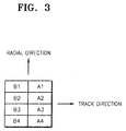
- T1 and T2 track-directional sum signals A+D and B+C are represented as T1 and T2.
- the present invention is not limited to the four-section photodetector.
- T1 can indicate the sum of B1, B2, B3 and B4
- T2 can indicate the sum of A1, A2, A3 and A4.
- one of the detected signals X1 and X2 output by the optical detection device 204 is better than the other due to the direction of defocusing.
- the selector 228 selects the better quality signal from the detected signals X1 and X2 in response to a selection control signal provided from the system state detector 226.
- the fifth or sixth equalizer 238 or 240 which receives the selected detected signal, equalizes the selected detected signal according to the adaptive equalization amount that can compensate for the amount of signal interference caused due to the defocusing detected by the system state detector 226. In this way, an optimal RF reproducing signal is provided.
- one of the detected signals R1 and R2 output by the optical detection device 204 is better than the other due to the direction of detracking.
- the selector 228 selects one of the detected signals R1 and R2 in response to a selection control signal provided from the system state detector 226.
- the first or second equalizer 230 or 232 which receives the selected detected signal, equalizes the selected detected signal according to the adaptive equalization amount that can compensate for the amount of signal interference caused due to the detracking detected by the system state detector 226. In this way, an optimal RF reproducing signal is provided.
- one of the detected signals R1 and R2 output by the optical detection device 204 is better than the other due to radial tilting.
- the selector 228 selects one of the detected signals R1 and R2 in response to a selection control signal provided from the system state detector 226.
- the first or second equalizer 230 or 232 which receives the selected detected signal, equalizes the selected detected signal according to the adaptive equalization amount that can compensate for the amount of signal interference caused due to the radial tilting detected by the system state detector 226. In this way, an optimal RF reproducing signal is provided.
- one of the detected signals T1 and T2 output by the optical detection device 204 is better than the other due to tangential tilting.
- the selector 228 selects one of the detected signals T1 and T2 in response to a selection control signal provided from the system state detector 226.
- the n outputs of an optical detection device which can be an n-section photodetector, are combined and grouped into two parts, depending on the data conditions recorded on a disc, the state of the interference between optical signals reflected/diffracted from pits in close proximity and from adjacent tracks on a recording medium, or system states.
- an optical detection device which can be an n-section photodetector
- the detected signal R1 which is one of the outputs of sections of the photodetector having the same distance from the center of the disk, is better than the detected signal R2, which is another signal output from sections of the photodetector having the same distance from the center of the disk.
- the detected signal R1 is more degraded than the detected signal R2.
- the detected signal that improves the reproducing signal is selected from the two detected signals, in order to prevent degradation of the reproducing signal, resulting in an improvement in reproduction.
- Figure 4 which shows the results of detection of a reproducing signal during detracking
- the jitter values of reproducing signals according to the present invention are compared to that in the prior art.
- the detected signal R2 Upon negative detracking, the detected signal R2 has less jitter than the prior art and the detected signal R1. Thus, in this case, it is preferable that the detected signal R2 is used as a reproducing signal.
- the detected signal R1 Upon positive detracking, the detected signal R1 has less jitter than the prior art and the detected signal R2. Thus, in this case, it is preferable that the detected signal R1 is used as a reproducing signal.
- jitter is about 15.6% (data to data).
- the detected signal R2 when the detected signal R2 is used upon detracking of -0.08 ⁇ m, jitter of about 9.22% is obtained.
- the detected signal R1 is used upon detracking of +0.08 ⁇ m, jitter of about 9.22% is obtained. Therefore, the present invention can obtain a reproducing signal having good characteristics and a wide margin, compared to the prior art.
- Figure 5 which shows the results of detection of a reproducing signal during tangential tilting
- the jitter values of reproducing signals according to the present invention are compared to that in the prior art.
- the detected signal T1 Upon negative tilting, the detected signal T1 has less jitter than the prior art and the detected signal R2. Thus, in this case, it is preferable that the detected signal T1 is used as a reproducing signal.
- the detected signal T2 Upon positive tilting, the detected signal T2 has less jitter than the prior art and the detected signal T1. Thus, in this case, it is preferable that the detected signal T2 is used as a reproducing signal.
- the outputs of an optical detection device which are the least degraded, are used to reproduce a signal, depending on the system states, the data conditions and/or the interference between optical signals reflected/diffracted from pits in close proximity and from adjacent tracks on a recording medium.
- the jitter of a detected signal is improved, and the performance of the system can be improved.
- the demodulation degree of a signal which is the most important factor in signal processing, is improved. Hence, signal distortion and signal degradation are reduced, and the performance of the system can be improved.
- the use of a reproducing signal according to the present invention increases the defocusing margin, the detracking margin, the radial tilting margin, and the tangential tilting margin, so that the performance of the system can be improved.
Landscapes
- Optical Recording Or Reproduction (AREA)
- Signal Processing For Digital Recording And Reproducing (AREA)
Abstract
Description
Claims (13)
- A method of detecting a reproducing signal using an optical detection device (204) for receiving an optical signal reflected from an optical recording medium (200) and dividing the received signal into multiple signals (A,B,C,D) corresponding to sections of the optical detection device (204) which are arranged in a matrix with rows in the tangential direction and columns in the radial direction of the optical recording medium (200), the method comprising the steps of:(a) selecting (228) some signals (e.g. A,B), which are less degraded than other signals (e.g. C,D), from among the output signals (A-D) of the optical detection device (204), on the basis of data conditions recorded on the optical recording medium, the interference between optical signals reflected/diffracted from pits in close proximity and from adjacent tracks on a recording medium, and/or system states; and(b) obtaining (230-240) a reproducing signal from the selected signals by compensating (230-240) for the amount of signal interference caused due to the data conditions, the interference between optical signals reflected/diffracted from pits in close proximity and from adjacent tracks on a recording medium, and/or system states, on the basis of the results of the detection.
- The method of claim 1, wherein in the step (a), one (T1,T2) among the outputs of the optical detection device (204-212) corresponding to a combination of signals (A+D,B+C) corresponding to sections (A-D) of the optical detection device (204) arranged in the radial direction is selected depending on signal interference caused due to data conditions or the interference between optical signals reflected/diffracted from pits in close proximity and from adjacent tracks on a recording medium.
- The method of claim 1, wherein in the step (a), one (X1,X2) among the outputs of the optical detection device (204-212) corresponding to a combination of signals (A+C,B+D) corresponding to sections (A-D) of the optical detection device arranged diagonally is selected depending on signal interference caused due to defocusing.
- The method of claim 1, wherein in the step (a), one (R1,R2) among the outputs of the optical detection device (204-212) corresponding to a combination of signals (A+B,C+D) corresponding to sections (A-D) of the optical detection device (204) arranged in the track direction is selected depending on signal interference caused due to detracking.
- The method of claim 1, wherein in the step (a), one (R1,R2) among the outputs of the optical detection device (204-212) corresponding to a combination of signals (A+B,C+D) corresponding to sections (A-D) of the optical detection device (204) arranged in the track direction is selected depending on signal interference caused due to radial tilting.
- The method of claim 1, wherein in the step (a), one (T1,T2) among the outputs of the optical detection device (204-212) corresponding to a combination of signals (A+D,B+C) corresponding to sections (A-D) of the optical detection device (204) arranged in the radial direction is selected depending on signal interference caused due to tangential tilting.
- The method of any of claims 1 to 6, wherein in the step (b), the selected outputs of the optical detection device are adaptively equalized (230-240) according to the amount of signal interference caused due to the data conditions, the interference between optical signals reflected/diffracted from pits in close proximity and from adjacent tracks on a recording medium, and/or system states.
- The method of any of claims 1 to 7, wherein the reproducing signal is used to increase the defocusing margin of a system and/or is used to increase the detracking margin of a system and/or is used to increase the radial tilting margin of a system and/or is used to increase the tangential tilting margin of a system.
- A method of detecting a reproducing signal using an optical detection device including a photodetecting means (204) for receiving an optical signal reflected from an optical recording medium (200) and dividing the received signal into multiple signals (A-D), the method comprising the steps of:(a) detecting the outputs (R1,R2) of the optical detection device (204) corresponding to a combination of signals corresponding to sections (A-D) of the photodetecting means (204) arranged in the track direction, the outputs (T1,T2) corresponding to a combination of signals corresponding to sections of the photodetecting means arranged in the radial direction, and/or the outputs (X1,X2) corresponding to a combination of signals corresponding to sections of the photodetecting means arranged diagonally; and(b) detecting (226) a good signal among output signals obtained by reproducing the outputs detected in the step (a), as a reproducing signal.
- The method of claim 9, further comprising (c) controlling a good signal to be detected as a reproducing signal in the step (b), by detecting the data conditions recorded on the optical recording medium, the interference between optical signals reflected/diffracted from pits in close proximity and from adjacent tracks on a recording medium, and/or various system states.
- A device for detecting a reproducing signal using an optical detection device including a photodetecting means (204) for receiving an optical signal reflected from an optical recording medium (200) and dividing the received signal into multiple signals (A-D), the device comprising:a detector (214-224) for detecting the outputs (R1,R2) of the optical detection device corresponding to a combination of signals corresponding to sections of the photodetecting means arranged in the track direction, the outputs (T1,T2) corresponding to a combination of signals corresponding to sections of the photodetecting means arranged in the radial direction, and/or the outputs (X1,X2) corresponding to a combination of signals corresponding to sections of the photodetecting means arranged diagonally;a control unit (226) for providing a selection control signal and a compensation signal on the basis of the results of detection of the data conditions recorded on the optical recording medium, the interference between optical signals reflected/diffracted from pits in close proximity and from adjacent tracks on a recording medium, and/or various system states; anda compensator (228,230-240) for selecting some of the outputs of the optical detection device provided via the detector in response to the selection control signal, and adaptively compensating for the selected outputs in response to the compensation signal.
- The device of claim 11, wherein the compensator (228,230-240) comprises:a selector (228) for selecting some of the outputs of the optical detection device provided via the detector (214-224) in response to the selection control signal; andan equalizer (230-240) for adaptively equalizing the selected outputs of the optical detection device in response to the compensation signal.
- A device for detecting a reproducing signal using an optical detection device including a photodetecting means (204) for receiving an optical signal reflected from an optical recording medium (200) and dividing the received signal into multiple signals (A-D), the device comprising:a detector (214-224) for detecting the outputs (R1,R2) of the optical detection device corresponding to a combination of signals corresponding to sections of the photodetecting means (204) arranged in the track direction, the outputs (T1,T2) corresponding to a combination of signals corresponding to sections of the photodetecting means arranged in the radial direction, and/or the outputs (X1,X2) corresponding to a combination of signals corresponding to sections of the photodetecting means arranged diagonally;an equalizer (230-240) for equalizing and reproducing each of the outputs of the detector; anda control unit (226) for adaptively controlling the equalization amount of the equalizer on the basis of the results of detection of the data conditions recorded on the optical recording medium, the interference between optical signals reflected/diffracted from pits in close proximity and from adjacent tracks on a recording medium, and/or various system states, and providing a good signal, among the output signals of the equalizer, as a reproducing signal.
Applications Claiming Priority (2)
| Application Number | Priority Date | Filing Date | Title |
|---|---|---|---|
| KR9940647 | 1999-09-21 | ||
| KR1019990040647A KR100708066B1 (en) | 1999-09-21 | 1999-09-21 | Playback signal detection method and apparatus |
Publications (3)
| Publication Number | Publication Date |
|---|---|
| EP1087382A2 true EP1087382A2 (en) | 2001-03-28 |
| EP1087382A3 EP1087382A3 (en) | 2003-01-29 |
| EP1087382B1 EP1087382B1 (en) | 2005-03-16 |
Family
ID=19612428
Family Applications (1)
| Application Number | Title | Priority Date | Filing Date |
|---|---|---|---|
| EP00308236A Expired - Lifetime EP1087382B1 (en) | 1999-09-21 | 2000-09-20 | Method of detecting a reproduction signal and circuit therefor |
Country Status (7)
| Country | Link |
|---|---|
| US (1) | US6914860B1 (en) |
| EP (1) | EP1087382B1 (en) |
| JP (1) | JP2001110058A (en) |
| KR (1) | KR100708066B1 (en) |
| CN (1) | CN1198268C (en) |
| DE (1) | DE60018664T2 (en) |
| TW (1) | TW526484B (en) |
Families Citing this family (1)
| Publication number | Priority date | Publication date | Assignee | Title |
|---|---|---|---|---|
| KR100457518B1 (en) * | 2002-05-07 | 2004-11-17 | 삼성전자주식회사 | Apparatus and method for compensating tilt |
Family Cites Families (14)
| Publication number | Priority date | Publication date | Assignee | Title |
|---|---|---|---|---|
| US4536866A (en) * | 1978-11-30 | 1985-08-20 | Videonics Of Hawaii, Inc. | Information retrieval system and apparatus |
| JPS61222033A (en) | 1985-03-28 | 1986-10-02 | Matsushita Electric Ind Co Ltd | Optical recording and reproducing device |
| JPS61248240A (en) | 1985-04-26 | 1986-11-05 | Matsushita Electric Ind Co Ltd | Optical recording and reproducing device |
| JPH01122041A (en) | 1987-11-06 | 1989-05-15 | Hitachi Ltd | optical information pickup |
| JP2614482B2 (en) * | 1988-03-11 | 1997-05-28 | 三洋電機株式会社 | Signal reproduction circuit of optical disc player |
| US5255262A (en) * | 1991-06-04 | 1993-10-19 | International Business Machines Corporation | Multiple data surface optical data storage system with transmissive data surfaces |
| JP3066118B2 (en) | 1991-07-19 | 2000-07-17 | パイオニア株式会社 | Photodetector |
| JP3070783B2 (en) | 1991-10-29 | 2000-07-31 | ソニー株式会社 | Optical disk device |
| JPH05242512A (en) | 1991-12-19 | 1993-09-21 | Matsushita Electric Ind Co Ltd | Optical disk device |
| US5483515A (en) * | 1994-09-16 | 1996-01-09 | International Business Machines Corporation | Apparatus and method for cancelling cross-talk in signals from optical data storage systems |
| JP3447135B2 (en) * | 1995-02-02 | 2003-09-16 | パイオニア株式会社 | Information playback device |
| US5701283A (en) * | 1995-11-15 | 1997-12-23 | Zen Research N.V. | Method and apparatus for high speed optical storage device |
| US5978322A (en) * | 1996-07-30 | 1999-11-02 | Kabushiki Kaisha Toshiba | Optical recording medium having a parameter for identifying the format of data and a reproducing device thereof |
| JPH1097765A (en) | 1996-07-30 | 1998-04-14 | Toshiba Corp | Recording medium, its reproducing apparatus, data reproducing apparatus and data reproducing method |
-
1999
- 1999-09-21 KR KR1019990040647A patent/KR100708066B1/en not_active Expired - Fee Related
-
2000
- 2000-09-19 JP JP2000284112A patent/JP2001110058A/en active Pending
- 2000-09-20 DE DE60018664T patent/DE60018664T2/en not_active Expired - Lifetime
- 2000-09-20 EP EP00308236A patent/EP1087382B1/en not_active Expired - Lifetime
- 2000-09-21 US US09/666,857 patent/US6914860B1/en not_active Expired - Fee Related
- 2000-09-21 CN CNB001287796A patent/CN1198268C/en not_active Expired - Fee Related
-
2001
- 2001-03-01 TW TW089119410A patent/TW526484B/en not_active IP Right Cessation
Also Published As
| Publication number | Publication date |
|---|---|
| CN1289115A (en) | 2001-03-28 |
| EP1087382A3 (en) | 2003-01-29 |
| DE60018664T2 (en) | 2005-08-11 |
| US6914860B1 (en) | 2005-07-05 |
| EP1087382B1 (en) | 2005-03-16 |
| JP2001110058A (en) | 2001-04-20 |
| DE60018664D1 (en) | 2005-04-21 |
| CN1198268C (en) | 2005-04-20 |
| KR20010028414A (en) | 2001-04-06 |
| TW526484B (en) | 2003-04-01 |
| KR100708066B1 (en) | 2007-04-16 |
Similar Documents
| Publication | Publication Date | Title |
|---|---|---|
| US7046595B2 (en) | Method of reproducing information with equalization coefficient for the reproduced information | |
| US7349321B2 (en) | Information reproduction apparatus and information reproduction method | |
| US20120243393A1 (en) | Optical information recording method, optical information reproduction method and optical disk device | |
| US6272105B1 (en) | Optical disc and optical disc reproducing apparatus | |
| US5596559A (en) | Information reproducing apparatus for reproducing digital information by self-clock scheme | |
| EP1087382B1 (en) | Method of detecting a reproduction signal and circuit therefor | |
| KR100289726B1 (en) | Apparatus for reducing inter symbol interference and/or crosstalk, and method thereof | |
| JPH1031824A (en) | Optical pickup device | |
| US6400658B1 (en) | DVD-RAM disk reproduction apparatus for reducing errors during detection of identification data | |
| JP3556881B2 (en) | Reproduction signal detection method and circuit for compensating for time delay | |
| US5666339A (en) | Optical information reproducing apparatus using transversal filter | |
| JP4234042B2 (en) | Multi-value information recording medium, multi-value information waveform equalizer, multi-value information reproducing device | |
| US5726963A (en) | Information reproduction apparatus including a phase compensation circuit for eliminating the influence of AC-coupling | |
| JPH07254156A (en) | Optical disk and signal processing circuit of optical disk reproducing device | |
| JP3941220B2 (en) | Optical disk playback device | |
| JP7774201B2 (en) | Information recording/reproducing apparatus and information recording/reproducing method | |
| JP3011230B2 (en) | Optical disc playback device | |
| KR100297772B1 (en) | Method and apparatus for playing disk | |
| KR100299987B1 (en) | Dvd-ram disk player for reducing error in id data detection | |
| US20080205208A1 (en) | Optical System With Filtered Push Pull Radial Tracking | |
| JPH0831093A (en) | Optical disc medium and device | |
| JPH0573915A (en) | Optical recording / reproducing device | |
| JPH09306103A (en) | Intercode interference reducing device in optical pickup device | |
| JPH087292A (en) | Optical disc media | |
| JPH0612699A (en) | Optical recording medium |
Legal Events
| Date | Code | Title | Description |
|---|---|---|---|
| PUAI | Public reference made under article 153(3) epc to a published international application that has entered the european phase |
Free format text: ORIGINAL CODE: 0009012 |
|
| 17P | Request for examination filed |
Effective date: 20001004 |
|
| AK | Designated contracting states |
Kind code of ref document: A2 Designated state(s): AT BE CH CY DE DK ES FI FR GB GR IE IT LI LU MC NL PT SE |
|
| AX | Request for extension of the european patent |
Free format text: AL;LT;LV;MK;RO;SI |
|
| RIN1 | Information on inventor provided before grant (corrected) |
Inventor name: OTSUKA, TATSUHIRO Inventor name: LEE, KYUNG-GEUN Inventor name: JOO, SEONG-SIN |
|
| PUAL | Search report despatched |
Free format text: ORIGINAL CODE: 0009013 |
|
| AK | Designated contracting states |
Designated state(s): AT BE CH CY DE DK ES FI FR GB GR IE IT LI LU MC NL PT SE |
|
| AX | Request for extension of the european patent |
Extension state: AL LT LV MK RO SI |
|
| RIC1 | Information provided on ipc code assigned before grant |
Ipc: 7G 11B 7/005 B Ipc: 7G 11B 7/00 A Ipc: 7G 11B 20/10 B |
|
| 17Q | First examination report despatched |
Effective date: 20030318 |
|
| AKX | Designation fees paid |
Designated state(s): DE FR GB NL |
|
| GRAP | Despatch of communication of intention to grant a patent |
Free format text: ORIGINAL CODE: EPIDOSNIGR1 |
|
| GRAS | Grant fee paid |
Free format text: ORIGINAL CODE: EPIDOSNIGR3 |
|
| GRAA | (expected) grant |
Free format text: ORIGINAL CODE: 0009210 |
|
| AK | Designated contracting states |
Kind code of ref document: B1 Designated state(s): DE FR GB NL |
|
| REG | Reference to a national code |
Ref country code: GB Ref legal event code: FG4D |
|
| REG | Reference to a national code |
Ref country code: IE Ref legal event code: FG4D |
|
| REF | Corresponds to: |
Ref document number: 60018664 Country of ref document: DE Date of ref document: 20050421 Kind code of ref document: P |
|
| PLBE | No opposition filed within time limit |
Free format text: ORIGINAL CODE: 0009261 |
|
| STAA | Information on the status of an ep patent application or granted ep patent |
Free format text: STATUS: NO OPPOSITION FILED WITHIN TIME LIMIT |
|
| ET | Fr: translation filed | ||
| 26N | No opposition filed |
Effective date: 20051219 |
|
| PGFP | Annual fee paid to national office [announced via postgrant information from national office to epo] |
Ref country code: NL Payment date: 20140827 Year of fee payment: 15 Ref country code: DE Payment date: 20140826 Year of fee payment: 15 |
|
| PGFP | Annual fee paid to national office [announced via postgrant information from national office to epo] |
Ref country code: GB Payment date: 20140826 Year of fee payment: 15 Ref country code: FR Payment date: 20140825 Year of fee payment: 15 |
|
| REG | Reference to a national code |
Ref country code: DE Ref legal event code: R119 Ref document number: 60018664 Country of ref document: DE |
|
| GBPC | Gb: european patent ceased through non-payment of renewal fee |
Effective date: 20150920 |
|
| REG | Reference to a national code |
Ref country code: NL Ref legal event code: MM Effective date: 20151001 |
|
| REG | Reference to a national code |
Ref country code: FR Ref legal event code: ST Effective date: 20160531 |
|
| PG25 | Lapsed in a contracting state [announced via postgrant information from national office to epo] |
Ref country code: GB Free format text: LAPSE BECAUSE OF NON-PAYMENT OF DUE FEES Effective date: 20150920 Ref country code: DE Free format text: LAPSE BECAUSE OF NON-PAYMENT OF DUE FEES Effective date: 20160401 |
|
| PG25 | Lapsed in a contracting state [announced via postgrant information from national office to epo] |
Ref country code: NL Free format text: LAPSE BECAUSE OF NON-PAYMENT OF DUE FEES Effective date: 20151001 Ref country code: FR Free format text: LAPSE BECAUSE OF NON-PAYMENT OF DUE FEES Effective date: 20150930 |