EP1085647A2 - Compensation circuit, method of operation thereof and converter employing the same - Google Patents
Compensation circuit, method of operation thereof and converter employing the same Download PDFInfo
- Publication number
- EP1085647A2 EP1085647A2 EP00307640A EP00307640A EP1085647A2 EP 1085647 A2 EP1085647 A2 EP 1085647A2 EP 00307640 A EP00307640 A EP 00307640A EP 00307640 A EP00307640 A EP 00307640A EP 1085647 A2 EP1085647 A2 EP 1085647A2
- Authority
- EP
- European Patent Office
- Prior art keywords
- signal
- converter
- output
- ramp
- modulator
- Prior art date
- Legal status (The legal status is an assumption and is not a legal conclusion. Google has not performed a legal analysis and makes no representation as to the accuracy of the status listed.)
- Withdrawn
Links
Images



Classifications
-
- H—ELECTRICITY
- H02—GENERATION; CONVERSION OR DISTRIBUTION OF ELECTRIC POWER
- H02M—APPARATUS FOR CONVERSION BETWEEN AC AND AC, BETWEEN AC AND DC, OR BETWEEN DC AND DC, AND FOR USE WITH MAINS OR SIMILAR POWER SUPPLY SYSTEMS; CONVERSION OF DC OR AC INPUT POWER INTO SURGE OUTPUT POWER; CONTROL OR REGULATION THEREOF
- H02M3/00—Conversion of DC power input into DC power output
- H02M3/22—Conversion of DC power input into DC power output with intermediate conversion into AC
- H02M3/24—Conversion of DC power input into DC power output with intermediate conversion into AC by static converters
- H02M3/28—Conversion of DC power input into DC power output with intermediate conversion into AC by static converters using discharge tubes with control electrode or semiconductor devices with control electrode to produce the intermediate AC
- H02M3/325—Conversion of DC power input into DC power output with intermediate conversion into AC by static converters using discharge tubes with control electrode or semiconductor devices with control electrode to produce the intermediate AC using devices of a triode or a transistor type requiring continuous application of a control signal
- H02M3/335—Conversion of DC power input into DC power output with intermediate conversion into AC by static converters using discharge tubes with control electrode or semiconductor devices with control electrode to produce the intermediate AC using devices of a triode or a transistor type requiring continuous application of a control signal using semiconductor devices only
- H02M3/33507—Conversion of DC power input into DC power output with intermediate conversion into AC by static converters using discharge tubes with control electrode or semiconductor devices with control electrode to produce the intermediate AC using devices of a triode or a transistor type requiring continuous application of a control signal using semiconductor devices only with automatic control of the output voltage or current, e.g. flyback converters
-
- H—ELECTRICITY
- H02—GENERATION; CONVERSION OR DISTRIBUTION OF ELECTRIC POWER
- H02M—APPARATUS FOR CONVERSION BETWEEN AC AND AC, BETWEEN AC AND DC, OR BETWEEN DC AND DC, AND FOR USE WITH MAINS OR SIMILAR POWER SUPPLY SYSTEMS; CONVERSION OF DC OR AC INPUT POWER INTO SURGE OUTPUT POWER; CONTROL OR REGULATION THEREOF
- H02M3/00—Conversion of DC power input into DC power output
- H02M3/22—Conversion of DC power input into DC power output with intermediate conversion into AC
- H02M3/24—Conversion of DC power input into DC power output with intermediate conversion into AC by static converters
- H02M3/28—Conversion of DC power input into DC power output with intermediate conversion into AC by static converters using discharge tubes with control electrode or semiconductor devices with control electrode to produce the intermediate AC
- H02M3/325—Conversion of DC power input into DC power output with intermediate conversion into AC by static converters using discharge tubes with control electrode or semiconductor devices with control electrode to produce the intermediate AC using devices of a triode or a transistor type requiring continuous application of a control signal
- H02M3/335—Conversion of DC power input into DC power output with intermediate conversion into AC by static converters using discharge tubes with control electrode or semiconductor devices with control electrode to produce the intermediate AC using devices of a triode or a transistor type requiring continuous application of a control signal using semiconductor devices only
- H02M3/33569—Conversion of DC power input into DC power output with intermediate conversion into AC by static converters using discharge tubes with control electrode or semiconductor devices with control electrode to produce the intermediate AC using devices of a triode or a transistor type requiring continuous application of a control signal using semiconductor devices only having several active switching elements
Definitions
- the present invention is directed, in general, to power conversion and, more specifically, to a compensation circuit for a switched-mode power converter, a method of compensating for a change in an output characteristic of the converter and a converter employing the circuit or the method.
- a power converter is a power processing circuit that converts an input voltage waveform into a specified output voltage waveform.
- Switched-mode power converters generally include an inverter, a transformer having a primary winding coupled to the inverter, a rectifier coupled to a secondary winding of the transformer, an output filter and a controller.
- the inverter generally includes a power switch, such as a field-effect transistor (FET), that converts an input voltage to a switched voltage that is applied across the transformer.
- FET field-effect transistor
- the transformer then transforms the voltage to another value and the rectifier generates a desired voltage at the output of the converter.
- the output filter typically an output inductor and an output capacitor, smooths and filters the output voltage for delivery to a load.
- the controller typically includes an error amplifier coupled to the output of the power converter.
- the controller further includes a modulator coupled between the error amplifier and the power switch.
- the error amplifier monitors the output voltage of the power converter and generates an error signal representing a deviation between the actual output voltage and a desired output voltage.
- the modulator then generates a drive signal for the power switch based on the error signal. For example, the drive signal may maintain the power switch in a conduction mode while the error signal exceeds a periodic ramp signal. The drive signal may then transition the power switch to a non-conduction mode when the periodic ramp signal reaches the error signal.
- a current in the power converter such as a switch current through the power switch or an inductor current through the output inductor, is substituted for, or added to, the periodic ramp signal.
- the output voltage of the converter is still fed back through the error amplifier circuit to provide a component of the error signal for the modulator.
- the switching cycle may be divided into a primary interval D (during which the power switch is in the conduction mode) and an auxiliary interval 1-D (during which the power switch is in the non-conduction mode).
- the primary interval D begins with a timing circuit resetting the ramp signal to the modulator, causing the modulator to place the power switch in the conduction mode.
- the ramp signal continues to rise at substantially constant slope.
- the power switch is placed in the non-conduction mode to begin the auxiliary interval 1-D.
- the modulator simply waits for the timing circuit to reset the ramp signal to begin a new switching cycle.
- the modulator thus exhibits an active decision process during the primary interval D. Any change in the error signal either continues to keep the power switch in the conduction mode (because the error signal is greater than the ramp signal) or places the power switch in the non-conduction mode thereby ending the primary interval D (because the error signal has dropped below the ramp signal). During the auxiliary interval 1-D, however, the modulator must wait for the timing circuit to begin the new switching cycle. Any change in the error signal resulting from changes in the operating conditions of the power converter is effectively ignored, thereby limiting the response of the power converter.
- the present invention provides, for use with a switched-mode power converter having a modulator that develops a drive signal for a power switch, a compensation circuit, a method of compensating for a change in an output characteristic of the converter and a converter employing the circuit or the method.
- the compensation circuit includes (1) a sensor that senses an output characteristic of the converter and (2) a filter, coupled to the sensor, that develops an intermediate signal representing a change in the output characteristic.
- the modulator adjusts a switching period of the drive signal as a function of the intermediate signal thereby to decrease a reaction delay of the converter.
- the present invention in one aspect, introduces the broad concept of reducing a reaction delay of a converter to a change in an output characteristic (e.g ., an output voltage or an output current) of the converter.
- the present invention recognizes that the converter may be employed to power loads requiring fast, large amplitude changes in, for example, output current.
- the present invention further recognizes that changes occurring during an auxiliary interval of the power switch (when the power switch is in a non-conduction mode) may not be effectively addressed until the beginning of a new switching cycle.
- the present invention thus advantageously employs the compensation circuit to allow the modulator to adjust the switching period of the drive signal, as well as a duty cycle of the power switch, thereby decreasing a reaction delay of the converter to the change in the output characteristic.
- the modulator includes a switching cycle comparator that modifies the ramp signal as a function of the intermediate signal.
- the modulator may thus adjust the switching period as a function of the ramp signal.
- the switching cycle comparator modifies the ramp signal by resetting the ramp signal.
- the switching cycle comparator modifies the ramp signal by changing a slope of the ramp signal.
- the converter further has a ramp generator that generates a ramp signal and an error amplifier that compares the output voltage to a reference voltage and develops therefrom an error signal.
- the modulator may thus include a duty cycle comparator that receives the ramp signal and the error signal and develops therefrom the drive signal.
- the compensation circuit further includes an error amplifier that compares the output voltage to a reference voltage and develops therefrom an error signal. The filter may thus develop the intermediate signal as a function of a change in the error signal.
- the senor includes an observer circuit, parallel-coupled to the output capacitor, that develops an output current signal representing the output current.
- the filter may thus develop the intermediate signal as a function of the output current signal.
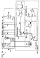
- the power converter 100 includes an inverter 110 coupled to an input of the power converter 100.
- the power converter 100 further includes a transformer T 1 having a primary winding S 1 , coupled to the inverter 110, and a secondary winding S 2 .
- the power converter 100 further includes a rectifier 120, coupled to the secondary winding S 2 , that rectifies a periodic AC waveform supplied by the secondary winding S 2 .
- the power converter 100 further includes an output filter 130 coupled to the rectifier 120.
- the output filter 130 filters the rectified waveform from the rectifier 120 to supply an output voltage V OUT to a load 190 at an output of the power converter 100.
- the power converter 100 still further includes a controller 140, coupled to the inverter 110, that monitors the output voltage V OUT and adjusts the switching of the inverter 110 to maintain the output voltage V OUT at a substantially constant level.
- the inverter 110 includes a power switch Q 1 coupled to the input of the power converter 100.
- the controller 140 intermittently switches the power switch Q 1 to apply a DC input voltage V IN across the primary winding S 1 .
- the inverter 110 includes a clamping circuit (having a clamping switch Q 2 and a clamping capacitor C CLAMP ) to reset the flux in the transformer T 1 during the off period of the power switch Q 1 . While the embodiment illustrated and described shows a generic inverter 110, those skilled in the art will realize that the principles of the present invention may be employed with a wide variety of inverter topologies.
- the rectifier 120 includes first and second rectifier diodes D 1 , D 2 arranged in a forward topology.
- the output filter 130 includes a filter capacitor C F coupled across the output of the power converter 100.
- the output filter 130 further includes a filter inductor L F coupled to the filter capacitor C F .
- the controller 140 includes a ramp generator 145, a compensation circuit 160 and a modulator 150.
- the ramp generator 145 includes a current source I RAMP coupled to a timing switch Q TS .
- the ramp generator 145 further includes a timing capacitor C T coupled across the timing switch Q TS .
- the current source I RAMP provides a current to charge the timing capacitor C T , causing the ramp signal V RAMP to rise.
- the timing switch Q TS turns on briefly to discharge the timing capacitor C T and reset the ramp signal V RAMP .
- the timing switch Q TS then turns off to allow the current source I RAMP to recharge the timing capacitor C T , thereby initiating another switching cycle.
- the compensation circuit 160 is coupled between the output of the power converter 100 and the modulator 150.
- the compensation circuit 160 includes a sensor 170, an error amplifier 175 and a filter 180.
- the sensor 170 is coupled to the output of the power converter 100 to sense an output characteristic thereof.
- the output characteristic is the output voltage V OUT .
- the sensor 170 includes a voltage scaling circuit having first and second voltage scaling resistors R1, R2. The voltage scaling circuit scales the output voltage V OUT to develop a scaled output voltage.
- Those skilled in the art are familiar with voltage scaling circuits. Of course, other types of voltage and current sensors are well within the broad scope of the present invention.
- the error amplifier 175 is coupled to the sensor 170 and receives the scaled output voltage therefrom.
- the error amplifier 175 compares the scaled output voltage to a reference voltage V REF1 and develops therefrom an error signal V TH representing a scaled difference between a desired output voltage (represented by the reference voltage V REF1 ) and the actual output voltage V OUT .
- the reference voltage V REF1 may include a signal representing an output current I OUT or another parameter of the power converter 100.
- the filter 180 receives the error signal V TH and develops therefrom an intermediate signal V INT that preferably represents a change in the output characteristic (such as the output voltage V OUT ) of the power converter 100.
- the filter 180 may be represented by the following equation. Ks ( ⁇ 1 s +1)( ⁇ 2 s +1)
- Filter refers to a class of circuits, including passive and active filters, that is capable of transforming a characteristic of a signal ( e.g ., differentiation, integration, low pass filtering).
- the modulator 150 is coupled to the compensation circuit 160 and the ramp generator 145.
- the modulator 150 includes a switching cycle comparator 152, a duty cycle comparator 154, a summer 156 and a drive circuit 158 for driving the clamping switch Q 2 .
- the summer 156 is coupled to the filter 180 and receives the intermediate signal V INT therefrom.
- the summer 156 combines the intermediate signal V INT and a second reference voltage V REF2 to produce a switching cycle termination signal V SCT that is delivered to the switching cycle comparator 152.
- the second reference voltage V REF2 may be set at a level sufficient to provide a base switching frequency.
- the switching cycle comparator 152 receives the switching cycle termination signal V SCT and modifies the ramp signal V RAMP as a function thereof. In the illustrated embodiment, the switching cycle comparator 152 compares the switching cycle termination signal V SCT to the ramp signal V RAMP to determine an appropriate time to turn on the timing switch Q TS and thereby reset the ramp signal V RAMP .
- the switching cycle comparator 152 compares the switching cycle termination signal V SCT to the ramp signal V RAMP to determine an appropriate time to turn on the timing switch Q TS and thereby reset the ramp signal V RAMP .
- other methods of modifying the ramp signal V RAMP e.g ., changing a slope of the ramp signal V RAMP ) are well within the broad scope of the present invention.
- the duty cycle comparator 154 compares the error signal V TH to the ramp signal V RAMP and develops therefrom a drive signal for driving the power switch Q 1 .
- the drive circuit 158 may, in one embodiment, invert the drive signal to develop a signal for driving the clamping switch Q 2 .
- the duty cycle comparator 154 may thus establish a primary interval D (during which the power switch Q 1 is in the conduction mode) and an auxiliary interval 1-D (during which the power switch Q 1 is in the non-conduction mode).
- the switching cycle comparator 152 may thus adjust the switching period of the power switch Q 1 as a function of the intermediate signal V INT .
- the compensation circuit 160 therefore, may decrease a reaction delay of the power converter 100 to, for instance, a change in the output characteristic (such as the output voltage V OUT or output current I OUT ).
- FIGURE 1B illustrated are graphical representations of waveforms associated with the power converter 100 of FIGURE 1A.
- the operation of the power converter 100 will therefore be discussed with continuing reference to FIGUREs 1A and 1B.
- a fast, large amplitude step change in the output current I OUT generated by the load 190 causes a sudden drop in the output voltage V OUT .
- the error signal V TH developed by comparing the output voltage V OUT to the reference voltage V REF1 , increases to indicate an increase in a scaled difference between the desired output voltage and the actual output voltage V OUT .
- An increase in the error signal V TH causes the duty cycle comparator 154 to accordingly increase a period of the primary interval D such that the error signal V TH may be reduced to a nominal level.
- the filter 180 receives the error signal V TH and develops therefrom the intermediate signal V INT , which is combined with the second reference voltage V REF2 to produce the switching cycle termination signal V SCT .
- the switching cycle termination signal V SCT decreases. Since the primary interval D ends when the ramp signal V RAMP has risen to a level substantially equal to the switching cycle termination signal V SCT , the decrease in the switching cycle termination signal V SCT may thus allow the auxiliary interval 1-D to be shortened or terminated in response to, for example, an increase in the load current I OUT that causes a corresponding decrease in the output voltage V OUT .
- the controller 140 may thus operate during both the primary interval D and the auxiliary interval 1-D.
- FIGURE 2A illustrated is a schematic diagram of another embodiment of a power converter 200 constructed in accordance with the principles of the present invention.
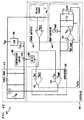
- the power converter 200 includes a power train 210 and a controller 240.
- the power train 210 receives an input voltage V IN and supplies an output voltage V OUT to a load 290 at an output of the power converter 200.
- the controller 240 includes an error amplifier 242, a ramp generator 245, a compensation circuit 260 and a modulator 250.
- the error amplifier 242 is coupled to the output of the power converter 200 and the modulator 250.
- the error amplifier 242 includes a voltage sensor (e.g ., a voltage divider) 244 that develops a scaled output voltage.
- the error amplifier 242 compares the scaled output voltage to a reference voltage V REF1 and develops therefrom an error signal V TH representing a scaled difference between a desired output voltage (represented by the reference voltage V REF1 ) and the actual output voltage V OUT .
- the ramp generator 245 includes a current source I RAMP coupled to a timing switch Q TS .
- the ramp generator 245 further includes a timing capacitor C T coupled across the timing switch Q TS .
- the ramp generator 245 is analogous to the ramp generator 145 described with respect to FIGURE 1A and will not be further described.
- the compensation circuit 260 includes a sensor 270, coupled to an output of the power converter 200, that senses an output characteristic of the power converter 200.
- the output characteristic is an output current I OUT .
- the sensor 270 includes a current sensor coupled between the output of the power converter 200 and the load 290.
- the sensor 270 may include an observer circuit, parallel-coupled to an output capacitor (or an output inductor) of the power converter 200, that develops an output current signal representing the output current I OUT .
- the compensation circuit 260 further includes a filter 280 coupled to the sensor 270.
- the filter 280 develops an intermediate signal V INT representing a change in the output current I OUT of the power converter 200.
- the modulator 250 is coupled to the ramp generator 245, the compensation circuit 260 and the error amplifier 242.
- the modulator 250 includes a switching cycle comparator 252, a duty cycle comparator 254 and a summer 256.
- the modulator 250 is analogous to the modulator 150 illustrated and described with respect to the power converter 100 of FIGURE 1A and, as a result, will not be described in detail.
- the modulator 250 receives the intermediate signal V INT from the compensation circuit 260 and adjusts the switching period of the drive signal as a function thereof, thereby decreasing a reaction delay of the power converter 200 to fast, large amplitude step changes in the output current I OUT .
- the load 290 may require a fast, large amplitude step change in the output current I OUT .
- the filter 280 receives the output current signal (representing the output current I OUT ) from the sensor 270 and develops therefrom the intermediate signal V INT .
- the intermediate signal V INT is then combined with the second reference voltage V REF2 to produce the switching cycle termination signal V SCT .
- the switching cycle termination signal V SCT may be employed to shorten or terminate the auxiliary interval 1-D in response to fast, large amplitude step change in the output current I OUT .
- FIGURE 3A illustrated is a schematic diagram of another embodiment of a power converter 300 constructed in accordance with the principles of the present invention.
- the power converter 300 includes a power train 310 and a controller 340.
- the power train 310 receives an input voltage V IN and supplies an output voltage V OUT to a load 390 at an output of the power converter 300.
- the controller 340 includes an error amplifier 342, a ramp generator 345, a compensation circuit 360 and a modulator 350.
- the error amplifier 342 is coupled to the output of the power converter 300 and the modulator 350.
- the error amplifier 342 is analogous to the error amplifier 242 illustrated and described with respect to FIGURE 2A and, as a result, will not be described.
- the ramp generator 345 includes a current source I RAMP coupled to a timing switch Q TS .
- the ramp generator 345 further includes a timing capacitor C T coupled across the timing switch Q TS .
- the ramp generator 345 still further includes a ramp reset comparator 347 coupled (via a first diode D 1 ) to the timing switch Q TS .
- the current source I RAMP provides a current to charge the timing capacitor C T , causing the ramp signal V RAMP to rise.
- the ramp reset comparator 347 ends the switching cycle by briefly turning on the timing switch Q TS to discharge the timing capacitor C T and reset the ramp signal V RAMP .
- the timing switch Q TS then turns off to allow the current source I RAMP to recharge the timing capacitor C T , thereby initiating another switching cycle.
- the compensation circuit 360 includes a sensor 370, coupled to an output of the power converter 300, that senses an output current I OUT of the power converter 300.
- the compensation circuit 360 further includes a filter 380 coupled to the sensor 370.
- the filter 380 develops an intermediate signal V INT representing a change in the output current I OUT of the power converter 300.
- the modulator 350 is coupled to the ramp generator 345, the compensation circuit 360 and the error amplifier 342.
- the modulator 350 includes a switching cycle comparator 352, a duty cycle comparator 354 and an AND circuit 356.
- the modulator 350 receives the intermediate signal V INT from the compensation circuit 360 and adjusts the switching period of the drive signal as a function thereof, thereby decreasing a reaction delay of the power converter 300 to fast, large amplitude step changes in the output current I OUT .
- the AND circuit 356 allows the switching cycle comparator 352 to adjust the switching period of the drive signal by terminating the switching cycle only during an auxiliary interval 1-D (when the power switch Q 1 is in a non-conduction mode).
- the AND circuit 356 may be omitted to allow the switching cycle comparator 352 to terminate the switching cycle without regard to the portion of the switching cycle ( i.e ., primary interval D or auxiliary interval 1-D).
- FIGURE 3B illustrated are graphical representations of waveforms associated with the power converter 300 of FIGURE 3A.
- the operation of the power converter 300 will therefore be discussed with continuing reference to FIGUREs 3A and 3B.
- the load 390 may require a fast, large amplitude step change in the output current I OUT .
- the filter 380 receives the output current signal (representing the output current I OUT ) from the sensor 370 and develops therefrom the intermediate signal V INT .
- the intermediate signal V INT is then compared with the second reference voltage V REF2 to provide a signal to the AND circuit 356.
- the AND circuit 356 allows the switching cycle comparator 352 to shorten or terminate the period of the auxiliary interval 1-D (when the power switch Q 1 is in the non-conduction mode).
- FIGURE 4A illustrated is a schematic diagram of yet another embodiment of a power converter 400 constructed in accordance with the principles of the present invention.
- the power converter 400 includes a power train 410 (illustrated as a buck converter) and a controller 440.
- the power train 410 receives an input voltage V IN and supplies an output voltage V OUT to a load 490 at an output of the power converter 400. While the power train 410 is illustrated as a buck converter, those skilled in the pertinent art realize that the principles of the present invention are applicable to a variety of converter topologies, including forward, flyback and buck-boost topologies.
- the controller 440 includes an error amplifier 442, a ramp generator 445, a compensation circuit 460 and a modulator 450.
- the error amplifier 442 is coupled to the output of the power converter 400 and the modulator 450.
- the error amplifier 442 includes a voltage sensor (e.g ., a voltage divider) 444 that develops a scaled output voltage.
- the error amplifier 442 compares the scaled output voltage to a reference voltage V REF1 and develops therefrom an error signal V TH representing a scaled difference between a desired output voltage (represented by the reference voltage V REF1 ) and the actual output voltage V OUT .
- the ramp generator 445 includes a current source I RAMP coupled to a timing switch Q TS .
- the ramp generator 445 further includes a first timing capacitor C T1 coupled across the timing switch Q TS .
- the ramp generator 445 further includes a series-coupled second timing capacitor C T2 and slope modification switch Q SLOPE , coupled across the timing switch Q TS .
- the slope modification switch Q SLOPE is on and the current source I RAMP provides a current to charge both the first and second timing capacitors C T1 , C T2 to cause the ramp signal V RAMP to rise.
- the timing switch Q TS turns on briefly to discharge the first and second timing capacitors C T1 , C T2 and reset the ramp signal V RAMP .
- the timing switch Q TS then turns off to allow the current source I RAMP to recharge the timing capacitor C T , thereby initiating another switching cycle.
- the compensation circuit 460 includes a sensor 470, coupled to an output of the power converter 400, that senses an output current I OUT of the power converter 400.
- the compensation circuit 460 further includes a filter 480 coupled to the sensor 470.
- the filter 480 develops an intermediate signal V INT representing a change in the output current I OUT of the power converter 400.
- the modulator 450 is coupled to the ramp generator 445, the compensation circuit 460 and the error amplifier 442.
- the modulator 450 includes a switching cycle comparator 452 and a duty cycle comparator 454.
- the modulator 450 receives the intermediate signal V INT from the compensation circuit 460 and operates the slope modification switch Q SLOPE in response thereto.
- the modulator 450 may turn off the slope modification switch Q SLOPE in response to a fast, large amplitude step change in the output current I OUT .
- the modulator 450 may thus change the switching frequency of the ramp signal V RAMP to thereby decrease a reaction delay of the power converter 400 to fast, large amplitude step changes in the output current I OUT .
- the slope of the ramp signal V RAMP may be modified by adjusting the current source I RAMP in response to the intermediate signal V INT .
- FIGURE 4B illustrated are graphical representations of waveforms associated with the power converter 400 of FIGURE 4A.
- the operation of the power converter 400 will therefore be discussed with continuing reference to FIGUREs 4A and 4B.
- the load 490 may require a fast, large amplitude step change in the output current I OUT .
- the filter 480 receives the output current signal (representing the output current I OUT ) from the sensor 470 and develops therefrom the intermediate signal V INT .
- the intermediate signal V INT is then combined with the second reference voltage V REF2 to produce a slope modification signal V GATE1 that is employed by the ramp generator 445 to change a the switching frequency of the ramp signal V RAMP .
- the controller 440 may thus decrease a reaction delay of the power converter 400 to fast, large amplitude step changes in the output current I OUT .
Landscapes
- Engineering & Computer Science (AREA)
- Power Engineering (AREA)
- Dc-Dc Converters (AREA)
- Transmitters (AREA)
Abstract
Description
Claims (16)
- For use with a switched-mode power converter having a modulator that develops a drive signal for a power switch, a compensation circuit, comprising:a sensor that senses an output characteristic of said converter; anda filter, coupled to said sensor, that develops an intermediate signal representing a change in said output characteristic, said modulator adjusting a switching period of said drive signal as a function of said intermediate signal thereby to decrease a reaction delay of said converter.
- A switched-mode power converter, comprising:at least one power switch;a modulator, coupled to said power switch, that develops a drive signal for said power switch; anda compensation circuit, comprising:a sensor that senses an output characteristic of said converter; anda filter, coupled to said sensor, that develops an intermediate signal representing a change in said output characteristic, said modulator adjusting a switching period of said drive signal as a function of said intermediate signal thereby to decrease a reaction delay of said converter.
- A circuit as claimed in claim 1, or a converter as claimed in claim 2, comprising a ramp generator that generates a ramp signal, said modulator comprising a switching cycle comparator that modifies said ramp signal as a function of said intermediate signal thereby to adjusting said switching period.
- A circuit or converter as claimed in claim 3 wherein said switching cycle comparator modifies said ramp signal by resetting said ramp signal.
- A circuit or converter as claimed in claim 3 wherein said switching cycle comparator modifies said ramp signal by changing a slope of said ramp signal.
- A circuit as claimed in claim 1, or a converter as claimed in claim 2, wherein said output characteristic is an output voltage of said converter, and comprising a ramp generator that generates a ramp signal and an error amplifier that compares said output voltage to a reference voltage and develops therefrom an error signal, said modulator comprising a duty cycle comparator that receives said ramp signal and said error signal and develops therefrom said drive signal.
- A circuit as claimed in claim 1, or a converter as claimed in claim 2, wherein said output characteristic is an output voltage of said converter, and comprising an error amplifier that compares said output voltage to a reference voltage and develops therefrom an error signal, said filter developing said intermediate signal as a function of a change in said error signal.
- A circuit as claimed in claim 1, or a converter as claimed in claim 2, wherein said output characteristic is an output current of said converter, and comprising an output capacitor, said sensor comprising an observer circuit, parallel-coupled to said output capacitor, that develops an output current signal representing said output current, said filter developing said intermediate signal as a function of said output current signal.
- A converter as claimed in claim 2 comprising a ramp generator that generates a ramp signal and an error amplifier that compares said output voltage to a reference voltage and develops therefrom an error signal, said modulator comprising a duty cycle comparator that receives said ramp signal and said error signal and develops therefrom said drive signal.
- For use with a switched-mode power converter having a modulator that develops a drive signal for a power switch, a method of compensating for a change in an output characteristic of said converter, comprising:sensing said output characteristic of said converter;developing an intermediate signal representing said change in said output characteristic, andadjusting a switching period of said drive signal as a function of said intermediate signal thereby to decrease a reaction delay of said converter.
- A method as claimed in Claim 10 wherein said adjusting comprises modifying a ramp signal as a function of said intermediate signal.
- A method as claimed in Claim 11 wherein said modifying comprises resetting said ramp signal.
- A method as claimed in Claim 11 wherein said modifying comprises changing a slope of said ramp signal.
- A method as claimed in Claim 10 wherein said output characteristic is an output voltage of said converter, said method further comprising receiving a ramp signal and an error signal representing an error in said output voltage and developing therefrom said drive signal.
- A method as claimed in Claim 10 wherein said output characteristic is an output voltage of said converter, said method further comprising comparing said output voltage to a reference voltage and developing therefrom an error signal, said developing comprising developing said intermediate signal as a function of a change in said error signal.
- A method as claimed in Claim 10 wherein said output characteristic is an output current of said converter and said converter further has an output capacitor, said sensing comprising developing an output current signal representing said output current with an observer circuit parallel-coupled to said output capacitor, said developing comprising developing said intermediate signal as a function of said output current signal.
Applications Claiming Priority (2)
| Application Number | Priority Date | Filing Date | Title |
|---|---|---|---|
| US09/395,149 US6069807A (en) | 1999-09-15 | 1999-09-15 | Compensation circuit method of operations thereof and converter employing the same |
| US395149 | 1999-09-15 |
Publications (2)
| Publication Number | Publication Date |
|---|---|
| EP1085647A2 true EP1085647A2 (en) | 2001-03-21 |
| EP1085647A3 EP1085647A3 (en) | 2003-04-16 |
Family
ID=23561911
Family Applications (1)
| Application Number | Title | Priority Date | Filing Date |
|---|---|---|---|
| EP00307640A Withdrawn EP1085647A3 (en) | 1999-09-15 | 2000-09-04 | Compensation circuit, method of operation thereof and converter employing the same |
Country Status (3)
| Country | Link |
|---|---|
| US (1) | US6069807A (en) |
| EP (1) | EP1085647A3 (en) |
| JP (1) | JP2001112250A (en) |
Families Citing this family (36)
| Publication number | Priority date | Publication date | Assignee | Title |
|---|---|---|---|---|
| US6396725B1 (en) * | 2000-07-31 | 2002-05-28 | Mark E. Jacobs | System and method for improving control loop response of a power supply |
| JP3687528B2 (en) * | 2000-11-15 | 2005-08-24 | 松下電工株式会社 | Power supply device and discharge lamp lighting device |
| TW515224B (en) * | 2001-03-07 | 2002-12-21 | Ambit Microsystems Corp | Inverter and lamp ignition system using the same |
| JP3571012B2 (en) | 2001-08-17 | 2004-09-29 | Tdk株式会社 | Switching power supply |
| US6788151B2 (en) | 2002-02-06 | 2004-09-07 | Lucent Technologies Inc. | Variable output power supply |
| EP1514341B1 (en) * | 2002-06-04 | 2006-02-22 | Koninklijke Philips Electronics N.V. | Power converter |
| JP3732173B2 (en) * | 2002-11-18 | 2006-01-05 | ローム株式会社 | Power supply device and liquid crystal display device using the same |
| US7940033B2 (en) * | 2003-04-22 | 2011-05-10 | Aivaka, Inc. | Control loop for switching power converters |
| JP4678215B2 (en) * | 2005-03-15 | 2011-04-27 | サンケン電気株式会社 | Switching power supply |
| JP2006311689A (en) * | 2005-04-27 | 2006-11-09 | Toyota Industries Corp | DC / DC converter |
| US7359222B2 (en) * | 2005-09-15 | 2008-04-15 | Power Integrations, Inc. | Method and apparatus to improve regulation of a power supply |
| US7265523B2 (en) * | 2005-10-24 | 2007-09-04 | Aivaka | Control loop for switching power converters |
| EP1804368A1 (en) | 2005-12-29 | 2007-07-04 | Austriamicrosystems AG | Method for DC/DC conversion and DC/DC converter arrangement |
| WO2007127403A2 (en) * | 2006-04-26 | 2007-11-08 | Aivaka | Clock with regulated duty cycle and frequency |
| EP2020076A2 (en) * | 2006-04-27 | 2009-02-04 | Aivaka | Startup for dc/dc converters |
| US8035254B2 (en) | 2007-04-06 | 2011-10-11 | Power Integrations, Inc. | Method and apparatus for integrated cable drop compensation of a power converter |
| EP2009776A1 (en) * | 2007-06-26 | 2008-12-31 | Austriamicrosystems AG | Buck-boost switching regulator and method thereof |
| ATE501545T1 (en) * | 2007-08-20 | 2011-03-15 | Austriamicrosystems Ag | DC CONVERTER ARRANGEMENT AND METHOD FOR DC CONVERSION |
| JP5063474B2 (en) * | 2008-05-13 | 2012-10-31 | 株式会社リコー | Current mode control switching regulator and operation control method thereof |
| US8933677B2 (en) * | 2009-04-08 | 2015-01-13 | Intel Corporation | Voltage regulator controller frequency varied by load current |
| CN102545670A (en) * | 2010-12-24 | 2012-07-04 | 章伟康 | Novel power-level topological structure of micro inverter |
| CN103095164A (en) * | 2012-03-14 | 2013-05-08 | 新豪博业科技江苏有限公司 | Novel photovoltaic micro inverter control method |
| CN103208939B (en) * | 2013-04-19 | 2015-06-10 | 江西中能电气科技有限公司 | Photovoltaic micro-inverter based on secondary-side reference current reconstruction, control system and control method |
| US9178433B2 (en) * | 2013-05-15 | 2015-11-03 | Bel Fuse (Macao Commercial Offshore) Limited | Droop current sharing power converter with controlled transitions between regulation set points |
| KR102116705B1 (en) * | 2013-10-16 | 2020-06-05 | 온세미컨덕터코리아 주식회사 | Converter and driving method thereof |
| JP2016116415A (en) * | 2014-12-17 | 2016-06-23 | ローム株式会社 | Insulation type dc-dc converter, power supply unit having the same, power supply adapter and electronic apparatus, and primary controller |
| US10468985B2 (en) * | 2015-08-27 | 2019-11-05 | Fairchild Semiconductor Corporation | Input AC line control for AC-DC converters |
| US10185295B2 (en) * | 2015-09-30 | 2019-01-22 | Osram Sylvania Inc. | Dynamic control of switching frequency in a switch mode power converter |
| CN107093957A (en) * | 2017-06-13 | 2017-08-25 | 电子科技大学 | A kind of single-ended power inverter of secondary fixed-frequency control |
| US10170974B1 (en) * | 2017-07-28 | 2019-01-01 | Apple Inc. | Variable frequency and burst mode operation of primary resonant flyback converters |
| US10707699B2 (en) | 2017-09-28 | 2020-07-07 | Apple Inc. | Interphase transformer based rectifier for wireless power transfer |
| US11632054B2 (en) | 2019-04-24 | 2023-04-18 | Power Integrations, Inc. | Mode operation detection for control of a power converter with an active clamp switch |
| EP3959807B1 (en) * | 2019-04-24 | 2023-06-07 | Power Integrations, Inc. | Power converter comprising an active non-dissipative clamp circuit, and respective controller. |
| JPWO2021140833A1 (en) * | 2020-01-09 | 2021-07-15 | ||
| CN114070015B (en) * | 2020-08-05 | 2023-09-15 | 上海南芯半导体科技股份有限公司 | Driving control method and driving system of power device |
| US12301118B2 (en) | 2022-02-28 | 2025-05-13 | Apple Inc. | Forward mode soft switching power converter |
Family Cites Families (10)
| Publication number | Priority date | Publication date | Assignee | Title |
|---|---|---|---|---|
| FR2535538B1 (en) * | 1982-10-29 | 1985-09-27 | Thomson Csf Mat Tel | PROTECTION DEVICE FOR THE HIGH VOLTAGE CUTTING TRANSISTOR FOR RECTIFIER ASSEMBLY |
| US4672528A (en) * | 1986-05-27 | 1987-06-09 | General Electric Company | Resonant inverter with improved control |
| US4772995A (en) * | 1987-01-08 | 1988-09-20 | Veeco Instruments Inc. | Switching supply with pulse width and rate modulation |
| US5051880A (en) * | 1989-12-29 | 1991-09-24 | At&T Bell Laboratories | Mixed mode regulation controller for a resonant power converter |
| JPH04334901A (en) * | 1991-05-13 | 1992-11-24 | Toshiba Corp | Power source for electric motor vehicle |
| JP2868422B2 (en) * | 1993-10-28 | 1999-03-10 | ヴィエルティー コーポレーション | Current detection device and method in power conversion |
| US5747976A (en) * | 1996-03-26 | 1998-05-05 | Raytheon Company | Constant on-time architecture for switching regulators |
| JP3234909B2 (en) * | 1996-12-13 | 2001-12-04 | シャープ株式会社 | Inverter control device and inverter control method |
| US5903452A (en) * | 1997-08-11 | 1999-05-11 | System General Corporation | Adaptive slope compensator for current mode power converters |
| US6249447B1 (en) * | 1999-08-13 | 2001-06-19 | Tyco Electronics Logistics Ag | System and method for determining output current and converter employing the same |
-
1999
- 1999-09-15 US US09/395,149 patent/US6069807A/en not_active Expired - Lifetime
-
2000
- 2000-09-04 EP EP00307640A patent/EP1085647A3/en not_active Withdrawn
- 2000-09-14 JP JP2000279227A patent/JP2001112250A/en not_active Withdrawn
Also Published As
| Publication number | Publication date |
|---|---|
| US6069807A (en) | 2000-05-30 |
| EP1085647A3 (en) | 2003-04-16 |
| JP2001112250A (en) | 2001-04-20 |
Similar Documents
| Publication | Publication Date | Title |
|---|---|---|
| US6069807A (en) | Compensation circuit method of operations thereof and converter employing the same | |
| USRE40656E1 (en) | Primary-side controlled flyback power converter | |
| US10601333B2 (en) | Feedforward enhanced feedback control in isolated switched-mode power converters with secondary-side rectified voltage sensing | |
| EP2518875B1 (en) | Method and apparatus to increase efficiency in a power factor correction circuit | |
| US8624572B2 (en) | Switching control circuit and switching power-supply apparatus | |
| US8520420B2 (en) | Controller for modifying dead time between switches in a power converter | |
| JP2739706B2 (en) | AC-DC converter | |
| US5420777A (en) | Switching type DC-DC converter having increasing conversion efficiency at light load | |
| US8891268B2 (en) | System and method for soft-starting an isolated power supply system | |
| JP4229202B1 (en) | Multi-output switching power supply | |
| US5612862A (en) | Method and circuitry for controlling current reset characteristics of a magnetic amplifier control circuit | |
| US20030048644A1 (en) | DC-DC converter | |
| US11356010B2 (en) | Controller with frequency request circuit | |
| KR20220092510A (en) | Digital Non-Linear Conversion for Voltage Mode Control of Power Converters | |
| US6091610A (en) | System and method for reducing transient switch currents in an asymmetrical half bridge converter | |
| US6487093B1 (en) | Voltage regulator | |
| JP7400188B2 (en) | Control device | |
| JP2001169550A (en) | Multi-output power supply | |
| US5521808A (en) | Method and circuitry for controlling start-up characteristics of a magnetic amplifier control circuit | |
| JP2003299359A (en) | Switching power supply | |
| JP2976638B2 (en) | Switching power supply | |
| JP3001057B1 (en) | Switching power supply device and control method thereof | |
| JPH0340757A (en) | Switching power source device | |
| JPH06311745A (en) | Switching power supply apparatus |
Legal Events
| Date | Code | Title | Description |
|---|---|---|---|
| PUAI | Public reference made under article 153(3) epc to a published international application that has entered the european phase |
Free format text: ORIGINAL CODE: 0009012 |
|
| AK | Designated contracting states |
Kind code of ref document: A2 Designated state(s): AT BE CH CY DE DK ES FI FR GB GR IE IT LI LU MC NL PT SE |
|
| AX | Request for extension of the european patent |
Free format text: AL;LT;LV;MK;RO;SI |
|
| PUAL | Search report despatched |
Free format text: ORIGINAL CODE: 0009013 |
|
| AK | Designated contracting states |
Designated state(s): AT BE CH CY DE DK ES FI FR GB GR IE IT LI LU MC NL PT SE |
|
| AX | Request for extension of the european patent |
Extension state: AL LT LV MK RO SI |
|
| STAA | Information on the status of an ep patent application or granted ep patent |
Free format text: STATUS: THE APPLICATION IS DEEMED TO BE WITHDRAWN |
|
| 18D | Application deemed to be withdrawn |
Effective date: 20030401 |