EP1085422A2 - Connection unit for peripheral devices - Google Patents
Connection unit for peripheral devices Download PDFInfo
- Publication number
- EP1085422A2 EP1085422A2 EP00306120A EP00306120A EP1085422A2 EP 1085422 A2 EP1085422 A2 EP 1085422A2 EP 00306120 A EP00306120 A EP 00306120A EP 00306120 A EP00306120 A EP 00306120A EP 1085422 A2 EP1085422 A2 EP 1085422A2
- Authority
- EP
- European Patent Office
- Prior art keywords
- peripheral device
- host
- line
- state
- data line
- Prior art date
- Legal status (The legal status is an assumption and is not a legal conclusion. Google has not performed a legal analysis and makes no representation as to the accuracy of the status listed.)
- Withdrawn
Links
Images


Classifications
-
- G—PHYSICS
- G06—COMPUTING OR CALCULATING; COUNTING
- G06F—ELECTRIC DIGITAL DATA PROCESSING
- G06F13/00—Interconnection of, or transfer of information or other signals between, memories, input/output devices or central processing units
- G06F13/38—Information transfer, e.g. on bus
- G06F13/42—Bus transfer protocol, e.g. handshake; Synchronisation
- G06F13/4282—Bus transfer protocol, e.g. handshake; Synchronisation on a serial bus, e.g. I2C bus, SPI bus
- G06F13/4291—Bus transfer protocol, e.g. handshake; Synchronisation on a serial bus, e.g. I2C bus, SPI bus using a clocked protocol
Definitions
- the present invention generally relates to a connection unit for a peripheral device which is connected to a host by using, for example, a Universal Serial Bus (USB) interface. More particularly, the invention relates to a connection unit for a peripheral device provided with a function of automatically recovering the connection when an abnormality occurs in communications between the peripheral device and the host.
- USB Universal Serial Bus
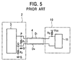
- Fig. 5 is a block circuit diagram illustrating the connecting state between a conventional USB-compatible peripheral device (terminal) 10 and a host (computer unit) 2.
- a conventional USB-compatible peripheral device terminal
- a host computer unit
- Various types of devices such as a keyboard, a mouse, a printer, a speaker, a game controller, etc., may be used as the peripheral device 10 to be connected to the host 2 via a USB.
- the USB is formed of four lines, such as a pair of data lines (D+ line and D- line), a power line (Vcc), and a ground line (G).
- a USB port 3 is provided in the host 2, and a USB controller 11 is provided in the peripheral device 10.
- the USB controller 11 is connected to the USB port 3 via a USB-compatible cable 4.
- the data line D- line of the USB port 3 is connected to one end of a pull-down resistor R 1 , while the data line D+ line of the USB port 3 is connected to one end of a pull-down resistor R 2 .
- the other ends of the pull-down resistors R 1 and R 2 are connected to ground lines G.
- one end of a pull-up resistor R 3 is connected to the D- line and the other end is connected to the power line (Vcc).
- the potential at a point P in Fig. 5 is 0 volts (low state).
- the D- line, the D+ line, the power line Vcc, and a ground line of the peripheral device 10 are connected to the counterparts of the host 2, and the potential at the point P is increased (high state).
- the host 2 identifies such a potential increase, it is determined that the peripheral device 10 is connected to the host 2.
- the host 2 starts to perform a polling operation by calling the peripheral device 10 at regular intervals so that mutual communications are established between the host 2 and the peripheral device 10.
- the peripheral device 10 upon receiving a calling signal from the host 2, the peripheral device 10 returns a signal to the host 2 in response to the calling signal regardless of whether the peripheral device 10 is operated.
- the point P When the cable 4 is disconnected to remove the peripheral device 10 from the host 2, the point P is connected to the ground line G and decreases to 0 volts. A potential drop is detected in the host 2, and thus, the host 2 determines that the peripheral device 10 is disconnected.
- the host 2 is able to determine whether the peripheral device 10 is connected or disconnected.
- the host 2 discontinues the polling to the peripheral device 10, thereby interrupting the communications between the host 2 and the peripheral device 10.
- the cable 4 of the peripheral device 10 must first be disconnected from the USB port 3 so that the potential at the point P drops to a ground potential (low state), and the cable 4 must then be re-inserted into the USB port 3 so that the potential is again raised to the high state. Alternatively, an operating system loaded in the host 2 must be restarted.
- the peripheral device 10 possesses a resetting (initializing) function.
- a malfunction occurs in the peripheral device 10, such as a voltage change, the departure of processing from a fixed program routine, or a memory malfunction
- the peripheral device 10 automatically detects such a malfunction and performs a resetting operation. If there is no answer from the peripheral device 10 in response to the polling by the host 2 a predetermined number of times and communications therebetween are interrupted during the occurrence of the above-described malfunction, the peripheral device 10 accordingly performs the resetting operation to recover itself.
- connection unit for a peripheral device which automatically recovers interrupted communications between the peripheral device and a host without the need for a user to restart a system or remove and insert a cable.
- connection unit for a peripheral device which is connected to a host via a data line.
- the data line is set at a predetermined potential (high state) when communications are performed between the peripheral device and the host.
- the connection unit includes a recovering unit for establishing an apparently reconnected state between the peripheral device and the host by decreasing the potential of the data line (low state) from the predetermined potential when the communications between the peripheral device and the host are disabled and then by increasing the potential of the data line (high state) to the predetermined potential.
- the aforementioned recovering unit even if communications between the peripheral device and the host (polling from the host to the peripheral device) are interrupted, they can be apparently reconnected without the need for physically disconnecting them, thereby automatically recovering the normal communication state. This eliminates the need for the operator to remove and reinsert a cable between the peripheral device and the host or to restart the system.
- the data line may be connected to a ground via a first resistor in the host and may be connected to a power supply via a second resistor in the peripheral device.
- the recovering unit may establish the apparently reconnected state between the peripheral device and the host by setting the data line to the low state in the peripheral device and then by resetting the data line to the high state.
- the data line may include a D- line and a D+ line
- the recovering unit may establish the apparently reconnected state between the peripheral device and the host by setting at least one of the D- line and the D+ line to the low state in the peripheral device and then by resetting the data line to the high state.
- a switch for controlling the current flow may be disposed as the recovering unit on at least one of the D- line or the D+ line of the peripheral device.
- the switch is controlled to apparently disconnect the D- line or the D+ line between the peripheral device and the host. This decreases the potential of the D- line or the D+ line provided with the second resistor to the ground potential, and the host determines that the peripheral device is disconnected though it is not physically removed.
- the peripheral device then resets the switch to the state before the data line is apparently disconnected, thereby increasing the potential of the D- line or the D+ line.
- the host determines that the peripheral device is reconnected.
- the recovering unit may establish the apparently reconnected state between the peripheral device and the host by connecting the data line to a ground or causing a portion between the data line and the power supply to become a high impedance to set the portion to the low state and then resetting the portion to the high state.
- the data line in setting the data line to the low state, may be directly grounded, or the second resistor between the data line and the power supply may be grounded.
- the data line may be temporarily opened, or the portion between the second resistor and the power supply may be opened, thereby causing it to become a high impedance. In this case, advantages similar to those exhibited by the above case may be obtained.
- the host may regularly call the peripheral device via the data line, and the recovering unit may establish the apparently reconnected state between the peripheral device and the host when there is no answer from the peripheral device in response to calling by the host a predetermined number of consecutive times.
- the recovering unit the aforementioned predetermined number of consecutive times of calling is determined by the specifications, and the recovering unit is operated when the peripheral device determines that the host is not calling.
- the recovering unit may establish the apparently reconnected state between the peripheral device and the host when detecting that one of the cases of a voltage change, departure of processing from a fixed program routine, and a memory malfunction occurs in the peripheral device.
- the recovering unit may be operated not only when one of the above-described malfunction occurs in the peripheral device, but also when the calling to the peripheral device is interrupted due to a malfunction occurring in the host.
- a personal computer is provided as a host, while a device (such as a keyboard or a mouse) loaded with a USB interface is provided as a peripheral device.
- FIG. 1A a connecting unit for a peripheral device according to a first embodiment of the present invention is shown.
- a peripheral device 1 shown in Fig. 1A has a built-in USB controller 5 which is provided with a pair of data lines (D+ line and D-line).
- D+ line and D-line data lines
- communications are performed by using a pair of signal lines (D+ line and D- line), and a positive potential and a negative potential, which are inverted with each other, are supplied to the two signal lines (D+ line and D- line), respectively.
- a second resistor R 3 (hereinafter referred to as the pull-up resistor R 3 ) Is connected at one end to the D- line within the peripheral device 1.
- the other end of the pull-up resistor R 3 is connected to a power line (Vcc).
- a change-over switch 6 is also provided for the D- line.
- a control unit 5a is disposed within the USB controller 5 so as to control the change-over switch 6 to be on or off via a control line 7.
- the change-over switch 6 is normally closed.
- the D- line and the D+ line are connected to an interface circuit (not shown).
- a host 2 shown in Fig. 1A has a built-in USB port 3.
- the USB port 3 is provided with terminals formed of a pair of data lines (D+ line and D- line), a power line (not shown), and a ground line G.
- One end of a first resistor R 1 (hereinafter referred to as the pull-down resistor R 1 ) is connected to the D- line of the host 2, and the other end is connected to the ground line G.
- One end of another first resistor R 2 (hereinafter referred to as the pull-down resistor R 2 ) is connected to the D+ line of the host 2, and the other end is connected to the ground line G.
- the power line Vcc of the peripheral device 1 is connected to the power line of the host 2, so that the peripheral device 1 is able to receive power from the host 2.
- a ground line (not shown) of the peripheral device 1 is connected to the ground line G of the host 2.
- a point P of the D- line shown in Fig. 1A is substantially at the same potential as that of the ground line G (ground potential, i.e., substantially 0 volts) (low state).
- the D+ line and the D- line of the peripheral device 1 are connected to the counterparts of the host 2, and as a result, the potential at the point P of the D- line is raised to a predetermined voltage (high state), which is different from the ground potential.
- USB-compatible peripheral devices operate in a high speed mode (12 Mbits/s) or a low speed mode (1.5 Mbits/s) according to the specifications. It is determined in which mode the peripheral device is operated according to the type of peripheral device. That is, in the low-speed-mode peripheral devices, a pull-up resistor is provided for the D- line, while in the high-speed-mode peripheral devices, a pull-up resistor is provided for the D+ line. Accordingly, when a low-speed-mode peripheral device is connected to the host 2, lines are formed by the power line Vcc, the pull-up resistor R 3 , the pull-down resistor R 1 , and the ground line G.
- the potential generated at the point P can be expressed by (R 1 /(R 1 + R 3 )) ⁇ I (see Figs. 1 and 2).
- lines are formed by the power line Vcc, a pull-up resistor R 4 , the pull-down resistor R 2 , and the ground line G.
- the potential generated at a point Q shown in Fig. 3 can be expressed by (R 2 /(R 2 + R 4 )) ⁇ I .
- the change-over switch 6 is controlled to be on or off by the control unit 5a disposed within the USB controller 5 via the control line 7.
- the change-over switch 6 may be formed by a regular transistor, such as a junction transistor of a field effect transistor (FET).
- FET field effect transistor
- the change-over switch 6 When a signal having a potential not greater than the predetermined potential (low signal) is input from the control unit 5a to the change-over switch 6 via the control line 7, the change-over switch 6 is closed. Conversely, the change-over switch 6 may be opened when a signal having a potential not greater than the predetermined potential is input, and may be closed when a signal having a potential exceeding the predetermined potential is input.
- the host 2 When the peripheral device 1 is connected, the host 2 performs a polling operation by calling the peripheral device 1 at regular intervals. If there is no answer in response to, for example, three consecutive calls, the host 2 discontinues the polling operation.
- the polling may be discontinued when malfunctions occur, such as a voltage increasing over a permissible level, the departure of processing from a fixed program routine, and a memory malfunction.
- the peripheral device 1 possesses a resetting (initializing) function. Upon detecting the above-described abnormality, the peripheral device 1 automatically performs the resetting operation. During the resetting operation, the polling operation is discontinued. If, however, the peripheral device 1 detects the occurrence of a malfunction and immediately resets itself while the host 2 is calling the peripheral device 1 three consecutive times, the polling may not be discontinued.
- the change-over switch 6 When the peripheral device 1 identifies the discontinuation of the polling, the change-over switch 6 is changed. As stated above, the change-over switch 6 is normally opened, and when a signal having a potential exceeding the predetermined potential is input from the control unit 5a via the control line 7, the circuit of the change-over switch 6 is opened. Accordingly, the D- line becomes a high impedance, and the potential at the point P is fixed at a potential substantially equal to the ground line G (ground potential) (low state). As a result, the host 2 detects the low potential of the point P and determines that the peripheral device 1 is disconnected from the host 2.
- a signal having a potential not greater than the predetermined potential is input from the control unit 5a to the change-over switch 6 via the control line 7, whereby the circuit of the change-over switch 6 is closed. Then, the potential at the point P is fixed at, for example, a predetermined power supply voltage (high state), and the host 2 identifies that the peripheral device 1 is connected.
- the host 2 and the peripheral device 1 are apparently re-connected so that the polling operation can be restarted, thereby enabling the peripheral device 1 to send data.
- FIG. 1B A peripheral device 1' constructed in accordance with a second embodiment of the present invention is shown In Fig. 1B.
- the change-over switch 6, which is disposed outside the USB controller 5 in Fig. 1A, is provided within the USB controller 5.
- the D-line and the D+ line are connected to an interface circuit 5b, and the change-over switch 6 is controlled to be on or off by the control unit 5a via the control line 7.
- the D-line and the D+ line may be located opposite to those discussed above.
- the D- line (or D+ line) is changed to a high impedance and is thus set in the low state.
- the change-over switch 6 is changed from the low state to the high state in a manner similar to the switching operation discussed above.
- a peripheral device 20 constructed in accordance with a third embodiment of the present invention is shown in Fig. 2A.
- the peripheral device 20 is provided with a line 8 on the D- line which is connected to a ground line G3 (which is to be connected to the ground line G of the host 2), and a change-over switch 26 is disposed in the line 8.
- the change-over switch 26, as in the change-over switch 6, is formed of a regular transistor, and is controlled by a control unit 25a disposed within a USB controller 25 via a control line 27. It should be noted that the change-over switch 26 is opened in the normal state.
- the portions other than the above-described elements are similar to those of the first embodiment shown in Fig. 1A and are designated by like reference numerals. An explanation thereof will thus be omitted.
- the circuit of the change-over switch 26 is closed by the control unit 25a via the control line 27. That is, a signal having a potential not greater than a predetermined potential is input from the control unit 25a, and the change-over switch 26 is closed. Accordingly, the power supplied from the power line Vcc entirely flows into the ground line G3 via the line 8 rather than flowing into the host 2.
- the potential at the point P is set to be substantially the ground potential of the ground line G (low state), and the host 2 determines that the peripheral device 20 is disconnected.
- a signal having a potential exceeding the predetermined potential is supplied from the control unit 25a to the change-over switch 26 via the control line 27, thereby opening the change-over switch 26.
- the potential at the point P on the D- line is raised to a predetermined power supply voltage (high state), and the host 2 determines that the peripheral device 20 is connected.
- a circuit consisting of the ground line G3 and the change-over switch 26 may be formed within the USB controller 25, and the change-over switch 26 may be controlled by the control unit 25a.
- a peripheral device 20' constructed in accordance with a fourth embodiment of the present invention is shown in Fig. 2B.
- the change-over switch 26, the pull-up resistor R 3 , and the power line Vcc which are disposed outside the USB controller 25 in Fig. 2A, are disposed within the USB controller 25.
- the D-line and the D+ line are connected to an interface circuit 25b, and the change-over switch 26 is controlled to be on or off by the control unit 25a via the control line 27.
- the D-line and the D+ line may be located opposite to those discussed above.
- the change-over switch 26 is closed so that the D- line (or D+ line) is connected to the ground and is set in the low state.
- Fig. 3 illustrates a high-speed-mode peripheral device 30 constructed in accordance with a fifth embodiment of the present invention.
- one end of the pull-up resistor R 4 is connected to the D+ line, and the other end is connected to the power line Vcc.
- a change-over switch 36 is provided for the D+ line of the peripheral device 30, and is controlled to be on or off by a control unit 35a disposed within a USB controller 35 via a control line 37. In the normal state, the change-over switch 36 is closed. When it is determined that the polling operation is not performed by the host 2, the circuit of the change-over switch 36 is opened, and is then closed.
- the D+ line is connected to the power line Vcc via the pull-up resistor R 4 .
- the potential at the point Q shown in Fig. 3 can be expressed by (R 2 /(R 2 + R 4 )) ⁇ I , and is increased from the ground potential (low state). By detecting this increased potential, the host 2 determines that the peripheral device 30 is connected to the host 2.
- the configuration of the peripheral device 30 is not restricted to the fifth embodiment shown in Fig. 3, and the change-over switch 36 may be disposed within the USB controller 35, as in the case of the peripheral device 1' shown In Fig. 1B, and may be controlled to be on or off by the control unit 35a via the control line 37.
- a circuit consisting of the change-over switch 36, the pull-up resistor R 4 , and the power line Vcc may be formed within the USB controller 35, as in the case of the peripheral device 20' shown in Fig. 2B, and the change-over switch 36 may be controlled to be on or off by the control unit 35a.
- Fig. 4 illustrates a peripheral device 40 constructed in accordance with a sixth embodiment of the present invention.
- a change-over switch 46 is provided between the power line Vcc and the pull-up resistor R 3 .
- the change-over switch 46 is opened to disconnect the power line Vcc and the pull-up resistor R 3 .
- the portion between the D- line (or D+ line) and the power line Vcc becomes a high impedance and is set in the low state.
- the pull-up resistor R 3 may be connected to the ground G, whereby the D- line (or D+ line) is set in the low state.
- the change-over switch 46 can be selectively changed among three states, as illustrated in Fig. 4: a connecting state between the power line Vcc and the pull-up resistor R 3 (state a), an open state between the power line Vcc and the pull-up resistor R 3 (state b), and a connecting state (state c) between the pull-up resistor R 3 and the ground line G.
- the change-over switch 46 When the change-over switch 46 is changed to the state b by a control unit 45a disposed within a USB controller 45 via a control line 47, the portion between the power line Vcc and the D- line (or D+ line) (data line) becomes a high impedance and is set in the low state. Then, when the change-over switch 46 is changed to the state c, the pull-up resistor R 3 is connected to the ground G so that the D- line is set at the ground potential and is thus set in the low state. Accordingly, the host 2 identifies that the peripheral device 40 is disconnected.
- change-over switch 46 it is not essential that the change-over switch 46 be changeable among the three states, and it may be changed between the state a and state b or between the state a and the state c.
- a circuit consisting of the pull-up resistor R 3 , the change-over switch 46, the power line Vcc, and the ground G may be formed within the USB controller 45.
- control units 5a, 25a, 35a, and 45a may be disposed outside the USB controllers 5, 25, 35, and 45, respectively, and control the change-over switches 6, 26, 36, and 46, respectively.
- the configuration of the present invention is not limited to the foregoing embodiments as long as the potential at the point P or the point Q on the data line can be switched between the high state and the low state.
- the D- line and the D+ line may be short-circuited, or the change-over switch may be provided for a host.
Landscapes
- Engineering & Computer Science (AREA)
- Theoretical Computer Science (AREA)
- Physics & Mathematics (AREA)
- General Engineering & Computer Science (AREA)
- General Physics & Mathematics (AREA)
- Information Transfer Systems (AREA)
- Power Sources (AREA)
- Input From Keyboards Or The Like (AREA)
- Remote Monitoring And Control Of Power-Distribution Networks (AREA)
- Direct Current Feeding And Distribution (AREA)
Abstract
Description
Claims (6)
- A connection unit for a peripheral device which is connected to a host via a data line, said data line being set at a predetermined potential (high state) when communications are performed between said peripheral device and said host, said connection unit comprising recovering means for establishing an apparently reconnected state between said peripheral device and said host by decreasing the potential of said data line (low state) from the predetermined potential when the communications between said peripheral device and said host are disabled and then by increasing the potential of said data line (high state) to the predetermined potential.
- A connection unit according to claim 1, wherein said data line is connected to a ground via a first resistor in said host and is connected to a power supply via a second resistor in said peripheral device, and said recovering means establishes the apparently reconnected state between said peripheral device and said host by setting said data line to the low state in said peripheral device and then by resetting said data line to the high state.
- A connecting unit according to claim 2, wherein said data line comprises a D- line and a D+ line, and said recovering means establishes the apparently reconnected state between said peripheral device and said host by setting at least one of the D- line and the D+ line to the low state in said peripheral device and then by resetting said data line to the high state.
- A connecting unit according to claim 1, wherein said recovering means establishes the apparently reconnected state between said peripheral device and said host by performing one of connecting said data line to a ground and causing a portion between said data line and said power supply to become a high impedance to set the portion to the low state and then resetting the portion to the high state.
- A connecting unit according to claim 1, wherein said host regularly calls said peripheral device via said data line, and said recovering means establishes the apparently reconnected state between said peripheral device and said host when there is no answer from said peripheral device in response to calling by said host a predetermined number of consecutive times.
- A connecting unit according to claim 1, wherein said recovering means establishes the apparently reconnected state between said peripheral device and said host when detecting that one of the cases of a voltage change, departure of processing from a fixed program routine, and a memory malfunction occurs in said peripheral device.
Applications Claiming Priority (2)
| Application Number | Priority Date | Filing Date | Title |
|---|---|---|---|
| JP24852199 | 1999-09-02 | ||
| JP24852199A JP3795712B2 (en) | 1999-09-02 | 1999-09-02 | Peripheral device connection device |
Publications (2)
| Publication Number | Publication Date |
|---|---|
| EP1085422A2 true EP1085422A2 (en) | 2001-03-21 |
| EP1085422A3 EP1085422A3 (en) | 2004-09-29 |
Family
ID=17179432
Family Applications (1)
| Application Number | Title | Priority Date | Filing Date |
|---|---|---|---|
| EP00306120A Withdrawn EP1085422A3 (en) | 1999-09-02 | 2000-07-18 | Connection unit for peripheral devices |
Country Status (5)
| Country | Link |
|---|---|
| US (1) | US6647452B1 (en) |
| EP (1) | EP1085422A3 (en) |
| JP (1) | JP3795712B2 (en) |
| CN (1) | CN1127024C (en) |
| TW (1) | TW511032B (en) |
Cited By (13)
| Publication number | Priority date | Publication date | Assignee | Title |
|---|---|---|---|---|
| WO2003071438A1 (en) * | 2002-02-19 | 2003-08-28 | Infineon Technologies Ag | A method for a first semiconductor device to determine if it is coupled to a second semiconductor device |
| US6936841B2 (en) | 2001-06-01 | 2005-08-30 | D-Wave Systems, Inc. | Methods for controlling qubits |
| EP1967948A2 (en) * | 2007-03-08 | 2008-09-10 | Samsung Electronics Co., Ltd. | Image display apparatus for controlling an external data transmitting device using a USB connector and a method thereof |
| EP2687993A1 (en) * | 2012-07-16 | 2014-01-22 | VeriFone, Inc. | USB apparatus and embedded system incorporating same |
| EP2947575A3 (en) * | 2014-05-23 | 2015-12-09 | Kyocera Document Solutions Inc. | Electronic device and method for switching between a normal power mode and a power saving mode of an electronic device |
| CN114297122A (en) * | 2021-12-27 | 2022-04-08 | 杭州海康威视数字技术股份有限公司 | Universal Serial Bus (USB) interface circuit and electronic equipment |
| US11790259B2 (en) | 2019-09-06 | 2023-10-17 | D-Wave Systems Inc. | Systems and methods for tuning capacitance in quantum devices |
| US12224750B2 (en) | 2021-09-03 | 2025-02-11 | 1372934 B.C. Ltd. | Topologically protected qubits, processors with topologically protected qubits, and methods for use of topologically protected qubits |
| US12301225B2 (en) | 2021-07-23 | 2025-05-13 | 1372934 B.C. Ltd. | Systems and methods for tuning capacitance in quantum devices |
| US12475399B2 (en) | 2021-12-14 | 2025-11-18 | D-Wave Systems Inc. | Systems and methods for increasing energy-scale by minimizing qubit inductance |
| US12519471B2 (en) | 2021-12-17 | 2026-01-06 | 1372934 B.C. Ltd. | Systems and methods for qubit control |
| US12626176B2 (en) | 2020-03-27 | 2026-05-12 | D-Wave Systems Inc. | Systems and methods for scalable quantum computing |
| US12632760B2 (en) | 2020-12-15 | 2026-05-19 | D-Wave Systems Inc. | Systems and methods for tuning capacitance of qubits |
Families Citing this family (36)
| Publication number | Priority date | Publication date | Assignee | Title |
|---|---|---|---|---|
| US20020083430A1 (en) * | 2000-12-26 | 2002-06-27 | Tadao Kusuda | Uninstall control apparatus which controls uninstallation of device control software |
| US7370239B2 (en) * | 2001-05-31 | 2008-05-06 | Fisher-Rosemount Systems, Inc. | Input/output device with configuration, fault isolation and redundant fault assist functionality |
| KR100421050B1 (en) * | 2001-10-12 | 2004-03-04 | 삼성전자주식회사 | Universal serial bus device having logical circuit for conversive and immediate USB Host reset operation |
| JP2003158561A (en) * | 2001-11-21 | 2003-05-30 | Nec Corp | Mobile phone |
| AU2003281098A1 (en) * | 2002-07-15 | 2004-02-02 | Axalto Sa | Usb device |
| US6738834B1 (en) * | 2002-07-15 | 2004-05-18 | Cypress Microsystems | System for reconfiguring a peripheral device using configuration residing on the peripheral device by electronically simulating a physical disconnection and reconnection to a host device |
| US7260749B2 (en) * | 2003-01-22 | 2007-08-21 | Red Hat, Inc. | Hot plug interfaces and failure handling |
| JP2005079722A (en) * | 2003-08-28 | 2005-03-24 | Kyocera Corp | Information equipment |
| JP4601330B2 (en) * | 2004-05-25 | 2010-12-22 | ソニー株式会社 | Electronic device and control method thereof, information processing apparatus, and computer program |
| DE102004031278B4 (en) * | 2004-06-28 | 2008-06-12 | Infineon Technologies Ag | Device for detecting the connection of peripheral devices to a host system |
| CN100357921C (en) * | 2004-12-31 | 2007-12-26 | 联想(北京)有限公司 | Method for controlling automatic running program in USB memory and USB memory thereof |
| KR100765267B1 (en) * | 2005-06-29 | 2007-10-09 | 삼성전자주식회사 | Electronic device and its control method and electronic control system including the same |
| JP4973036B2 (en) * | 2005-08-08 | 2012-07-11 | セイコーエプソン株式会社 | Host controller |
| US8346981B2 (en) * | 2005-08-23 | 2013-01-01 | Mcci Corporation | Connection of peripherals to operating systems |
| CN100409149C (en) * | 2005-10-28 | 2008-08-06 | 环达电脑(上海)有限公司 | Connection channel device between PC machine and built-in equipment GPS module and communication method |
| US7698490B2 (en) * | 2005-12-21 | 2010-04-13 | Nvidia Corporation | Passive USB power configuration switching |
| JP4876236B2 (en) * | 2006-09-01 | 2012-02-15 | 日本電産サンキョー株式会社 | USB communication system, USB device, and abnormality detection method for USB communication system |
| JP4872553B2 (en) * | 2006-09-14 | 2012-02-08 | 大日本印刷株式会社 | Information processing apparatus and method for automatically recovering connection failure of USB device |
| JP2008152533A (en) * | 2006-12-18 | 2008-07-03 | Hitachi Omron Terminal Solutions Corp | USB device, USB connection system, USB device removal recognition simulation method, and USB device re-recognition method |
| US20080235524A1 (en) * | 2007-03-16 | 2008-09-25 | Sharma Yugal K | System for peripheral re-enumeration |
| US20090037622A1 (en) * | 2007-08-02 | 2009-02-05 | Broadcom Corporation | Method and system for changing operation modes of an interface device |
| US20090199044A1 (en) * | 2008-01-31 | 2009-08-06 | Hurrell Nicholas J | Device self-maintenance |
| US8020049B2 (en) * | 2008-12-18 | 2011-09-13 | Avago Technologies Ecbu Ip (Singapore) Pte. Ltd. | Detection of and recovery from an electrical fast transient/burst (EFT/B) on a universal serial bus (USB) device |
| CN101674366B (en) * | 2009-09-19 | 2012-03-28 | 惠州Tcl移动通信有限公司 | Mobile terminal USB, or charger inserting identification method and identification device thereof |
| US8631284B2 (en) | 2010-04-30 | 2014-01-14 | Western Digital Technologies, Inc. | Method for providing asynchronous event notification in systems |
| US8762682B1 (en) | 2010-07-02 | 2014-06-24 | Western Digital Technologies, Inc. | Data storage apparatus providing host full duplex operations using half duplex storage devices |
| US8996747B2 (en) | 2011-09-29 | 2015-03-31 | Cypress Semiconductor Corporation | Methods and physical computer-readable storage media for initiating re-enumeration of USB 3.0 compatible devices |
| US20130067119A1 (en) * | 2011-09-09 | 2013-03-14 | Chi Kwok Wong | Boot up configuration with usb data pins in embedded systems |
| US8843664B2 (en) | 2011-09-29 | 2014-09-23 | Cypress Semiconductor Corporation | Re-enumeration of USB 3.0 compatible devices |
| US9395799B2 (en) | 2012-08-09 | 2016-07-19 | Nvidia Corporation | Power management techniques for USB interfaces |
| CN102831084B (en) * | 2012-08-16 | 2015-07-22 | 刘伟 | Controller and controlling method for re-identifying USB (universal serial bus) equipment |
| US10282334B2 (en) | 2015-10-30 | 2019-05-07 | Response Technologies, Ltd. | Communication module for a security system and method for same |
| US10713205B2 (en) * | 2017-02-24 | 2020-07-14 | Digital 14 Llc | Universal serial bus (USB) disconnection switch system, computer program product, and method |
| JP6905134B1 (en) | 2020-09-07 | 2021-07-21 | 日本たばこ産業株式会社 | Power supply unit of aerosol generator |
| JP6856810B1 (en) * | 2020-09-07 | 2021-04-14 | 日本たばこ産業株式会社 | Power supply unit of aerosol generator |
| JP6856811B1 (en) | 2020-09-07 | 2021-04-14 | 日本たばこ産業株式会社 | Power supply unit of aerosol generator |
Family Cites Families (11)
| Publication number | Priority date | Publication date | Assignee | Title |
|---|---|---|---|---|
| US5761448A (en) | 1996-08-30 | 1998-06-02 | Ncr Corporation | Physical-to-logical bus mapping scheme for computer systems having multiple PCI bus configuration |
| US6073193A (en) * | 1997-04-24 | 2000-06-06 | Cypress Semiconductor Corp. | Fail safe method and apparatus for a USB device |
| US6012103A (en) * | 1997-07-02 | 2000-01-04 | Cypress Semiconductor Corp. | Bus interface system and method |
| US5974486A (en) * | 1997-08-12 | 1999-10-26 | Atmel Corporation | Universal serial bus device controller comprising a FIFO associated with a plurality of endpoints and a memory for storing an identifier of a current endpoint |
| JPH11194993A (en) * | 1998-01-06 | 1999-07-21 | Alps Electric Co Ltd | Usb controller |
| JPH11194847A (en) * | 1998-01-06 | 1999-07-21 | Toshiba Corp | Computer system and initialization controller |
| JP4045009B2 (en) * | 1998-04-02 | 2008-02-13 | セイコーエプソン株式会社 | USB controller and device equipped with the same |
| TW444165B (en) * | 1998-05-12 | 2001-07-01 | Primax Electronics Ltd | Hot plug and play universal serial bus switch device and control method |
| TW410516B (en) * | 1998-07-28 | 2000-11-01 | Novatek Microelectronics Corp | Electromagnetic safety enhancement device for universal serial bus and method thereof |
| US6279060B1 (en) * | 1998-12-04 | 2001-08-21 | In-System Design, Inc. | Universal serial bus peripheral bridge simulates a device disconnect condition to a host when the device is in a not-ready condition to avoid wasting bus resources |
| US6415342B1 (en) * | 1999-07-27 | 2002-07-02 | Hewlett-Packard Company | Universal serial bus controlled connect and disconnect |
-
1999
- 1999-09-02 JP JP24852199A patent/JP3795712B2/en not_active Expired - Fee Related
-
2000
- 2000-07-18 EP EP00306120A patent/EP1085422A3/en not_active Withdrawn
- 2000-08-02 TW TW089115528A patent/TW511032B/en not_active IP Right Cessation
- 2000-08-29 CN CN00124433.7A patent/CN1127024C/en not_active Expired - Fee Related
- 2000-08-30 US US09/650,941 patent/US6647452B1/en not_active Expired - Fee Related
Cited By (15)
| Publication number | Priority date | Publication date | Assignee | Title |
|---|---|---|---|---|
| US6936841B2 (en) | 2001-06-01 | 2005-08-30 | D-Wave Systems, Inc. | Methods for controlling qubits |
| WO2003071438A1 (en) * | 2002-02-19 | 2003-08-28 | Infineon Technologies Ag | A method for a first semiconductor device to determine if it is coupled to a second semiconductor device |
| EP1967948A2 (en) * | 2007-03-08 | 2008-09-10 | Samsung Electronics Co., Ltd. | Image display apparatus for controlling an external data transmitting device using a USB connector and a method thereof |
| EP2687993A1 (en) * | 2012-07-16 | 2014-01-22 | VeriFone, Inc. | USB apparatus and embedded system incorporating same |
| US8850097B2 (en) | 2012-07-16 | 2014-09-30 | Verifone, Inc. | USB apparatus and embedded system incorporating same |
| EP2947575A3 (en) * | 2014-05-23 | 2015-12-09 | Kyocera Document Solutions Inc. | Electronic device and method for switching between a normal power mode and a power saving mode of an electronic device |
| US11790259B2 (en) | 2019-09-06 | 2023-10-17 | D-Wave Systems Inc. | Systems and methods for tuning capacitance in quantum devices |
| US12099901B2 (en) | 2019-09-06 | 2024-09-24 | D-Wave Systems Inc. | Systems and methods for tuning capacitance in quantum devices |
| US12626176B2 (en) | 2020-03-27 | 2026-05-12 | D-Wave Systems Inc. | Systems and methods for scalable quantum computing |
| US12632760B2 (en) | 2020-12-15 | 2026-05-19 | D-Wave Systems Inc. | Systems and methods for tuning capacitance of qubits |
| US12301225B2 (en) | 2021-07-23 | 2025-05-13 | 1372934 B.C. Ltd. | Systems and methods for tuning capacitance in quantum devices |
| US12224750B2 (en) | 2021-09-03 | 2025-02-11 | 1372934 B.C. Ltd. | Topologically protected qubits, processors with topologically protected qubits, and methods for use of topologically protected qubits |
| US12475399B2 (en) | 2021-12-14 | 2025-11-18 | D-Wave Systems Inc. | Systems and methods for increasing energy-scale by minimizing qubit inductance |
| US12519471B2 (en) | 2021-12-17 | 2026-01-06 | 1372934 B.C. Ltd. | Systems and methods for qubit control |
| CN114297122A (en) * | 2021-12-27 | 2022-04-08 | 杭州海康威视数字技术股份有限公司 | Universal Serial Bus (USB) interface circuit and electronic equipment |
Also Published As
| Publication number | Publication date |
|---|---|
| US6647452B1 (en) | 2003-11-11 |
| TW511032B (en) | 2002-11-21 |
| JP3795712B2 (en) | 2006-07-12 |
| CN1127024C (en) | 2003-11-05 |
| CN1287313A (en) | 2001-03-14 |
| EP1085422A3 (en) | 2004-09-29 |
| JP2001075713A (en) | 2001-03-23 |
Similar Documents
| Publication | Publication Date | Title |
|---|---|---|
| US6647452B1 (en) | Automatic recovery of non-responsive peripheral device by apparent disconnect and reconnect | |
| JP4961999B2 (en) | Electronics | |
| US5802328A (en) | Apparatus for detecting correct insertion of a PC card in an information processing system | |
| JP3610424B2 (en) | Electronic equipment and interface circuit | |
| US6920569B1 (en) | Device configured as stand-alone or slave based on detection of power supply in a powered data bus system | |
| US5848292A (en) | System for data transmission between a wedge microcontroller and a personal computer microcontroller by disconnecting the keyboard microcontroller and placing the same in hold state | |
| US6633935B1 (en) | Automatic bus termination readjustment | |
| JP2000316006A (en) | Node having provision for bus manager function automatic changeover, mobile terminal and mobile terminal system | |
| EP2625620B1 (en) | Remote access appliance with communication protocol autosensing feature | |
| CN1493138B (en) | communication device | |
| US5297141A (en) | Ethernet automatic adapter interface card | |
| JP3186938B2 (en) | External power on / off control system | |
| KR20010015076A (en) | Signal input and output apparatus | |
| US5258655A (en) | Apparatus for electrically switching between peripheral devices | |
| CN101170780B (en) | Method for dual mode terminal to prevent from current backflow between two radio modules | |
| EP1152320A1 (en) | Power switch circuit and electronic device | |
| US20040027006A1 (en) | Power supply switch circuit and electronic device | |
| JP2001042975A (en) | Information processor | |
| EP1181837B1 (en) | Ieee 1394 cable connector with short circuit switch | |
| CN220307228U (en) | Gateway (GW) | |
| JP2821358B2 (en) | Tabletop | |
| JP2006018659A (en) | Electronic device and method for switching operation mode of electronic device | |
| JP2003114745A (en) | Usb controller | |
| KR20010019356A (en) | Apparatus and method processing malfunction by electro static discharge in universal serial bus device | |
| JP3031099B2 (en) | Portable printer |
Legal Events
| Date | Code | Title | Description |
|---|---|---|---|
| PUAI | Public reference made under article 153(3) epc to a published international application that has entered the european phase |
Free format text: ORIGINAL CODE: 0009012 |
|
| AK | Designated contracting states |
Kind code of ref document: A2 Designated state(s): AT BE CH CY DE DK ES FI FR GB GR IE IT LI LU MC NL PT SE |
|
| AX | Request for extension of the european patent |
Free format text: AL;LT;LV;MK;RO;SI |
|
| PUAL | Search report despatched |
Free format text: ORIGINAL CODE: 0009013 |
|
| AK | Designated contracting states |
Kind code of ref document: A3 Designated state(s): AT BE CH CY DE DK ES FI FR GB GR IE IT LI LU MC NL PT SE |
|
| AX | Request for extension of the european patent |
Extension state: AL LT LV MK RO SI |
|
| 17P | Request for examination filed |
Effective date: 20041211 |
|
| 17Q | First examination report despatched |
Effective date: 20050118 |
|
| AKX | Designation fees paid |
Designated state(s): DE FR GB |
|
| STAA | Information on the status of an ep patent application or granted ep patent |
Free format text: STATUS: THE APPLICATION HAS BEEN WITHDRAWN |
|
| 18W | Application withdrawn |
Effective date: 20060331 |