EP1085393A2 - Signal processing device - Google Patents
Signal processing device Download PDFInfo
- Publication number
- EP1085393A2 EP1085393A2 EP00119470A EP00119470A EP1085393A2 EP 1085393 A2 EP1085393 A2 EP 1085393A2 EP 00119470 A EP00119470 A EP 00119470A EP 00119470 A EP00119470 A EP 00119470A EP 1085393 A2 EP1085393 A2 EP 1085393A2
- Authority
- EP
- European Patent Office
- Prior art keywords
- reading
- clock signal
- signal
- halts
- maintained
- Prior art date
- Legal status (The legal status is an assumption and is not a legal conclusion. Google has not performed a legal analysis and makes no representation as to the accuracy of the status listed.)
- Withdrawn
Links
Images


Classifications
-
- G—PHYSICS
- G06—COMPUTING OR CALCULATING; COUNTING
- G06F—ELECTRIC DIGITAL DATA PROCESSING
- G06F21/00—Security arrangements for protecting computers, components thereof, programs or data against unauthorised activity
- G06F21/70—Protecting specific internal or peripheral components, in which the protection of a component leads to protection of the entire computer
- G06F21/71—Protecting specific internal or peripheral components, in which the protection of a component leads to protection of the entire computer to assure secure computing or processing of information
- G06F21/77—Protecting specific internal or peripheral components, in which the protection of a component leads to protection of the entire computer to assure secure computing or processing of information in smart cards
-
- G—PHYSICS
- G06—COMPUTING OR CALCULATING; COUNTING
- G06F—ELECTRIC DIGITAL DATA PROCESSING
- G06F21/00—Security arrangements for protecting computers, components thereof, programs or data against unauthorised activity
- G06F21/70—Protecting specific internal or peripheral components, in which the protection of a component leads to protection of the entire computer
- G06F21/71—Protecting specific internal or peripheral components, in which the protection of a component leads to protection of the entire computer to assure secure computing or processing of information
- G06F21/75—Protecting specific internal or peripheral components, in which the protection of a component leads to protection of the entire computer to assure secure computing or processing of information by inhibiting the analysis of circuitry or operation
- G06F21/755—Protecting specific internal or peripheral components, in which the protection of a component leads to protection of the entire computer to assure secure computing or processing of information by inhibiting the analysis of circuitry or operation with measures against power attack
-
- G—PHYSICS
- G06—COMPUTING OR CALCULATING; COUNTING
- G06F—ELECTRIC DIGITAL DATA PROCESSING
- G06F9/00—Arrangements for program control, e.g. control units
- G06F9/06—Arrangements for program control, e.g. control units using stored programs, i.e. using an internal store of processing equipment to receive or retain programs
- G06F9/30—Arrangements for executing machine instructions, e.g. instruction decode
- G06F9/38—Concurrent instruction execution, e.g. pipeline or look ahead
- G06F9/3867—Concurrent instruction execution, e.g. pipeline or look ahead using instruction pipelines
- G06F9/3869—Implementation aspects, e.g. pipeline latches; pipeline synchronisation and clocking
-
- G—PHYSICS
- G06—COMPUTING OR CALCULATING; COUNTING
- G06K—GRAPHICAL DATA READING; PRESENTATION OF DATA; RECORD CARRIERS; HANDLING RECORD CARRIERS
- G06K19/00—Record carriers for use with machines and with at least a part designed to carry digital markings
- G06K19/06—Record carriers for use with machines and with at least a part designed to carry digital markings characterised by the kind of the digital marking, e.g. shape, nature, code
- G06K19/067—Record carriers with conductive marks, printed circuits or semiconductor circuit elements, e.g. credit or identity cards also with resonating or responding marks without active components
- G06K19/07—Record carriers with conductive marks, printed circuits or semiconductor circuit elements, e.g. credit or identity cards also with resonating or responding marks without active components with integrated circuit chips
- G06K19/073—Special arrangements for circuits, e.g. for protecting identification code in memory
-
- G—PHYSICS
- G06—COMPUTING OR CALCULATING; COUNTING
- G06K—GRAPHICAL DATA READING; PRESENTATION OF DATA; RECORD CARRIERS; HANDLING RECORD CARRIERS
- G06K19/00—Record carriers for use with machines and with at least a part designed to carry digital markings
- G06K19/06—Record carriers for use with machines and with at least a part designed to carry digital markings characterised by the kind of the digital marking, e.g. shape, nature, code
- G06K19/067—Record carriers with conductive marks, printed circuits or semiconductor circuit elements, e.g. credit or identity cards also with resonating or responding marks without active components
- G06K19/07—Record carriers with conductive marks, printed circuits or semiconductor circuit elements, e.g. credit or identity cards also with resonating or responding marks without active components with integrated circuit chips
- G06K19/073—Special arrangements for circuits, e.g. for protecting identification code in memory
- G06K19/07309—Means for preventing undesired reading or writing from or onto record carriers
- G06K19/07363—Means for preventing undesired reading or writing from or onto record carriers by preventing analysis of the circuit, e.g. dynamic or static power analysis or current analysis
-
- G—PHYSICS
- G06—COMPUTING OR CALCULATING; COUNTING
- G06F—ELECTRIC DIGITAL DATA PROCESSING
- G06F2207/00—Indexing scheme relating to methods or arrangements for processing data by operating upon the order or content of the data handled
- G06F2207/72—Indexing scheme relating to groups G06F7/72 - G06F7/729
- G06F2207/7219—Countermeasures against side channel or fault attacks
Definitions
- the present invention is related to a signal processing device provided with a processor (CPU), a memory and so forth.
- the present invention is related to a signal processing device installed within a security equipment, an encryption device such as an IC card (smart card), an electronic lock and so forth.
- a security equipment such as an encryption device installed within an IC card (smart card), an electronic lock and so forth is provided generally with a signal processing device having a CPU, a memory and so forth for the verification of a password.
- the instruction execution cycle times as required for executing the respective instructions by means of the signal processing device are different from each other depending upon the execution types thereof. Accordingly, a respective instruction is executed at a predetermined time point after the signal processing device initiates instruction processing so that it is possible to analyze the operation of the signal processing device relating to the timing of the execution of a particular instruction, for example, by monitoring the time elapsed just after initiating a certain stage of the instruction processing triggered by resetting the internal CPU or receiving an external signal.
- pseudo routines which are useless and harmless, are inserted into the program routine executed by the signal processing device, as means for introducing irregularity to the sequence of instructions as executed in order to deceive the analysis of the operation of the signal processing device.
- the program routine including the pseudo routine may be executed in order to run the pseudo routine between the main routine for verifying a password and the internal phenomenon which is externally observable.
- the pseudo routine is repeated between the main routine and the internal phenomenon for a variable number of times, i.e., the frequency of repetition is determined at random for each appearance of the program routine.
- the present invention has been made in order to solve the shortcomings as described above. It is an object of the present invention therefore to provide a signal processing device with an improved reliability and an enhanced impenetrability against encryption analysis while avoiding substantial overhead on the processing time of the signal processing device.
- a wait signal is transmitted from a random signal generation circuit to the processor in a non-periodic manner in order to halt the processor at random.
- the operation state of the processor is maintained when haled, and the halted operation is continued from the operation state as maintained when resumed.
- the operation of the processor can be halted in a non-periodic manner, it is possible to prevent the operation of the processor from being analyzed by observing the internal phenomena of the processor.
- substantial overhead on the processing time of the signal processing device can be avoided by providing a short halting time period
- the clock signal as inputted to the processor can be deferred in a non-periodic manner.
- the modification it is possible to make more implicated patterns of the operation of the processor by the combination of deferring the clock signal in a non-periodic manner and the wait signal as output from the random signal generation circuit also in a non-periodic manner. As a result, the analysis of the operation of the signal processing device becomes furthermore difficult.
- the processor receives a password as said signal and matches the password against secret data stored in a memory in order to verify whether or not the password is in agreement with the secret data.
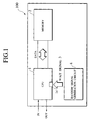
- Fig. 1 is a block diagram showing the configuration of the signal processing device 100 in accordance with the first embodiment of the present invention.
- the signal processing device 100 is composed of a CPU 1 for executing instruction sequences for such as a routine of verifying a password, a memory 2 for storing secret data such as the password and so forth, a random signal generation circuit 4 for generating a wait signal 3 which is output in order to halt the operation of the CPU 1.
- the CPU 1 is for example a semiconductor integrated circuit for taking control of the entirety of the signal processing device 100.
- the signal is interpretted and is matched against the secret data stored in the memory 2 by means of the CPU 1 in order to verify whether or not the password is in agreement with the secret data and output the verification result to an external device.
- the CPU 1 is provided with a wait signal input terminal 1a for receiving the wait signal 3.
- the CPU 1 halts its operation for a short time such as one to several clocks.
- the random signal generation circuit 4 is located beside the CPU 1.
- the random signal generation circuit 4 is composed of an integrated circuit such as an semiconductor device in order to output the wait signal 3 in a non-periodic manner.
- a signal such as a password is input to the CPU 1, which serves to process the signal in order to verify the signal by comparing it to the secret data stored in the memory 2.
- the wait signal is inputted to the CPU 1 from the random signal generation circuit 4 with random intervals during processing the signal.
- the CPU 1 then halts its operation for a certain period, for example, for one to several clocks.
- the CPU 1 maintains its operation state during the halting period. After resuming the operation, the CPU 1 continues the process handled just before it halts.
- the verification result is output from the CPU 1.
- the security of the signal processing device 100 is enhanced by making use of the waiting function provided for the CPU 1. Namely, in the case of the signal processing device 100, it takes a different number of clocks for a different time of initiating a certain routine to execute a particular instruction, and therefore making it difficult to analyze the operation of the CPU 1 and improving the security of the signal processing device 100. Particularly, since the random signal generation circuit 4 in accordance with this embodiment is capable of deferring the operation of the CPU 1 only for a short time such as for one to several clocks and therefore it is no longer the case that the progress of the task of the CPU 1 is substantially delayed.
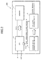
- Fig.2 is a block diagram showing the configuration of a signal processing device 200 in accordance with the second embodiment of the present invention.
- the first embodiment of the present invention has been described with the CPU of the signal processing device which is designed to halt the operation in response to the wait signal.
- the second embodiment is applicable to a signal processing device equipped with a CPU which is not provided with such a function.
- the signal processing device 200 is composed generally of a CPU 11 for executing instruction sequences for such as a routine of verifying a password, a memory 2 for storing secret data such as the password and so forth, a CPU clock control circuit 5 for controlling the supply of clock signals to the CPU 11, a random signal generation circuit 4 for generating a random signal 3 in order to control the operation of the CPU clock control circuit 5.
- the CPU 11 is not provided with the halt function responsive to the wait signal unlike the CPU 1 of the first embodiment.
- the CPU 11 is provided with a CPU operating clock signal input terminal 11a through which CPU operating clock signal 6 is inputted to the CPU 11.
- the CPU 11 is controllably operated with the CPU operating clock signal 6 as input from the CPU operating clock signal input terminal 11a.
- the CPU clock control circuit 5 serves to control the supply of the CPU operating clock signal the CPU 11. Namely, the CPU clock control circuit 5 serves to intercept the clock signal 7 to be supplied to the CPU 11 and transfer the clock signal 7 to the clock signal input terminal 11a of the CPU 11 as the CPU operating clock signal 6 under the control of the random signal from the random signal generation circuit 4.
- the random signal generation circuit 4 serves to supply the wait signal 3 to the CPU clock control circuit 5 in a non-periodic manner.
- the random signal generation circuit 4 serves to make irregular the frequency of the CPU operating clock signal 6 as outputted from the CPU clock control circuit 5 by inputting the wait signal to the CPU clock control circuit 5 in a random timing.
- a signal indicative of a password and the like is input to the CPU 11, which serves to process the signal in order to verify the signal by comparing it to the secret data stored in the memory 2.
- the wait signal is inputted to the CPU 11 from the random signal generation circuit 4 with random intervals in order to defer the CPU operating clock signal 6 in a non-periodic manner during processing the signal.
- the CPU 11 then halts its operation when deferring the supply of the CPU operating clock signal 6.
- the CPU 11 maintains its operation state having been taken just before it halts.
- the CPU 11 After resuming the supply of the CPU operating clock signal 6, the CPU 11 resumes and continues the halted task from the operation state having been maintained just before it halts.
- the irregular delay intermittently takes place during signal processing for handling a password by the signal processing device.
- the timing of the execution of a particular instruction can be modified at random for each running of the program routine. For this reason, it becomes difficult to analyze the operation of the CPU 11 and improving the security of the signal processing device 200.
- the random signal generation circuit 4 in accordance with this embodiment is capable of deferring the operation of the CPU 11 only for a short time such as for one to several clocks and therefore it is no longer the case that the progress of the task of the signal processing device 200 is substantially delayed.
- Fig.3 is a view for explaining a third embodiment of the present invention.
- Fig.3(a) is a general overview of a security card 10 in accordance with the third embodiment.
- Fig.3(a) and Fig.3(b) are block diagrams showing the internal structure of an IC chip provided within the security card 10.
- Fig.3(d) is a general overview of a verification device 13 of the security card 10.
- Fig.3(e) and Fig.3(f) are block diagrams showing verification circuits each of which is embedded in the verification device 13.
- the security card 10 is provided for use in the verification of the ID of an individual person and so forth.
- the security card 10 is a card made of a plastic or the like and equipped with a built-in IC chip 12 as illustrated in Fig.3(a).
- the IC chip 12 is composed of a CPU 1 for executing instruction sequences for such as a routine of verifying secret data and a memory 2 in which the ID of the owner of the security card 10 and a random signal generation circuit 4 for generating a wait signal 3 with random intervals. Also, the CPU 1 is connected to connection terminals 13a and 13b for receiving external signals.
- the CPU 1 is an integrated circuit provided for taking control of the entirety of the IC chip 12.
- the CPU 1 is provided with a wait signal input terminal 1a for receiving the wait signal.
- the wait signal When the wait signal is input, the CPU 1 halts its operation for a short time such as one to several clocks.
- the random signal generation circuit 4 is composed of an integrated circuit such as an semiconductor device in order to output the wait signal 3 in a non-periodic manner.
- a command signal is input to the CPU 1 through the connection terminals 13a and 13b.
- the CPU 1 interprets the command signal and, if the command signal is valid, the ID stored in the memory 2 is transmitted to the verification device 33.
- the wait signal is inputted to the CPU 1 from the random signal generation circuit 4 with random intervals during processing the signal.
- the CPU 1 then halts its operation for a certain period, for example, for one to several clocks.
- the CPU 1 maintains its operation state during the halting period. After resuming the operation, the CPU 1 resumes and continues the halted task from the operation state having been maintained just before it halts. When the verification of the command signal is completed, the verification result is output from the CPU 1.
- the IC chip 12 can be replaced by an IC chip 12' which is modified as illustrated in Fig.3(c).
- the IC chip 12' is composed of a CPU 11 for executing instruction sequences for such as a routine for verification and the like, a memory 2 for storing an ID, a CPU clock control circuit 5 for controlling the supply of clock signals to the CPU 11, a random signal generation circuit 4 for generating a random signal 3 in order to control the operation of the CPU clock control circuit 5.
- the CPU 11 is not provided with the halt function responsive to the wait signal unlike the CPU 1 of the first embodiment.
- the CPU 11 is controllably operated with the the CPU operating clock signal 6.
- the random signal generation circuit 4 serves to supply the wait signal to the CPU clock control circuit 5 in a non-periodic manner.
- the random signal generation circuit 4 serves to make irregular the frequency of the CPU operating clock signal 6 as outputted from the CPU clock control circuit 5 by inputting the wait signal to the CPU clock control circuit 5 in a random timing.
- the CPU clock control circuit 5 serves to control the supply of the clock signal as input from the connection terminals 13c and 13d to the CPU 11.
- the CPU clock control circuit 5 serves to intercept the clock signal to be supplied to the CPU 11 and transfer the clock signal to the CPU 11 as the CPU operating clock signal 6 in a non-periodic manner under the control of the random signal from the random signal generation circuit 4.
- Fig.3(d) is an external view showing the verification device 33.
- the security card 10 is read out by means of the verification device 33.
- the verification device 33 is provided with a reading device 14 which is located in order to make contact with the connection terminals 13a and 13b for the purpose of reading the secret data stored in the memory 2. While the secret data is read out in a contact manner in accordance with this embodiment, magnetoelectric waves or infrared light can be used for the same purpose in a contactless manner.
- the reading device 14 can be designed in a conventional manner as long as it is capable of reading out and analyzing signals.
- the verification device is also provided with a circuit for functioning to prevent the encryption system from being analyzed.
- Fig.3(e) is a block diagram showing the configuration of the reading device 14 as a decryption protecting circuit.
- the decryption protecting circuit is composed of a CPU 21 for executing instruction sequences for such as a routine for verification and the like, a memory 22 for storing the secret data, a random signal generation circuit 24 for generating a wait signal with random intervals. Also, the CPU 21 is connected to connection terminals 23a and 23b for receiving external signals.
- the CPU 21 serves to transmit a read command to the security card and then receives an ID transmitted from the security card as a response to the command in order to validate the ID.
- the reading device 14 can be replaced by a reading device 14' which is modified as illustrated in Fig.3(c).
- the CPU 21 is not provided with the halt function responsive to the wait signal.
- the CPU 21 is controllably operated with the CPU operating clock signal as input.
- the random signal generation circuit 24 serves to supply the wait signal to the CPU clock control circuit 25 in a non-periodic manner. Namely, the random signal generation circuit 24 serves to make irregular the frequency of the CPU operating clock signal as outputted from the CPU clock control circuit 25 by inputting the wait signal to the CPU clock control circuit 25 in a random timing.
- the CPU clock control circuit 25 serves to control the supply of the clock signal as input from the connection terminals 23c and 23d to the CPU 21.
- the CPU clock control circuit 25 serves to intercept the clock signal to be supplied to the CPU 21 and transfer the clock signal to the CPU 21 as the CPU operating clock signal under the control of the random signal from the random signal generation circuit 24.
- command signals are exchanged between the security card 10 and the verification device 33 through the connection terminals 13a and 13b and the connection terminals 23a and 23b which are making contact with each other.
- the CPU 1 serves to interpret the command signal. If the command signal is valid, the ID is read out from the memory 2 and transmitted to the verification device 33.
- the wait signal is inputted to the CPU 1 from the random signal generation circuit 4 with random intervals during processing the signal.
- the CPU 1 then halts its operation for a certain period, for example, for one to several clocks in response to the wait signal.
- the CPU 1 maintains its operation state during the halting period. After resuming the operation, the CPU 1 resumes and continues the halted task from the operation state having been maintained just before it halts.
- the ID transmitted from the security card 10 is passed through the connection terminals 23a and 23b of the reading device 14 and verified by means of the CPU 21. Also during the process for verification, the CPU 21 intermittently halts and resumes its operation at random in response to the wait signal given from the random signal generation circuit 24.
- the operation is irregularly halted and resumed in each of the security card 10 and the verification device 33 and therefore it becomes difficult to analyze the operation.
- Fig.4 is a block diagram showing the configuration of the memory card 20 for use in accordance with the fourth embodiment of the present invention.
- Fig.4(b) is a block diagram showing the internal configuration of an exemplary modification of the memory card.
- the memory card 20 is composed of a CPU 1 for executing instruction sequences for such as a routine for verification and the like, a memory 2 for storing a start up password for use in logging in the system, a random signal generation circuit 4 for generating a wait signal 3 which is output in order to halt the operation of the CPU 1. Also, the CPU 1 is connected to connection terminals 13a and 13b for receiving external signals.
- the CPU 1 is an integrated circuit provided for taking control of the entirety of the IC chip 12.
- the CPU 1 halts its operation for a short time such as one to several clocks.
- the random signal generation circuit 4 is composed of an integrated circuit such as an semiconductor device in order to output the wait signal 3 in a non-periodic manner.
- the memory card can be replaced by a memory card 20' which is modified.
- the memory card 20' is composed of a CPU 11 for executing instruction sequences for such as a routine for verification and the like, a memory 2 for storing the start up password, a CPU clock control circuit 5 for controlling the supply of clock signals to the CPU 11, a random signal generation circuit 4 for generating a random signal in order to control the operation of the CPU clock control circuit 5.
- the CPU 11 is not provided with the halt function responsive to the wait signal.
- the CPU 11 is provided with a CPU operating clock signal input terminal 11a through which a CPU operating clock signal 6 is inputted to the CPU 11.
- the CPU 11 is controllably operated with the CPU operating clock signal 6 as input through the CPU operating clock signal input terminal 11a.
- the CPU clock control circuit 5 serves to control the supply of the clock signal as input through the connection terminals 13c and 13d.
- the CPU clock control circuit 5 serves to intercept the clock signal to be supplied to the CPU 11 and transfer the clock signal as the CPU operating clock signal under the control of the random signal from the random signal generation circuit 4.
- the random signal generation circuit 4 serves to supply a wait signal 3 to the CPU clock control circuit 5 in a non-periodic manner.
- the random signal generation circuit 4 serves to make irregular the frequency of the CPU operating clock signal 6 as outputted from the CPU clock control circuit 5 by inputting the wait signal to the CPU clock control circuit 5 in a random timing.
- Fig.5(a) is an external view showing a general purpose computer 30 such as a personal computer.
- the computer system 30 is provided with a slot 31 into which the memory card 20 or 20' can be inserted.
- Fig.5(b) is a block diagram showing a mother board 36 of the computer system 30.
- the mother board 36 is composed of a main processor unit 31, a memory 32 and a hard drive 33 which are connected to each other via a bus 34 in the same manner as in a conventional system.
- the bus 34 is connected also to an interface 35 for accommodating the memory card 20 or 20'.
- the main processor unit 31 serves to read the start up password from the memory card 20 or 20' when rebooting. If the start up password is verified, the main processor unit 31 serves to start the operation of the computer system 30. The computer system 30 does not start otherwise.
- Fig.6 is a view for explaining the fifth embodiment of the present invention.
- Fig.6(a) is a block diagram showing the configuration of a mother board 36 of a computer.
- the mother board 36 is designed in the same manner as that explained in conjunction with the fifth embodiment with some exceptions including the fact that a coprocessor 37 or 37' handling the signal processing necessary for encryption/decryption is mounted in place of the interface 35 for the memory card.
- the coprocessor 37 for encryption/decryption is composed of a CPU 1 for executing instruction sequences for such as a routine of verification for decrypting encrypted data and the like, a memory 2 for storing key data for use in decrypting the encrypted data, a random signal generation circuit 4 for generating a wait signal 3 which is output in order to halt the operation of the CPU 1 as illustrated in Fig.6(b) which is an expanded view.
- the CPU 1 is connected to the bus 34.
- the CPU 1 is an integrated circuit for taking control of the entirety of the IC chip 12.
- the CPU 1 halts its operation for a short time such as one to several clocks.
- the random signal generation circuit 4 is composed of an integrated circuit such as an semiconductor device in order to output the wait signal 3 in a non-periodic manner.
- the coprocessor 37 for encryption/decryption can be replaced by a coprocessor 37' with a modification.
- the coprocessor 37 in accordance with the exemplary modification is composed of a CPU 11 for executing instruction sequences for such as a routine of verifying a password and the like, a memory 2 for storing data indicative of the key data for use decrypting the encrypted data, a CPU clock control circuit 5 for controlling the supply of clock signals to the CPU 11, a random signal generation circuit 4 for generating a random signal in order to control the operation of the CPU clock control circuit 5.
- the CPU 11 is not provided with the halt function responsive to the wait signal unlike the CPU 1 as explained above.
- the CPU 11 is controllably operated with the CPU operating clock signal.
- the CPU clock control circuit 5 serves to control the supply of the clock signal as input from the bus 34 to the CPU 11.
- the CPU clock control circuit 5 serves to intercept the clock signal to be supplied to the CPU 11 and transfer the clock signal to the CPU 11 as the CPU operating clock signal 6 under the control of the random signal from the random signal generation circuit 4.
- the random signal generation circuit 4 serves to supply the wait signal 3 to the CPU clock control circuit 5 in a non-periodic manner.
- the random signal generation circuit 4 serves to make irregular the frequency of the CPU operating clock signal 6 as outputted from the CPU clock control circuit 5 by inputting the wait signal to the CPU clock control circuit 5 in a random timing.
- Fig.7 is a view for explaining the operation of the system in which a digital signature is made for use in the Internet.
- a computer system 30 which is used by a user possessing a private key is connected to a plurality of computer systems 41 to 43 which are used by users having the a public key.
- the digital signature is encrypted by the private key and decrypted by the public key as illustrated in Fig.7(b). Since the private key is required to make the digital signature, only a user possessing the private key can make the digital signature.
- a third person can decrypt the digital signature with the public key.
- the digital signature is encrypted by reading the private key stored in the coprocessor 37 or 37' for use in the encryption process to be conducted by the main processor unit 31.
- the main processor unit 31 When transferring the private key stored in the memory 1 or 11, the main processor unit 31 halts and resumes its operation at random in response to the wait signal. For this reason, for example, even if an unauthorized person tries to get the private key by analyzing the operation of the computer system 30, it is difficult to perform such an analysis so that the private key is effectively protected.
Landscapes
- Engineering & Computer Science (AREA)
- Computer Hardware Design (AREA)
- Theoretical Computer Science (AREA)
- Physics & Mathematics (AREA)
- General Physics & Mathematics (AREA)
- General Engineering & Computer Science (AREA)
- Computer Security & Cryptography (AREA)
- Software Systems (AREA)
- Microelectronics & Electronic Packaging (AREA)
- Mathematical Physics (AREA)
- Storage Device Security (AREA)
- Executing Machine-Instructions (AREA)
- Microcomputers (AREA)
Abstract
Description
Claims (20)
- A signal processing device for processing a signal as input by means of a processor comprisinga random signal generation circuit for transmitting a wait signal to said processor in a non-periodic manner; whereinsaid processor halts its operation in response to said wait signal in a non-periodic manner with its operation state being maintained in such a state as having been taken just before halting and, after resuming, the halted operation is continued from said operation state as maintained.
- A signal processing device for processing a signal as input by means of a processor comprisinga clock signal control circuit for deferring a clock signal to be supplied to said processor in a non-periodic manner, whereinsaid processor halts its operation while the supply of said clock signal is deferred with its operation state being maintained in such a state as having been just before it halts and, after resuming the operation, said processor continues the halted operation from said operation state having been maintained.
- A signal processing device for processing a signal as input by means of a processor comprising:a clock signal control circuit for deferring a clock signal to be supplied to said processor in a non-periodic manner; anda random signal generation circuit for transmitting a wait signal in a non-periodic manner; whereinsaid clock signal control circuit serves to defer said clock signal in a non-periodic manner in response to said wait signal input from said random signal generation circuit, and whereinsaid processor halts its operation, while the supply of said clock signal is deferred, with its operation state being maintained in such a state as having been just before it halts and, after resuming the operation, said processor continues the halted operation from said operation state having been maintained.
- The signal processing device as claimed in claim 1 through claim 3 whereinsaid processor receives a password as said signal and matches the password against secret data stored in a memory in order to verify whether or not the password is in agreement with the secret data.
- A security card provided with an IC chip consisting of:a memory element for storing secret data;a reading circuit for reading said secret data as stored in said memory element; anda random signal generation circuit for transmitting a wait signal to said reading circuit in a non-periodic manner, whereinsaid reading circuit halts its reading operation in response to said wait signal in a non-periodic manner with the operation state being maintained in such a state as having been taken just before it halts and, after resuming, the halted operation is continued from said operation state as maintained.
- A security card provided with an IC chip consisting of:a memory element for storing secret data;a reading circuit for reading said secret data as stored in said memory element; anda clock signal control circuit for deferring a clock signal to be supplied to said reading circuit in a non-periodic manner, whereinsaid reading circuit halts its reading operation while the supply of said clock signal is deferred with the operation state being maintained in such a state as having been taken just before it halts and, after resuming, the halted operation is continued from said operation state as maintained.
- A security card provided with an IC chip consisting of:a memory element for storing secret data;a reading circuit for reading said secret data as stored in said memory element; anda clock signal control circuit for deferring a clock signal to be supplied to said reading circuit in a non-periodic manner; anda random signal generation circuit for transmitting a wait signal in a non-periodic manner; whereinsaid clock signal control circuit serves to defer said clock signal in a non-periodic manner in response to said wait signal input from said random signal generation circuit, and whereinsaid reading circuit halts its reading operation while the supply of said clock signal is deferred with the operation state being maintained in such a state as having been taken just before it halts and, after resuming, the halted operation is continued from said operation state as maintained.
- The security card as claimed in claim 5 through claim 7 whereinsaid reading circuit receives a password from an external source and matches the password against secret data stored in a memory in order to verify whether or not the password is in agreement with the secret data.
- A verification device of the security card in which secret data is stored, comprising:a reading circuit for reading said secret data as stored in said security card; anda random signal generation circuit for transmitting a wait signal to said reading circuit in a non-periodic manner, whereinsaid reading circuit halts its reading operation in response to said wait signal in a non-periodic manner with the operation state being maintained in such a state as having been taken just before it halts and, after resuming, the halted operation is continued from said operation state as maintained.
- A verification device of the security card in which secret data is stored, comprising:a reading circuit for reading said secret data as stored in said security card; anda clock signal control circuit for deferring a clock signal to be supplied to said reading circuit in a non-periodic manner, whereinsaid reading circuit halts its reading operation while the supply of said clock signal is deferred with the operation state being maintained in such a state as having been taken just before it halts and, after resuming, the halted operation is continued from said operation state as maintained.
- A verification device of the security card in which secret data is stored, comprising:a reading circuit for reading said secret data as stored in said security card;a clock signal control circuit for deferring a clock signal to be supplied to said reading circuit in a non-periodic manner; anda random signal generation circuit for transmitting a wait signal in a non-periodic manner; whereinsaid clock signal control circuit serves to defer said clock signal in a non-periodic manner in response to said wait signal input from said random signal generation circuit, and whereinsaid reading circuit halts its reading operation while the supply of said clock signal is deferred with the operation state being maintained in such a state as having been taken just before it halts and, after resuming, the halted operation is continued from said operation state as maintained.
- The security card as claimed in claim 9 through claim 11 whereinsaid reading circuit receives a password from an external source and matches the password against secret data stored in said security card in order to verify whether or not the password is in agreement with the secret data.
- A computer system provided with an interface for reading a security card, said security card comprisinga memory element for storing a start up password for booting said computer system;a reading circuit for reading said start up password as stored in said memory element; anda random signal generation circuit for transmitting a wait signal to said reading circuit in a non-periodic manner, whereinsaid reading circuit halts its reading operation in response to said wait signal in a non-periodic manner with the operation state being maintained in such a state as having been taken just before it halts and, after resuming, the halted operation is continued from said operation state as maintained, and whereinif the start up password is valid, said computer system starts its operation.
- A computer system provided with an interface for reading a security card, said security card comprisinga memory element for storing a start up password for booting said computer system;a reading circuit for reading said start up password as stored in said memory element; anda clock signal control circuit for deferring a clock signal to be supplied to said reading circuit in a non-periodic manner, whereinsaid reading circuit halts its reading operation while the supply of said clock signal is deferred with the operation state being maintained in such a state as having been taken just before it halts and, after resuming, the halted operation is continued from said operation state as maintained.if the start up password is valid, said computer system starts its operation.
- A computer system provided with an interface for reading a security card, said security card comprisinga memory element for storing a start up password for booting said computer system;a reading circuit for reading said start up password as stored in said memory element;a clock signal control circuit for deferring a clock signal to be supplied to said reading circuit in a non-periodic manner; anda random signal generation circuit for transmitting a wait signal in a non-periodic manner; whereinsaid clock signal control circuit serves to defer said clock signal in a non-periodic manner in response to said wait signal input from said random signal generation circuit, whereinsaid reading circuit halts its reading operation while the supply of said clock signal is deferred with the operation state being maintained in such a state as having been taken just before it halts and, after resuming, the halted operation is continued from said operation state as maintained, and whereinif the start up password is valid, said computer system starts its operation.
- The computer system as claimed in claim 13 through claim 15 whereinsaid reading circuit receives a password from said computer system and matches the password against secret data stored in said memory in order to verify whether or not the password is in agreement with the secret data, and whereinif the start up password is valid, said computer system starts its operation.
- A computer system provided with a coprocessor consisting of:a memory element for storing key data for use in decrypting encrypted data;a reading circuit for reading said key data stored in said memory element; anda random signal generation circuit for transmitting a wait signal to said reading circuit in a non-periodic manner; whereinsaid reading circuit halts its reading operation in response to said wait signal in a non-periodic manner with the operation state being maintained in such a state as having been taken just before it halts and, after resuming, the halted operation is continued from said operation state as maintained.
- A computer system provided with a coprocessor consisting of:a memory element for storing key data for use in decrypting encrypted data;a reading circuit for reading said key data stored in said memory element; anda clock signal control circuit for deferring a clock signal to be supplied to said reading circuit in a non-periodic manner, whereinsaid reading circuit halts its reading operation while the supply of said clock signal is deferred with the operation state being maintained in such a state as having been taken just before it halts and, after resuming resuming, the halted operation is continued from said operation state as maintained.
- A computer system provided with a coprocessor consisting of:a memory element for storing key data for use in decrypting encrypted data;a reading circuit for reading said key data stored in said memory element; anda clock signal control circuit for deferring a clock signal to be supplied to said reading circuit in a non-periodic manner;a random signal generation circuit for transmitting a wait signal in a non-periodic manner; whereinsaid clock signal control circuit serves to defer said clock signal in a non-periodic manner in response to said wait signal input from said random signal generation circuit, and whereinsaid reading circuit halts its reading operation while the supply of said clock signal is deferred with the operation state being maintained in such a state as having been taken just before it halts and, after resuming resuming, the halted operation is continued from said operation state as maintained.
- The computer system as claimed in claim 17 through claim 19 whereinsaid reading circuit receives a password from said computer system and matches the password against the key data stored in said memory in order to verify whether or not the password is in agreement with the key data, and whereinif the password is in agreement with the key data, the encrypted data is decrypted.
Applications Claiming Priority (2)
| Application Number | Priority Date | Filing Date | Title |
|---|---|---|---|
| JP26453799 | 1999-09-17 | ||
| JP26453799A JP2001094550A (en) | 1999-09-17 | 1999-09-17 | Signal processing device |
Publications (2)
| Publication Number | Publication Date |
|---|---|
| EP1085393A2 true EP1085393A2 (en) | 2001-03-21 |
| EP1085393A3 EP1085393A3 (en) | 2007-09-12 |
Family
ID=17404652
Family Applications (1)
| Application Number | Title | Priority Date | Filing Date |
|---|---|---|---|
| EP00119470A Withdrawn EP1085393A3 (en) | 1999-09-17 | 2000-09-15 | Signal processing device |
Country Status (3)
| Country | Link |
|---|---|
| US (1) | US6575373B1 (en) |
| EP (1) | EP1085393A3 (en) |
| JP (1) | JP2001094550A (en) |
Cited By (4)
| Publication number | Priority date | Publication date | Assignee | Title |
|---|---|---|---|---|
| EP1331541A1 (en) * | 2002-01-25 | 2003-07-30 | NEC Electronics Corporation | Data processor |
| WO2005062243A1 (en) * | 2003-12-22 | 2005-07-07 | Giesecke & Devrient Gmbh | Portable data carrier |
| EP1462908A3 (en) * | 2003-03-28 | 2005-11-30 | NEC Electronics Corporation | Semiconductor integrated circuit device |
| US20090154695A1 (en) * | 2003-02-10 | 2009-06-18 | Mauricio Sanchez | Managing a plurality of cached keys |
Families Citing this family (47)
| Publication number | Priority date | Publication date | Assignee | Title |
|---|---|---|---|---|
| FR2807591B1 (en) * | 2000-04-06 | 2003-08-08 | Gemplus Card Int | COUNTER-MEASUREMENT PROCESS FOR A MICRO-CONTROLLER BASED ON AN "PIPELINE" ARCHITECTURE |
| US8160864B1 (en) | 2000-10-26 | 2012-04-17 | Cypress Semiconductor Corporation | In-circuit emulator and pod synchronized boot |
| US6950954B1 (en) * | 2000-10-26 | 2005-09-27 | Cypress Semiconductor Corporation | Method and circuit for synchronizing a write operation between an on-chip microprocessor and an on-chip programmable analog device operating at different frequencies |
| US8176296B2 (en) | 2000-10-26 | 2012-05-08 | Cypress Semiconductor Corporation | Programmable microcontroller architecture |
| US8149048B1 (en) | 2000-10-26 | 2012-04-03 | Cypress Semiconductor Corporation | Apparatus and method for programmable power management in a programmable analog circuit block |
| US6724220B1 (en) | 2000-10-26 | 2004-04-20 | Cyress Semiconductor Corporation | Programmable microcontroller architecture (mixed analog/digital) |
| US7765095B1 (en) | 2000-10-26 | 2010-07-27 | Cypress Semiconductor Corporation | Conditional branching in an in-circuit emulation system |
| US8103496B1 (en) | 2000-10-26 | 2012-01-24 | Cypress Semicondutor Corporation | Breakpoint control in an in-circuit emulation system |
| US7406674B1 (en) | 2001-10-24 | 2008-07-29 | Cypress Semiconductor Corporation | Method and apparatus for generating microcontroller configuration information |
| US8078970B1 (en) | 2001-11-09 | 2011-12-13 | Cypress Semiconductor Corporation | Graphical user interface with user-selectable list-box |
| US8042093B1 (en) | 2001-11-15 | 2011-10-18 | Cypress Semiconductor Corporation | System providing automatic source code generation for personalization and parameterization of user modules |
| US7774190B1 (en) | 2001-11-19 | 2010-08-10 | Cypress Semiconductor Corporation | Sleep and stall in an in-circuit emulation system |
| US7770113B1 (en) | 2001-11-19 | 2010-08-03 | Cypress Semiconductor Corporation | System and method for dynamically generating a configuration datasheet |
| US7844437B1 (en) | 2001-11-19 | 2010-11-30 | Cypress Semiconductor Corporation | System and method for performing next placements and pruning of disallowed placements for programming an integrated circuit |
| US8069405B1 (en) | 2001-11-19 | 2011-11-29 | Cypress Semiconductor Corporation | User interface for efficiently browsing an electronic document using data-driven tabs |
| US6971004B1 (en) | 2001-11-19 | 2005-11-29 | Cypress Semiconductor Corp. | System and method of dynamically reconfiguring a programmable integrated circuit |
| US8103497B1 (en) | 2002-03-28 | 2012-01-24 | Cypress Semiconductor Corporation | External interface for event architecture |
| US7308608B1 (en) | 2002-05-01 | 2007-12-11 | Cypress Semiconductor Corporation | Reconfigurable testing system and method |
| US7761845B1 (en) | 2002-09-09 | 2010-07-20 | Cypress Semiconductor Corporation | Method for parameterizing a user module |
| KR100477670B1 (en) * | 2002-09-26 | 2005-03-18 | 삼성전자주식회사 | Monitor for security using smart card and method thereof |
| JP4256670B2 (en) * | 2002-12-10 | 2009-04-22 | 富士通株式会社 | Capacitor element, semiconductor device and manufacturing method thereof |
| WO2004109455A2 (en) * | 2003-05-30 | 2004-12-16 | Privaris, Inc. | An in-circuit security system and methods for controlling access to and use of sensitive data |
| US7295049B1 (en) | 2004-03-25 | 2007-11-13 | Cypress Semiconductor Corporation | Method and circuit for rapid alignment of signals |
| US8069436B2 (en) | 2004-08-13 | 2011-11-29 | Cypress Semiconductor Corporation | Providing hardware independence to automate code generation of processing device firmware |
| US8286125B2 (en) | 2004-08-13 | 2012-10-09 | Cypress Semiconductor Corporation | Model for a hardware device-independent method of defining embedded firmware for programmable systems |
| US8082531B2 (en) * | 2004-08-13 | 2011-12-20 | Cypress Semiconductor Corporation | Method and an apparatus to design a processing system using a graphical user interface |
| US20060107067A1 (en) * | 2004-11-15 | 2006-05-18 | Max Safal | Identification card with bio-sensor and user authentication method |
| US7332976B1 (en) | 2005-02-04 | 2008-02-19 | Cypress Semiconductor Corporation | Poly-phase frequency synthesis oscillator |
| US7400183B1 (en) | 2005-05-05 | 2008-07-15 | Cypress Semiconductor Corporation | Voltage controlled oscillator delay cell and method |
| US8089461B2 (en) | 2005-06-23 | 2012-01-03 | Cypress Semiconductor Corporation | Touch wake for electronic devices |
| US8085067B1 (en) | 2005-12-21 | 2011-12-27 | Cypress Semiconductor Corporation | Differential-to-single ended signal converter circuit and method |
| US8067948B2 (en) | 2006-03-27 | 2011-11-29 | Cypress Semiconductor Corporation | Input/output multiplexer bus |
| US7647486B2 (en) * | 2006-05-02 | 2010-01-12 | Atmel Corporation | Method and system having instructions with different execution times in different modes, including a selected execution time different from default execution times in a first mode and a random execution time in a second mode |
| US7737724B2 (en) | 2007-04-17 | 2010-06-15 | Cypress Semiconductor Corporation | Universal digital block interconnection and channel routing |
| US9564902B2 (en) | 2007-04-17 | 2017-02-07 | Cypress Semiconductor Corporation | Dynamically configurable and re-configurable data path |
| US8092083B2 (en) | 2007-04-17 | 2012-01-10 | Cypress Semiconductor Corporation | Temperature sensor with digital bandgap |
| US8040266B2 (en) | 2007-04-17 | 2011-10-18 | Cypress Semiconductor Corporation | Programmable sigma-delta analog-to-digital converter |
| US8516025B2 (en) | 2007-04-17 | 2013-08-20 | Cypress Semiconductor Corporation | Clock driven dynamic datapath chaining |
| US8026739B2 (en) | 2007-04-17 | 2011-09-27 | Cypress Semiconductor Corporation | System level interconnect with programmable switching |
| US8130025B2 (en) | 2007-04-17 | 2012-03-06 | Cypress Semiconductor Corporation | Numerical band gap |
| US8266575B1 (en) | 2007-04-25 | 2012-09-11 | Cypress Semiconductor Corporation | Systems and methods for dynamically reconfiguring a programmable system on a chip |
| US8065653B1 (en) | 2007-04-25 | 2011-11-22 | Cypress Semiconductor Corporation | Configuration of programmable IC design elements |
| US9720805B1 (en) | 2007-04-25 | 2017-08-01 | Cypress Semiconductor Corporation | System and method for controlling a target device |
| US8049569B1 (en) | 2007-09-05 | 2011-11-01 | Cypress Semiconductor Corporation | Circuit and method for improving the accuracy of a crystal-less oscillator having dual-frequency modes |
| US9448964B2 (en) | 2009-05-04 | 2016-09-20 | Cypress Semiconductor Corporation | Autonomous control in a programmable system |
| CN103051454A (en) * | 2012-12-19 | 2013-04-17 | 天地融科技股份有限公司 | Electronic equipment and password authentication method thereof |
| EP3822837B1 (en) * | 2019-11-15 | 2024-01-03 | Shenzhen Goodix Technology Co., Ltd. | Method for increasing security of embedded processors and apparatus performing the method |
Family Cites Families (13)
| Publication number | Priority date | Publication date | Assignee | Title |
|---|---|---|---|---|
| IL103062A (en) * | 1992-09-04 | 1996-08-04 | Algorithmic Res Ltd | Data processor security system |
| US5404402A (en) * | 1993-12-21 | 1995-04-04 | Gi Corporation | Clock frequency modulation for secure microprocessors |
| FR2728369B1 (en) | 1994-12-19 | 1997-01-31 | Sgs Thomson Microelectronics | METHOD AND DEVICE FOR INCREASING THE SECURITY OF AN INTEGRATED CIRCUIT |
| US5852290A (en) * | 1995-08-04 | 1998-12-22 | Thomson Consumer Electronics, Inc. | Smart-card based access control system with improved security |
| FR2740240B1 (en) * | 1995-10-20 | 1997-11-21 | Gemplus Card Int | CHIP CARD READER |
| FR2745924B1 (en) * | 1996-03-07 | 1998-12-11 | Bull Cp8 | IMPROVED INTEGRATED CIRCUIT AND METHOD FOR USING SUCH AN INTEGRATED CIRCUIT |
| US6010074A (en) * | 1996-04-01 | 2000-01-04 | Cubic Corporation | Contactless proximity automated data collection system and method with collision resolution |
| JP2842377B2 (en) | 1996-05-22 | 1999-01-06 | 日本電気株式会社 | Password information collation system |
| JPH10222065A (en) * | 1997-02-03 | 1998-08-21 | Nippon Telegr & Teleph Corp <Ntt> | Method and apparatus for modular exponentiation operation |
| FR2765361B1 (en) * | 1997-06-26 | 2001-09-21 | Bull Cp8 | UNPREDICTABLE MICROPROCESSOR OR MICROCALCULATOR |
| US6196459B1 (en) * | 1998-05-11 | 2001-03-06 | Ubiq Incorporated | Smart card personalization in a multistation environment |
| DE19839847A1 (en) * | 1998-09-02 | 2000-03-09 | Ibm | Storage of data objects in the memory of a chip card |
| US6402028B1 (en) * | 1999-04-06 | 2002-06-11 | Visa International Service Association | Integrated production of smart cards |
-
1999
- 1999-09-17 JP JP26453799A patent/JP2001094550A/en not_active Abandoned
-
2000
- 2000-09-15 EP EP00119470A patent/EP1085393A3/en not_active Withdrawn
- 2000-09-15 US US09/662,864 patent/US6575373B1/en not_active Expired - Fee Related
Cited By (6)
| Publication number | Priority date | Publication date | Assignee | Title |
|---|---|---|---|---|
| EP1331541A1 (en) * | 2002-01-25 | 2003-07-30 | NEC Electronics Corporation | Data processor |
| US7155626B2 (en) | 2002-01-25 | 2006-12-26 | Nec Electronics Corporation | Data processor including clock thinning-out circuit |
| US20090154695A1 (en) * | 2003-02-10 | 2009-06-18 | Mauricio Sanchez | Managing a plurality of cached keys |
| US8290153B2 (en) * | 2003-02-10 | 2012-10-16 | Hewlett-Packard Development Company, L.P. | Managing a plurality of cached keys |
| EP1462908A3 (en) * | 2003-03-28 | 2005-11-30 | NEC Electronics Corporation | Semiconductor integrated circuit device |
| WO2005062243A1 (en) * | 2003-12-22 | 2005-07-07 | Giesecke & Devrient Gmbh | Portable data carrier |
Also Published As
| Publication number | Publication date |
|---|---|
| US6575373B1 (en) | 2003-06-10 |
| JP2001094550A (en) | 2001-04-06 |
| EP1085393A3 (en) | 2007-09-12 |
Similar Documents
| Publication | Publication Date | Title |
|---|---|---|
| US6575373B1 (en) | Security card and a computer system provided with an interface for reading a security card | |
| US6622184B1 (en) | Information processing system | |
| US7080258B2 (en) | IC, IC-mounted electronic device, debugging method and IC debugger | |
| US6141756A (en) | Apparatus and method of reading a program into a processor | |
| US7205794B2 (en) | Microprocessor resistant to power analysis | |
| CN100381834C (en) | Method and apparatus for security scan testing | |
| EP1318456B1 (en) | Electronic apparatus and debug authorization method | |
| TW480397B (en) | Secure memory | |
| US20050228993A1 (en) | Method and apparatus for authenticating a user of an electronic system | |
| WO2009099647A1 (en) | Method and apparatus for controlling system access during protected modes of operation | |
| CN107438849A (en) | For the system and method for the integrality for verifying electronic equipment | |
| TW583554B (en) | Safety-data-processing unit and its method | |
| US8108941B2 (en) | Processor, memory, computer system, system LSI, and method of authentication | |
| KR20060126973A (en) | Confidential Information Processing System and LSI | |
| CN1405686A (en) | System and method for ensuring computer host security | |
| JP4062604B2 (en) | Data processing device | |
| CN107223252B (en) | Security element | |
| CN111708293A (en) | MCU design method with active defense function and online debugging function | |
| JP2002341956A (en) | Information processing semiconductor device, debug permission key device, and information processing semiconductor system | |
| WO2015064845A1 (en) | Ic chip and authentication method for user authentication | |
| JP2010160765A (en) | System lsi and debugging method thereof | |
| JP2000047866A (en) | Program executing protecting method, ic card and storage medium | |
| Chaurasia et al. | SecureHD: Designing low-cost reliable and security aware hardware accelerators during high-level synthesis for computationally intensive application frameworks | |
| KR20080013837A (en) | Smart Card and Reader for Web Server Mutual Authentication | |
| TW201508541A (en) | Protection system and method with smartcard device |
Legal Events
| Date | Code | Title | Description |
|---|---|---|---|
| PUAI | Public reference made under article 153(3) epc to a published international application that has entered the european phase |
Free format text: ORIGINAL CODE: 0009012 |
|
| 17P | Request for examination filed |
Effective date: 20000915 |
|
| AK | Designated contracting states |
Kind code of ref document: A2 Designated state(s): AT BE CH CY DE DK ES FI FR GB GR IE IT LI LU MC NL PT SE |
|
| AX | Request for extension of the european patent |
Free format text: AL;LT;LV;MK;RO;SI |
|
| PUAL | Search report despatched |
Free format text: ORIGINAL CODE: 0009013 |
|
| AK | Designated contracting states |
Kind code of ref document: A3 Designated state(s): AT BE CH CY DE DK ES FI FR GB GR IE IT LI LU MC NL PT SE |
|
| AX | Request for extension of the european patent |
Extension state: AL LT LV MK RO SI |
|
| 17Q | First examination report despatched |
Effective date: 20080124 |
|
| AKX | Designation fees paid |
Designated state(s): DE FR GB |
|
| STAA | Information on the status of an ep patent application or granted ep patent |
Free format text: STATUS: THE APPLICATION IS DEEMED TO BE WITHDRAWN |
|
| 18D | Application deemed to be withdrawn |
Effective date: 20080804 |