EP1083501A2 - A method of analyzing a circuit having at least one structural loop between different channel connected components within the circuit - Google Patents
A method of analyzing a circuit having at least one structural loop between different channel connected components within the circuit Download PDFInfo
- Publication number
- EP1083501A2 EP1083501A2 EP00119261A EP00119261A EP1083501A2 EP 1083501 A2 EP1083501 A2 EP 1083501A2 EP 00119261 A EP00119261 A EP 00119261A EP 00119261 A EP00119261 A EP 00119261A EP 1083501 A2 EP1083501 A2 EP 1083501A2
- Authority
- EP
- European Patent Office
- Prior art keywords
- boolean
- pair
- analysing
- circuit
- structural loop
- Prior art date
- Legal status (The legal status is an assumption and is not a legal conclusion. Google has not performed a legal analysis and makes no representation as to the accuracy of the status listed.)
- Withdrawn
Links
Images


Classifications
-
- G—PHYSICS
- G06—COMPUTING OR CALCULATING; COUNTING
- G06F—ELECTRIC DIGITAL DATA PROCESSING
- G06F30/00—Computer-aided design [CAD]
- G06F30/30—Circuit design
- G06F30/32—Circuit design at the digital level
- G06F30/33—Design verification, e.g. functional simulation or model checking
Definitions
- This invention relates to a method of analyzing a circuit having at least one structural loop between different channel connected components within the circuit, especially, though not exclusively, for use in Computer-Aided Design (CAD) tools for Electronic Design Automation (EDA), and more particularly for deriving equivalent behaviour of mixed (gate and switch) level digital circuits.
- CAD Computer-Aided Design
- EDA Electronic Design Automation
- the Register-Transfer Level describes a circuit at the high level of boolean functions and data flow within the circuit much like a regular programming language does.
- Gate-level descriptions provide a structural (schematic) description of a circuit as an interconnection of basic blocks called gates, whereas every gate has a known and relatively simple boolean behaviour.
- Switch-level descriptions represent the lowest level of circuit design abstraction which again is a structural (schematic) one and contains an interconnection of switches (transistors) that implement the desired functionality of the circuit.
- RTL is often the preferred abstraction level for most design activities, however, any RTL design has to be translated into an equivalent switch-level design as a necessary step prior to the fabrication of the chip.
- This translation can be performed using so-called synthesis EDA tools that compile RTL designs into a predefined, technology-specific gate-level cell library that contains a switch-level schematic for each cell.
- synthesis EDA tools that compile RTL designs into a predefined, technology-specific gate-level cell library that contains a switch-level schematic for each cell.
- certain blocks of the chip may be designed at the switch level.
- a very important application of such a technology is formal functional verification of circuits.
- Formal functional verification aims to ensure that a chip operates as expected based on appropriate mathematical models.
- formal verification provides 100% coverage of a circuit's functionality.
- a method is required to translate the structural description of a circuit into a functional (boolean) description in the corresponding mathematical model.
- Other application areas for mixed (switch and gate) level circuit analysis and translation include technology-specific library characterization, Automatic Test Pattern Generation (ATPG), and re-synthesis and re-design of chips from one chip manufacturing technology to another.
- a CCC comprises of transistors that are electrically connected to each other via their channel terminals and other transistors in the CCC, and gates connected to the channel terminals of any transistor in the CCC.
- the CCCs in a circuit can be analyzed one at a time; there are known techniques that can accomplish that based on explicit or implicit conductive transistor path enumeration. Individual CCC behavior is then composed to obtain the behavior of the complete circuit.
- a key aspect in deriving a functional model of a complete circuit is the ability to identify and properly characterise the behavior introduced by structural dependency loops between two or more CCCs in the circuit. Structural loops may result in combinational, sequential, or oscillatory behavior. Existing approaches either represent this behavior at a very low level or completely ignore the problem.
- the ANAMOS and TRANALYZE tools as presented in the article "Boolean Analysis of MOS Circuits" by R. E. Bryant published in IEEE TCAD, 6(4), pp. 634-649, July 1987, and later refined in the article "Extraction of Gate-Level Models from Transistor Circuits by Four-Valued Symbolic Analysis” also by R. E.
- the present invention therefore seeks to provide a method of analysing a circuit having at least one structural loop between different channel connected components within the circuit, which overcomes, or at least reduces the above-mentioned problems of the prior art.
- the invention provides a method of analysing a circuit, the circuit having at least one structural loop between different channel connected components within the circuit, the method comprising the steps of:
- the method further comprises the step of utilising the pair of boolean functions to produce an RTL description of the circuit in any desired RTL language.
- the circuit may include at least one transistor-level component and/or at least one gate-level component.
- the step of analysing the pair of boolean functions comprises:
- the step of modifying the boolean functions preferably involves setting the second term to zero.
- the step of analysing the pair of boolean functions preferably includes determining whether the at least one structural loop is combinational in nature. This step preferably comprises:
- the step of analysing the pair of boolean functions preferably includes determining whether the at least one structural loop is oscillatory in nature and preferably outputting a signal indicating that the circuit includes an oscillatory loop when the at least one structural loop is oscillatory in nature.
- This step preferably comprises:
- the step of analysing the pair of boolean functions preferably includes the steps of:
- step 100 the mixed (switch and gate) level input circuit is split into CCCs by utilising known graph-based algorithms (see, for example, the article entitled “Boolean Analysis of MOS Circuits” by R. E. Bryant published in IEEE TCAD, 6(4), pp. 634-649, July 1987).
- Step 101 aims to detect the presence of structural loops between two or more CCCs.
- One particular approach is to use a recursive depth-first traversal of the circuit starting at its top-level output and inout ports and ending at the top-level input and inout ports. Loops are detected by marking the nets and CCCs when visited by the traversal and occur when:
- a structural loop 202 is formed by two or more CCCs 200, which have a number of input and output nets 201. Having been detected, the structural loop 202 is notionally broken at the break point net 203, by introducing two new independent boolean variables 204 annotated as v0 and v1.
- variable v0 denotes the condition under which the break point net 203 is pulled low
- v1 denotes the condition under which the break point net 203 is pulled high.
- step 102 the channel-connected components 200 are analyzed with respect to the boolean functions at nets 201 and the temporary boolean variables 204 in order to obtain a pair of boolean functions 205 annotated as F0 and F1 that describe the functionality at the break point net 203.
- function F0 contains the condition under which the break point net 203 is pulled low
- F1 denotes the condition under which the break point net 203 is pulled high.
- the derivation of the pair of boolean functions 205 is performed.
- One particular approach is to derive the functionality of the channel connected components 200 in isolation, followed by functional composition along the path of the structural loop 202.
- a so-called loop signature is computed on the pair of boolean functions 205, in order to characterise the dependence of the pair of boolean functions 205 on the pair of temporary boolean variables 204.
- step 104 the loop signature value obtained is compared to predefined values, which are taken from a table, such as that illustrated in FIG. 3. If a match is obtained, the execution of this process flow proceeds to step 106. If no match is obtained, step 105 is executed prior to step 106.
- step 105 the pair of boolean functions 205 is simplified under the assumption that the functionality of the break point net 202 is boolean. This is achieved by:
- F1 X1
- step 107 a check is made whether the structural loop 202 has oscillatory behaviour. This is the case when either:
- step 109 is executed.
- the equivalent RTL statements in the Verilog language are given as:
- the equivalent RTL statements in the Verilog language are given as:
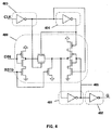
- step 100 a simple mixed (gate and switch) level circuit constituting a latch with asynchronous reset signal is shown.
- the circuit is split into channel connected components 400, 401, 402, 403, and 404.
- step 101 a structural loop between the CCCs 400 and 401 is identified and broken at net 405 with a pair of temporary boolean variables v0 and v1.
- F1 !CLK & RST0 & DIN
- step 103 the loop signature is computed, yielding the value of 9.
- step 104 it is established that a match is found with the predefined loop signatures from FIG. 3. Thus, step 105 is not executed.
- step 109 the loop signature identifies the loop as sequential, and, as an example only, the following Verilog code is generated:
Landscapes
- Engineering & Computer Science (AREA)
- Computer Hardware Design (AREA)
- Physics & Mathematics (AREA)
- Theoretical Computer Science (AREA)
- Evolutionary Computation (AREA)
- Geometry (AREA)
- General Engineering & Computer Science (AREA)
- General Physics & Mathematics (AREA)
- Design And Manufacture Of Integrated Circuits (AREA)
- Test And Diagnosis Of Digital Computers (AREA)
Abstract
Description
- A net which is an input to a CCC currently being explored is marked; or
- A net which is an input to a CCC currently being explored is a part of a CCC which is marked.
- Boolean function names start with an upper-case letter, e.g. F0, X1, Z1;
- Boolean variable names start with a lower-case letter, e.g. v0, v1;
- Boolean negation is denoted by the operator '!';
- Boolean conjunction is denoted by the operator '&';
- Boolean disjunction is denoted by the operator '|';
- (F depends on v) is a function that returns 1 if the value of F when v=0 is different from the value of F when v=1, and 0 otherwise.
Claims (12)
- A method of analysing a circuit, the circuit having at least one structural loop between different channel connected components within the circuit, the method comprising the steps of:at least partly notionally splitting the circuit into its constituent channel connected components;detecting the at least one structural loop;inserting a pair of temporary boolean variables at a break point on a boundary between different channel connected components to notionally break the at least one structural loop;analysing each channel connected component in the at least one structural loop utilising the pair of temporary boolean variables at the break point in order to obtain a pair of boolean functions representing the functionality of the circuit at the at least one break point;analysing the pair of boolean functions, including determining whether the at least one structural loop is sequential in nature; andmodifying the pair of boolean functions when the at least one structural loop is sequential in nature in order to remove any dependence in the pair of boolean functions on the pair of boolean variables.
- A method of analysing a circuit according to claim 1, further comprising the step of utilising the pair of boolean functions to produce an RTL description of the circuit in any desired RTL language.
- A method of analysing a circuit according to either claim 1 or claim 2, wherein the circuit includes at least one transistor-level component.
- A method of analysing a circuit according to either claim 1 or claim 2, wherein the circuit includes at least one gate-level component.
- A method of analysing a circuit according to claim 1, wherein the step of analysing the pair of boolean functions comprises:reformulating each of the pair of boolean functions to have at least a first term which is independent of both of the boolean variables, at least a second term dependent on one of the boolean variables, and at least a third term which is dependent on the inverse of said one of the boolean variables, wherein any of the terms may be zero; anddetermining whether the second term is non-zero and whether the third term is zero, in which case the at least one structural loop is sequential in nature.
- A method of analysing a circuit according to claim 5, wherein the step of modifying the boolean functions involves setting the second term to zero.
- A method of analysing a circuit according to claim 1, wherein the step of analysing the pair of boolean functions includes determining whether the at least one structural loop is combinational in nature.
- A method of analysing a circuit according to claim 7, wherein the step of determining whether the at least one structural loop is combinational in nature comprises:reformulating each of the pair of boolean functions to have at least a first term which is independent of both of the boolean variables, at least a second term dependent on one of the boolean variables, and at least a third term which is dependent on the inverse of said one of the boolean variables, wherein any of the terms may be zero; anddetermining whether both the second and third terms are zero, in which case the at least one structural loop is combinational in nature.
- A method of analysing a circuit according to claim 1, wherein the step of analysing the pair of boolean functions includes determining whether the at least one structural loop is oscillatory in nature.
- A method of analysing a circuit according to claim 9, further comprising the step of outputting a signal indicating that the circuit includes an oscillatory loop when the at least one structural loop is oscillatory in nature.
- A method of analysing a circuit according to claim 9, wherein the step of determining whether the at least one structural loop is oscillatory in nature comprises:reformulating each of the pair of boolean functions to have at least a first term which is independent of both of the boolean variables, at least a second term dependent on one of the boolean variables, and at least a third term which is dependent on the inverse of said one of the boolean variables, wherein any of the terms may be zero; anddetermining whether the third term is non-zero, in which case the at least one structural loop is oscillatory in nature.
- A method of analysing a circuit according to claim 1, wherein the step of analysing the pair of boolean functions includes the steps of:determining a loop signature for the at least one structural loop by combing each boolean function when dependent on a different one of the pair of boolean variables having different bias values, so as to obtain a unique signature for each possible combination of terms;determining whether the unique signature is one of a set of predetermined unique values; andmaking each of the boolean functions dependent on only one of the boolean variables by replacing the other of the boolean variables by an inverse of the one of the boolean variables, when the loop signature is not one of the set of predetermined unique values.
Applications Claiming Priority (2)
| Application Number | Priority Date | Filing Date | Title |
|---|---|---|---|
| US393988 | 1982-06-30 | ||
| US09/393,988 US6711534B1 (en) | 1999-09-10 | 1999-09-10 | Method of analyzing a circuit having at least one structural loop between different channel connected components within the circuit |
Publications (2)
| Publication Number | Publication Date |
|---|---|
| EP1083501A2 true EP1083501A2 (en) | 2001-03-14 |
| EP1083501A3 EP1083501A3 (en) | 2005-01-12 |
Family
ID=23557074
Family Applications (1)
| Application Number | Title | Priority Date | Filing Date |
|---|---|---|---|
| EP00119261A Withdrawn EP1083501A3 (en) | 1999-09-10 | 2000-09-06 | A method of analyzing a circuit having at least one structural loop between different channel connected components within the circuit |
Country Status (2)
| Country | Link |
|---|---|
| US (1) | US6711534B1 (en) |
| EP (1) | EP1083501A3 (en) |
Families Citing this family (4)
| Publication number | Priority date | Publication date | Assignee | Title |
|---|---|---|---|---|
| US6907587B2 (en) * | 1999-10-08 | 2005-06-14 | Dupont Photomasks, Inc. | System and method for correcting connectivity errors in a mask layout file |
| US7073141B2 (en) * | 2003-11-25 | 2006-07-04 | Intel Corporation | Device, system and method for VLSI design analysis |
| US7299431B2 (en) * | 2005-03-07 | 2007-11-20 | Lsi Corporation | Method for tracing paths within a circuit |
| US9817929B1 (en) | 2014-06-04 | 2017-11-14 | Calypto Design Systems, Inc. | Formal verification using microtransactions |
Family Cites Families (7)
| Publication number | Priority date | Publication date | Assignee | Title |
|---|---|---|---|---|
| US5210699A (en) | 1989-12-18 | 1993-05-11 | Siemens Components, Inc. | Process for extracting logic from transistor and resistor data representations of circuits |
| US5084824A (en) | 1990-03-29 | 1992-01-28 | National Semiconductor Corporation | Simulation model generation from a physical data base of a combinatorial circuit |
| US5640328A (en) * | 1994-04-25 | 1997-06-17 | Lam; Jimmy Kwok-Ching | Method for electric leaf cell circuit placement and timing determination |
| US5629858A (en) | 1994-10-31 | 1997-05-13 | International Business Machines Corporation | CMOS transistor network to gate level model extractor for simulation, verification and test generation |
| US5677848A (en) | 1995-11-03 | 1997-10-14 | Lucent Technologies Inc. | Method to derive the functionality of a digital circuit from its mask layout |
| US6014510A (en) * | 1996-11-27 | 2000-01-11 | International Business Machines Corporation | Method for performing timing analysis of a clock circuit |
| US6295636B1 (en) * | 1998-02-20 | 2001-09-25 | Lsi Logic Corporation | RTL analysis for improved logic synthesis |
-
1999
- 1999-09-10 US US09/393,988 patent/US6711534B1/en not_active Expired - Fee Related
-
2000
- 2000-09-06 EP EP00119261A patent/EP1083501A3/en not_active Withdrawn
Also Published As
| Publication number | Publication date |
|---|---|
| EP1083501A3 (en) | 2005-01-12 |
| US6711534B1 (en) | 2004-03-23 |
Similar Documents
| Publication | Publication Date | Title |
|---|---|---|
| EP0600608B1 (en) | Design verification method for programmable logic design | |
| Ashenden | Digital design (verilog): An embedded systems approach using verilog | |
| Bogliolo et al. | Regression-based RTL power modeling | |
| US7818158B2 (en) | Method for symbolic simulation of circuits having non-digital node voltages | |
| US20080201671A1 (en) | Method for generating timing exceptions | |
| US7292970B1 (en) | Finding unexercised logic for use in code coverage testing | |
| US6550041B1 (en) | Method and apparatus for evaluating the design quality of network nodes | |
| US6560571B1 (en) | Method and apparatus for prioritizing the order in which checks are performed on a node in an integrated circuit | |
| JP2008511894A (en) | Method and system for designing a structure level description of an electronic circuit | |
| US6305003B1 (en) | System and method for propagating clock nodes in a netlist of circuit design | |
| Kam et al. | Comparing layouts with HDL models: A formal verification technique | |
| US6711534B1 (en) | Method of analyzing a circuit having at least one structural loop between different channel connected components within the circuit | |
| US6449578B1 (en) | Method and apparatus for determining the RC delays of a network of an integrated circuit | |
| US7031889B1 (en) | Method and apparatus for evaluating the design quality of network nodes | |
| US6308301B1 (en) | System and method for detecting multiplexers in a circuit design | |
| Klein et al. | An efficient framework for high-level power exploration | |
| Hoskote et al. | Automatic verification of implementations of large circuits against HDL specifications | |
| US20030079190A1 (en) | Method for deriving a hierarchical functional description of a circuit | |
| US6260180B1 (en) | System and method for detecting FETs that are susceptible to bootstrapping | |
| US5677848A (en) | Method to derive the functionality of a digital circuit from its mask layout | |
| US6301691B1 (en) | System and method for detecting NFETs that pull up to VDD and PFETs that pull down to ground | |
| US6711722B1 (en) | Method for deriving a functional circuit description | |
| Meyer et al. | Active timing multilevel fault-simulation with switch-level accuracy | |
| US6542860B1 (en) | System and method for detecting nodes that are susceptible to floating | |
| US6367057B1 (en) | Method of analyzing a circuit having at least one structural loop within a channel connected component |
Legal Events
| Date | Code | Title | Description |
|---|---|---|---|
| PUAI | Public reference made under article 153(3) epc to a published international application that has entered the european phase |
Free format text: ORIGINAL CODE: 0009012 |
|
| AK | Designated contracting states |
Kind code of ref document: A2 Designated state(s): AT BE CH CY DE DK ES FI FR GB GR IE IT LI LU MC NL PT SE |
|
| AX | Request for extension of the european patent |
Free format text: AL;LT;LV;MK;RO;SI |
|
| PUAL | Search report despatched |
Free format text: ORIGINAL CODE: 0009013 |
|
| AK | Designated contracting states |
Kind code of ref document: A3 Designated state(s): AT BE CH CY DE DK ES FI FR GB GR IE IT LI LU MC NL PT SE |
|
| AX | Request for extension of the european patent |
Extension state: AL LT LV MK RO SI |
|
| AKX | Designation fees paid | ||
| REG | Reference to a national code |
Ref country code: DE Ref legal event code: 8566 |
|
| STAA | Information on the status of an ep patent application or granted ep patent |
Free format text: STATUS: THE APPLICATION IS DEEMED TO BE WITHDRAWN |
|
| 18D | Application deemed to be withdrawn |
Effective date: 20050713 |