EP1083500A2 - A method of analyzing a circuit having at least one structural loop within a channel connected component - Google Patents
A method of analyzing a circuit having at least one structural loop within a channel connected component Download PDFInfo
- Publication number
- EP1083500A2 EP1083500A2 EP00119260A EP00119260A EP1083500A2 EP 1083500 A2 EP1083500 A2 EP 1083500A2 EP 00119260 A EP00119260 A EP 00119260A EP 00119260 A EP00119260 A EP 00119260A EP 1083500 A2 EP1083500 A2 EP 1083500A2
- Authority
- EP
- European Patent Office
- Prior art keywords
- channel connected
- connected component
- boolean
- analysing
- equations
- Prior art date
- Legal status (The legal status is an assumption and is not a legal conclusion. Google has not performed a legal analysis and makes no representation as to the accuracy of the status listed.)
- Withdrawn
Links
Images



Classifications
-
- G—PHYSICS
- G06—COMPUTING OR CALCULATING; COUNTING
- G06F—ELECTRIC DIGITAL DATA PROCESSING
- G06F30/00—Computer-aided design [CAD]
- G06F30/30—Circuit design
- G06F30/32—Circuit design at the digital level
- G06F30/33—Design verification, e.g. functional simulation or model checking
Definitions
- This invention relates to a method of analyzing a circuit having at least one structural loop within a single channel connected component within the circuit, especially, though not exclusively, for use in Computer-Aided Design (CAD) tools for Electronic Design Automation (EDA), and more particularly for deriving equivalent behaviour of mixed (gate and switch) level digital circuits.
- CAD Computer-Aided Design
- EDA Electronic Design Automation
- the Register-Transfer Level describes a circuit at the high level of boolean functions and data flow within the circuit much like a regular programming language does.
- Gate-level descriptions provide a structural (schematic) description of a circuit as an interconnection of basic blocks called gates, whereas every gate has a known and relatively simple boolean behavior.
- Switch-level descriptions represent the lowest level of circuit design abstraction which again is a structural (schematic) one and contains an interconnection of switches (transistors) that implement the desired functionality of the circuit.
- RTL is often the preferred abstraction level for most design activities. However, any RTL design has to be translated into an equivalent switch-level design as a necessary step prior to the fabrication of the chip. This translation can be performed using so-called synthesis EDA tools that compile RTL designs into a predefined, technology-specific gate-level cell library that contains a switch-level schematic for each cell. In some cases, especially when a chip has to meet stringent operating requirements (speed, power consumption, etc.), certain blocks of the chip may be designed at the switch level.
- a very important application of such a technology is formal functional verification of circuits.
- Formal functional verification aims to ensure that a chip operates as expected based on appropriate mathematical models.
- formal verification provides 100% coverage of a circuit's functionality.
- a method is required to translate the structural description of a circuit into a functional (Boolean) description in the corresponding mathematical model.
- Other application areas for mixed (switch and gate) level circuit analysis and translation include technology-specific library characterization, Automatic Test Pattern Generation (ATPG), and re-synthesis and re-design of chips from one chip manufacturing technology to another.
- CCC Channel Connected Components
- a key aspect in deriving a functional model of a single CCC is the ability to identify and properly characterise the behaviour introduced by structural dependency loops within CCCs in the circuit.
- a structural loop within a CCC occurs when one or more transistors and/or one or more gates in the CCC is/are controlled by one or more nets that are also within that CCC. Such nets are referred to as internal inputs of the CCC, in contrast to the external inputs of the CCC, which are outputs of other CCCs and thus do not belong to the CCC.
- Structural loops within a CCC may result in combinational, sequential, or oscillatory behaviour.
- ANAMOS and TRANALYZE tools were developed at the Carnegie Mellon University for the purpose of transistor-level simulation and mapping into a hardware-based gate-level simulator and cannot properly analyse designs which contain sequential behaviour in a single CCC. This essentially prohibits the interaction of ANAMOS and TRANALYZE with the majority of the currently available EDA CAD tools.
- the present invention therefore seeks to provide a method of analysing a circuit having at least one structural loop within a channel connected component, which overcomes, or at least reduces the above-mentioned problems of the prior art.
- the invention provides a method of analysing a circuit, the circuit having at least one structural loop within a channel connected component, the method comprising the steps of:
- the result produced in the step of solving the system of Boolean equations can, conveniently, depend on the number of solutions that the system of Boolean equations has.
- a result that indicates that the system of Boolean equations has no solutions represents oscillatory behaviour in the channel connected component
- a result that indicates that the system of Boolean equations has a single solution represents combinational behaviour in the channel connected component
- a result that indicates that the system of Boolean equations has more than one solution represents sequential behaviour in the channel connected component
- the method preferably further comprises the step of outputting a signal indicating that the channel connected component exhibits oscillatory behaviour.
- the method preferably further comprises the step of utilising the single solution to produce an RTL representation of the channel connected component in any desired RTL language.
- the method preferably further comprises the steps of:
- the pairs of Boolean functions are utilised to produce an RTL representation of the channel connected component in any desired RTL language.
- an embodiment of the present invention contains a number of algorithmic steps.
- the following description assumes that the circuit being analysed has already been split into its constituent CCCs using known graph-based techniques (see the article "Boolean Analysis of MOS Circuits" by R. E. Bryant published in IEEE TCAD, 6(4), pp. 634-649, July 1987).
- the embodiment to be described here is concerned with deriving the equivalent behaviour of a CCC that contains structural loops.
- Such a CCC is schematically represented in FIG. 3, and has a number of external inputs 300 and outputs 301.
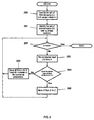
- step 100 in FIG. 1 structural loops in the CCC are detected.
- One particular approach is to identify the internal inputs to that CCC.
- an internal input is a net that controls a gate of a transistor or an input of a logic gate that are members of that CCC, and the net itself belongs to that CCC.
- step 100 is further illustrated in FIG. 3.
- Each structural loop is logically broken at the internal inputs by associating a pair of boolean variables (302) u i and d i representing the pull-up and pull-down conditions at the corresponding internal input, respectively.
- a system of Boolean equations B is formed.
- Known techniques for example, explicit path enumeration, are used to obtain the actual pull-up and pull-down functions U i and D i , at each internal input, with respect to the Boolean variables e i assigned to the external inputs 300 and the pairs of Boolean variables u i and d i assigned to the internal inputs.
- steps 102, 104, and 105 a known technique, for example Gaussian elimination, is used to either establish the solvability or solve the system of Boolean equations B with respect to one or more of the unknown entities.
- Gaussian elimination a known technique, for example Gaussian elimination, is used to either establish the solvability or solve the system of Boolean equations B with respect to one or more of the unknown entities.
- step 102 a check is made whether the system of Boolean equations B has at least one solution. If the system B has no solutions, then the CCC cannot reach a stable state, which corresponds to an oscillating behaviour, and a signal is output to the user in step 103. If it is established that system B has at least one solution, step 104 is executed next.
- step 104 a check is made whether the system of Boolean equations B has exactly one solution. If system B has exactly one solution, then the behaviour of the CCC is uniquely determined by the values of the Boolean variables e i and thus the CCC exhibits combinational behaviour. If the system of Boolean equations B has exactly one solution, step 106 is executed, otherwise step 105 is executed prior to step 106.
- step 105 it is known that the system of equations B has more than one solution. This means that, although the signals in the CCC can reach a stable state, that state is not uniquely determined by the values of the Boolean variables e i and thus the CCC exhibits sequential behaviour. Thus, it is necessary to identify the internal inputs that store the state of the CCC. Step 105 is described in more detail by the flow chart in FIG. 2, which itself contains seven steps.
- step 200 the set of pairs of Boolean variables u i and d i that have unique solutions are identified, and the corresponding internal inputs are put in the set of nets C. This set of internal inputs identifies those which do not store a state.
- step 201 all internal inputs that are not members of C are put into another set of internal inputs X for further examination in subsequent steps.
- step 202 the number of internal inputs in X is examined; step 105 is finished when X becomes empty. If there is at least one internal input in X, step 203 is executed.
- step 203 an internal input N is chosen from the set X.
- step 204 a check is made whether the system of Boolean equations B has a unique solution with respect to the pair of Boolean variables u N and d N . If such a unique solution exists, step 206 is executed, otherwise, step 205 is executed.
- step 205 the internal input N is added to the set of state storing nets S.
- N represents an independent input in the CCC
- its pair of boolean variables u N and d N are no longer treated as unknown entities but rather as additional parameters in the system of Boolean equations B.
- step 206 the internal input N is added to the set of nets C that are not storing a state in the CCC.
- Steps 202, 203, 204, 205, and 206 are executed until every internal input is either a member of S (and thus identified as a state storing net) or a member of C (and thus identified as a net that does not store a state).
- step 106 the derived CCC behaviour is represented in an RTL language.
- a separate approach is used for the nets that store a state and those that do not store a state.
- the solution of the system of Boo lean equations B with respect to the corresponding pair of Boolean variables u N and d N represents the pull-up and pull-down conditions for the net N.
- the equivalent RTL statements in the Verilog language are given as:
- the system of Boolean equations B is solved with respect to the corresponding pair of Boolean variables u N and d N thus obtaining the functions UX N and DX N , respectively.
- the latter two functions express the conditions under which the state storing net N may be pulled up or down, respectively.
- the function UX N & DX N therefore represents the condition under which the state storing net may have a value of 0 or 1, or, in other words, keeps its previous value.
- the function !UX N represents the condition that the net is pulled to 0 by the CCC
- the function !DX N represents the condition that the net is pulled to 1 by the CCC.
- the pair of boolean variables u N and d N serve as parameters in B, the actual pull-up and pull-down functions UX N and DX N may contain references to that pair of Boolean variables.
- the pair of Boolean variables u N and d N are universally quantified out using known Boolean function manipulation techniques (such as a Binary Decision Diagram representation) from both UX N and DX N , thus deriving UX' N and DX' N , respectively.
- Boolean function manipulation techniques such as a Binary Decision Diagram representation
- FIG. 4 the method described above is illustrated as applied to a simple mixed (switch and gate) level circuit implementing a latch with an asynchronous reset signal.
- the latch has three input ports 400, and a single output port 401.
- the whole example circuit comprises a single CCC containing the transistors 404 and 405 as well as the AND gate 406.
- the CCC contains one structural loop 402 with the internal input being net 403. There is no internal CCC loop between the transistors 404 and 405 as the input port Clk serves as an external input to the CCC of the latch.
- step 100 the CCC of the latch is checked for the presence of structural loops and net 403 is identified as an internal input.
- the loop is broken logically at net 403 by assigning the pair of variables u 0 and d 0 to that net.
- step 101 the following system of Boolean equations is produced:
- step 102 the system of Boolean equations is found to have a solution, thus step 104 is executed.
- step 104 the system of Boolean equations is found to have more than one solution, therefore, step 105 (and respectively 200) is executed next.
- step 200 the set C is found to be empty.
- step 201 the set X is found to contain the net 403. Since X is currently non-empty, the check at step 202 indicates that step 203 is to be executed. In step 203, the only net in X (net 403) is picked.
- step 204 Since the check in step 204 establishes that the system of Boolean equations does not have a unique solution with respect to the pair of Boolean variables u 0 and d 0 , step 205 is executed; net 403 is moved into the set S and X becomes empty. The following check in step 202 succeeds, which ends the execution of step 105.
- step 106 output is generated for net 403 only.
- net 403 is a state storing net (member of S)
- UX 0 and DX 0 are computed as:
- extracted higher-level model for designs containing static memory storage do not contain unknown net values and closely resembles the structure of the original mixed-level design.
Landscapes
- Engineering & Computer Science (AREA)
- Computer Hardware Design (AREA)
- Physics & Mathematics (AREA)
- Theoretical Computer Science (AREA)
- Evolutionary Computation (AREA)
- Geometry (AREA)
- General Engineering & Computer Science (AREA)
- General Physics & Mathematics (AREA)
- Design And Manufacture Of Integrated Circuits (AREA)
- Test And Diagnosis Of Digital Computers (AREA)
Abstract
Description
- Boolean function names start with an upper-case letter, e.g. F0, X1, Z1;
- Boolean variable names start with a lower-case letter, e.g. v0, v1;
- Boolean negation is denoted by the operator '!';
- Boolean conjunction is denoted by the operator '&';
- Boolean disjunction is denoted by the operator '|'.
- DX'0 = !(Din & !Clk)
- UX'0 = !(!Din & !Clk | !RB & (!Din | Clk))
- trireg net403;
- assign net403 = Din & !Clk ? 1'b1 : 1'bz;
- assign net403 = !Din & !Clk | !RB & ( !Din | Clk) ? 1'b0 : 1'bz;
Claims (9)
- A method of analysing a circuit, the circuit having at least one structural loop within a channel connected component, the method comprising the steps of:at least partly notionally splitting the circuit into its constituent channel connected components;detecting at least one structural loop within a channel connected component;inserting a pair of temporary boolean variables at a break point in the at least one structural loop at an internal input within the channel connected component;repeating the step of inserting a pair of temporary boolean variables for each detected structural loop within the channel connected component;analysing the channel connected component utilising the pairs of temporary boolean variables at the break points in order to obtain a pair of boolean equations at each break point representing the functionality of the channel connected component at that break point to produce a system of boolean equations for the break points within the channel connected component; andsolving the system of boolean equations to produce a result that indicates whether the channel connected component has oscillatory, combinational or sequential behaviour.
- A method of analysing a circuit according to claim 1, wherein the result produced in the step of solving the system of boolean equations depends on the number of solutions that the system of boolean equations has.
- A method of analysing a circuit according to claim 2, wherein a result that indicates that the system of boolean equations has no solutions represents oscillatory behaviour in the channel connected component.
- A method of analysing a circuit according to claim 3, further comprising the step of outputting a signal indicating that the channel connected component exhibits oscillatory behaviour when the result indicates that the system of boolean equations has no solutions.
- A method of analysing a circuit according to claim 2, wherein a result that indicates that the system of boolean equations has a single solution represents combinational behaviour in the channel connected component.
- A method of analysing a circuit according to claim 5, further comprising the step of utilising the single solution to produce an RTL representation of the channel connected component in any desired RTL language when the result indicates that the system of boolean equations has a single solution.
- A method of analysing a circuit according to claim 2, wherein a result that indicates that the system of boolean equations has more than one solution represents sequential behaviour in the channel connected component.
- A method of analysing a circuit according to claim 7, further comprising, when the result indicates that the system of boolean equations has more than one solution, the steps of:determining which internal inputs are coupled solely to data storage elements in the channel connected component and which internal inputs are at least partly dependent on external inputs to the channel connected component;replacing the temporary boolean variables by predetermined parameters at the break point in the at least one structural loop at each internal input which is coupled solely to data storage elements in the channel connected component; andresolving the system of boolean equations using the predetermined parameters in place of the temporary boolean variables that were replaced to produce a pair of boolean functions for each of the internal inputs that are at least partly dependent on an external input.
- A method of analysing a circuit according to claim 8, further comprising utilising the pairs of boolean functions to produce an RTL representation of the channel connected component in any desired RTL language.
Applications Claiming Priority (2)
| Application Number | Priority Date | Filing Date | Title |
|---|---|---|---|
| US09/393,629 US6367057B1 (en) | 1999-09-10 | 1999-09-10 | Method of analyzing a circuit having at least one structural loop within a channel connected component |
| US393629 | 1999-09-10 |
Publications (2)
| Publication Number | Publication Date |
|---|---|
| EP1083500A2 true EP1083500A2 (en) | 2001-03-14 |
| EP1083500A3 EP1083500A3 (en) | 2005-01-12 |
Family
ID=23555565
Family Applications (1)
| Application Number | Title | Priority Date | Filing Date |
|---|---|---|---|
| EP00119260A Withdrawn EP1083500A3 (en) | 1999-09-10 | 2000-09-06 | A method of analyzing a circuit having at least one structural loop within a channel connected component |
Country Status (2)
| Country | Link |
|---|---|
| US (1) | US6367057B1 (en) |
| EP (1) | EP1083500A3 (en) |
Families Citing this family (1)
| Publication number | Priority date | Publication date | Assignee | Title |
|---|---|---|---|---|
| US10176286B1 (en) * | 2017-03-17 | 2019-01-08 | Cadence Design Systems, Inc. | System, method, and computer program product for oscillating loop detection in formal verification |
Family Cites Families (9)
| Publication number | Priority date | Publication date | Assignee | Title |
|---|---|---|---|---|
| US5210699A (en) | 1989-12-18 | 1993-05-11 | Siemens Components, Inc. | Process for extracting logic from transistor and resistor data representations of circuits |
| US5084824A (en) | 1990-03-29 | 1992-01-28 | National Semiconductor Corporation | Simulation model generation from a physical data base of a combinatorial circuit |
| US5446676A (en) * | 1993-03-29 | 1995-08-29 | Epic Design Technology Inc. | Transistor-level timing and power simulator and power analyzer |
| US5640328A (en) * | 1994-04-25 | 1997-06-17 | Lam; Jimmy Kwok-Ching | Method for electric leaf cell circuit placement and timing determination |
| US5629858A (en) | 1994-10-31 | 1997-05-13 | International Business Machines Corporation | CMOS transistor network to gate level model extractor for simulation, verification and test generation |
| US5677848A (en) | 1995-11-03 | 1997-10-14 | Lucent Technologies Inc. | Method to derive the functionality of a digital circuit from its mask layout |
| US6014510A (en) * | 1996-11-27 | 2000-01-11 | International Business Machines Corporation | Method for performing timing analysis of a clock circuit |
| US6185723B1 (en) * | 1996-11-27 | 2001-02-06 | International Business Machines Corporation | Method for performing timing analysis of a clock-shaping circuit |
| US5946475A (en) * | 1997-01-21 | 1999-08-31 | International Business Machines Corporation | Method for performing transistor-level static timing analysis of a logic circuit |
-
1999
- 1999-09-10 US US09/393,629 patent/US6367057B1/en not_active Expired - Fee Related
-
2000
- 2000-09-06 EP EP00119260A patent/EP1083500A3/en not_active Withdrawn
Also Published As
| Publication number | Publication date |
|---|---|
| US6367057B1 (en) | 2002-04-02 |
| EP1083500A3 (en) | 2005-01-12 |
Similar Documents
| Publication | Publication Date | Title |
|---|---|---|
| US5831869A (en) | Method of compacting data representations of hierarchical logic designs used for static timing analysis | |
| EP0600608B1 (en) | Design verification method for programmable logic design | |
| US7076748B2 (en) | Identification and implementation of clock gating in the design of integrated circuits | |
| US6952812B2 (en) | Design analysis tool for path extraction and false path identification and method thereof | |
| US7003738B2 (en) | Process for automated generation of design-specific complex functional blocks to improve quality of synthesized digital integrated circuits in CMOS using altering process | |
| US5946475A (en) | Method for performing transistor-level static timing analysis of a logic circuit | |
| WO1995034036A2 (en) | Method and apparatus for estimating the power dissipated by a digital circuit | |
| US6922665B1 (en) | Method and system for device-level simulation of a circuit design for a programmable logic device | |
| Chappell et al. | LAMP: Logic‐Circuit Simulators | |
| US6560571B1 (en) | Method and apparatus for prioritizing the order in which checks are performed on a node in an integrated circuit | |
| Turner et al. | DILL: Specifying digital logic in LOTOS | |
| US6077305A (en) | Latch inference using dataflow analysis | |
| US6874134B1 (en) | Conversion of an HDL sequential truth table to generic HDL elements | |
| US5774380A (en) | State capture/reuse for verilog simulation of high gate count ASIC | |
| US6308301B1 (en) | System and method for detecting multiplexers in a circuit design | |
| CN114880975A (en) | Hardware trojan generation method, system, equipment and medium | |
| US7031889B1 (en) | Method and apparatus for evaluating the design quality of network nodes | |
| Glebov et al. | False-noise analysis using resolution method | |
| US6157903A (en) | Method of minimizing macrocell characterization time for state dependent power analysis | |
| US20030079190A1 (en) | Method for deriving a hierarchical functional description of a circuit | |
| Hoskote et al. | Automatic verification of implementations of large circuits against HDL specifications | |
| Devadas et al. | Verification of asynchronous interface circuits with bounded wire delays | |
| US6367057B1 (en) | Method of analyzing a circuit having at least one structural loop within a channel connected component | |
| US6711534B1 (en) | Method of analyzing a circuit having at least one structural loop between different channel connected components within the circuit | |
| US6711722B1 (en) | Method for deriving a functional circuit description |
Legal Events
| Date | Code | Title | Description |
|---|---|---|---|
| PUAI | Public reference made under article 153(3) epc to a published international application that has entered the european phase |
Free format text: ORIGINAL CODE: 0009012 |
|
| AK | Designated contracting states |
Kind code of ref document: A2 Designated state(s): AT BE CH CY DE DK ES FI FR GB GR IE IT LI LU MC NL PT SE |
|
| AX | Request for extension of the european patent |
Free format text: AL;LT;LV;MK;RO;SI |
|
| PUAL | Search report despatched |
Free format text: ORIGINAL CODE: 0009013 |
|
| AK | Designated contracting states |
Kind code of ref document: A3 Designated state(s): AT BE CH CY DE DK ES FI FR GB GR IE IT LI LU MC NL PT SE |
|
| AX | Request for extension of the european patent |
Extension state: AL LT LV MK RO SI |
|
| AKX | Designation fees paid | ||
| REG | Reference to a national code |
Ref country code: DE Ref legal event code: 8566 |
|
| STAA | Information on the status of an ep patent application or granted ep patent |
Free format text: STATUS: THE APPLICATION IS DEEMED TO BE WITHDRAWN |
|
| 18D | Application deemed to be withdrawn |
Effective date: 20050713 |