EP1083458A2 - Lens-fitted film unit with strobe circuit - Google Patents
Lens-fitted film unit with strobe circuit Download PDFInfo
- Publication number
- EP1083458A2 EP1083458A2 EP00307601A EP00307601A EP1083458A2 EP 1083458 A2 EP1083458 A2 EP 1083458A2 EP 00307601 A EP00307601 A EP 00307601A EP 00307601 A EP00307601 A EP 00307601A EP 1083458 A2 EP1083458 A2 EP 1083458A2
- Authority
- EP
- European Patent Office
- Prior art keywords
- trigger
- strobe
- light
- capacitor
- main
- Prior art date
- Legal status (The legal status is an assumption and is not a legal conclusion. Google has not performed a legal analysis and makes no representation as to the accuracy of the status listed.)
- Withdrawn
Links
Images






Classifications
-
- G—PHYSICS
- G03—PHOTOGRAPHY; CINEMATOGRAPHY; ANALOGOUS TECHNIQUES USING WAVES OTHER THAN OPTICAL WAVES; ELECTROGRAPHY; HOLOGRAPHY
- G03B—APPARATUS OR ARRANGEMENTS FOR TAKING PHOTOGRAPHS OR FOR PROJECTING OR VIEWING THEM; APPARATUS OR ARRANGEMENTS EMPLOYING ANALOGOUS TECHNIQUES USING WAVES OTHER THAN OPTICAL WAVES; ACCESSORIES THEREFOR
- G03B15/00—Special procedures for taking photographs; Apparatus therefor
- G03B15/02—Illuminating scene
- G03B15/03—Combinations of cameras with lighting apparatus; Flash units
- G03B15/05—Combinations of cameras with electronic flash apparatus; Electronic flash units
-
- G—PHYSICS
- G03—PHOTOGRAPHY; CINEMATOGRAPHY; ANALOGOUS TECHNIQUES USING WAVES OTHER THAN OPTICAL WAVES; ELECTROGRAPHY; HOLOGRAPHY
- G03B—APPARATUS OR ARRANGEMENTS FOR TAKING PHOTOGRAPHS OR FOR PROJECTING OR VIEWING THEM; APPARATUS OR ARRANGEMENTS EMPLOYING ANALOGOUS TECHNIQUES USING WAVES OTHER THAN OPTICAL WAVES; ACCESSORIES THEREFOR
- G03B19/00—Cameras
- G03B19/02—Still-picture cameras
- G03B19/04—Roll-film cameras
-
- G—PHYSICS
- G03—PHOTOGRAPHY; CINEMATOGRAPHY; ANALOGOUS TECHNIQUES USING WAVES OTHER THAN OPTICAL WAVES; ELECTROGRAPHY; HOLOGRAPHY
- G03B—APPARATUS OR ARRANGEMENTS FOR TAKING PHOTOGRAPHS OR FOR PROJECTING OR VIEWING THEM; APPARATUS OR ARRANGEMENTS EMPLOYING ANALOGOUS TECHNIQUES USING WAVES OTHER THAN OPTICAL WAVES; ACCESSORIES THEREFOR
- G03B2215/00—Special procedures for taking photographs; Apparatus therefor
- G03B2215/05—Combinations of cameras with electronic flash units
- G03B2215/0503—Built-in units
Definitions
- the present invention relates to a strobe circuit, to which another electronic circuit or electronic element is added, and a printed circuit board for strobe, which comprises two circuit boards, and also relates to a lens-fitted film unit and a camera, which incorporates the abovementioned strobe circuit or printed-circuit board for strobe.
- FIG. 1 shows an example of the strobe circuit diagram employed for such lens-fitted film units.
- Fig. 1 when main switches S 1 , S 2 are turned ON by an external operation, the electronic current, fed from battery B, flows into transistor T R trough register R 1 to start the oscillation, by which the high-voltage of 300-350 volts is induced at the secondary winding of oscillation transformer T.
- the induced electronic current from the secondary winding is rectified by diode D, and the rectified electronic current flows into main-capacitor C M and trigger-capacitor C T , serially connected with register R 1 , to charge them.
- main-capacitor C M is charged to a predetermined voltage, light-emitting diode D L , serially connected with register R 2 , emits light.
- trigger-switch S T turns ON in conjunction with the opening operation of shutter blinds. Then, the closed circuit, including trigger-capacitor C T , trigger-switch S T , the primary winding of trigger-transformer T C and main switches S 1 , S 2 , is formed to discharge the electronic charge stored in trigger-capacitor C T . As a result, the further high-voltage is induced in the secondary winding of trigger-transformer T C , and the induced high-voltage is applied to the trigger-electrode of xenon tube Xe, in which electrons, isolated from the cathode, impinge with ionized xenon atoms to excite the xenon atoms. Thus, xenon tube Xe emits the strobe light associating with the discharging action of main-capacitor C M .
- the lens-fitted film unit Since it is a primary subject for the lens-fitted film unit to reduce its price as low as possible, it is difficult to equip various kinds of image capturing mechanisms in it. Nevertheless, consumers desire that more image capturing mechanisms are incorporated in the lens-fitted film unit, in order to enjoy the image capturing with better photographic images.
- the strobe circuit is utilized only for activating the strobe lighting in such lens-fitted film units, as a matter of course.
- the parts, included in the strobe circuit are relatively expensive, and the battery and the main-capacitor require large spaces. Therefore, it has been quite wasteful for lens-fitted film units to limit the purpose of the strobe circuit within the strobe lighting.
- the first object of the present invention to provide a strobe device, which makes it possible to equip a new function in the strobe device by adding a little electronic circuit or some electronic parts to the fundamental circuit for strobe lighting.
- the second object of the present invention is to provide a combination of two printed circuit boards, strictly coupled each other, which is disposed in a vacant space of a lens-fitted film unit or a camera.
- the abovementioned objects of the present invention can be attained by a strobe device, a lens-fitted film unit and a camera described as follow.
- Fig. 8 shows an exploded perspective view of the lens-fitted film unit.
- the lens-fitted film unit is comprised of unit main-body 91, front cover 921, rear cover 931, photographic lens 95, shutter unit 96, etc.
- Shutter unit 96, photographic lens 95, etc. are mounted in unit main-body 91, which is covered with front cover 921 and rear cover 931.
- unit main-body 91 comprises an exposed film chamber in which a film magazine is accommodated.
- the lens-fitted film unit comprises a strobe device for capturing images with strobe lighting.
- the strobe device embodied in the present invention, comprises a light-emitting tube to emit a strobe light, a main-capacitor coupled to the light-emitting tube in parallel so as to supply a light emitting energy to the light-emitting tube, a trigger-transformer to apply a trigger-voltage onto the trigger-electrode of the light-emitting tube, a trigger-means, registers, a trigger-capacitor connected to the main-capacitor through the register to discharge an electric charge into the trigger-transformer when the trigger-means turns ON, and an operating section (operating means) driven by a part of the electric charge stored in the main-capacitor, which flows through the register at the time of the strobe lighting when the trigger-means turns ON.
- strobe device will be also referred to as "strobe circuit” in the following description. It is desirable that the light emitting energy, supplied to the light-emitting tube by the main-capacitor, is the high-voltage energy. In addition, it is also desirable that the trigger-voltage, applied to the trigger-electrode by the trigger-transformer, is the high-voltage.
- a xenon tube can be referred to a typical example of the light-emitting tube, while a trigger-switch, a thyristor and a transistor can be referred to desirable and concrete examples of the trigger-means.
- the trigger-means turns ON in conjunction with the opening operation of the shutter.
- a zener diode serving as a constant-voltage generating element, and a light-emitting diode can be referred to desirable examples of it.
- the constant-voltage generating element such as a zener diode, etc.
- the constant-voltage generating element does not necessarily generate a strictly constant voltage with little margin, but generates a substantially constant voltage within a predetermined voltage range.
- the zener diode is sufficiently applicable for the strobe device, embodied in the present invention. It is desirable that the anode of the zener diode is coupled to the negative electrode of the main-capacitor.
- the light-emitting diode when the light is emitted from the light-emitting diode by the electronic current flowing in it, the operating means is regarded as entering in the activated state. It is desirable that the cathode of the light-emitting diode is coupled to the negative electrode of the main-capacitor.
- an added circuit driven by the voltage source generated by the constant-voltage generating element, is coupled to it in parallel.
- a light-intensity regulating circuit which controls the intensity of the strobe light, emitted from the strobe device, in response to an amount of strobe light reflect from the subject, to be detailed later, can be referred to the added circuit.
- the closed circuit serially connecting the trigger-capacitor, the trigger-switch, and the primary winding of the trigger-transformer, is formed, and, at the same time, the closed circuit, serially connecting the main-capacitor, the operating means, the register, the trigger-switch and the primary winding of the trigger-transformer, is formed.
- the lens-fitted film unit further comprises a power source to supply electronic power to the strobe device.
- the power source is a battery of 1-2 volt, and specifically desirable a dry battery of 1.5 volt.
- the strobe device embodied in the present invention, even if the operating means, having a certain added value, is equipped in the strobe device, it is possible to supply a driving energy to the operating means merely by utilizing the normal power source such as a dry battery of 1-2 volt, employed for conventional strobe devices, without employing another power source for the operating means. Therefore, it becomes possible to provide a strobe device of high added value and low cost.
- the strobe device comprises a first printed board on which electronic parts, constituting basic strobe-electronic circuits to perform at least the voltage boosting, the electronic charging and the light emitting, are mounted, and a second printed board on which electronic parts, constituting electronic circuits other than the basic strobe-electronic circuits, are mounted.
- the first printed board and the second printed board are coupled each other by a conductive member having conductivity, and the light-intensity regulating circuit is equipped on the second printed board.
- the voltage-boosting circuit and the light-emitting circuit are equipped on the first printed board, and, in this case, the first printed board and the second printed board are coupled each other by at least two conductive members.
- a predetermined electronic circuit can be easily added to the basic strobe-electronic circuits, in order to grade up the function of the apparatus concerned. Therefore, it becomes possible to easily manufacture plural kinds of strobe devices without providing many manufacturing lines and without a lot of man-hours for management, even if plural kinds of strobe devices are manufactured in an independent site.
- the present invention is not only applicable for the lens-fitted film unit, but also applicable for all fields of strobe devices, of course, including a camera incorporated with the strobe device and a digital camera incorporated with the strobe device.
- the strobe circuit which employs the light-emitting diode for the operating means, will be detailed as a first embodiment of the present invention. Then, the strobe circuit, which employs the constant-voltage generating element (the zener diode) for the operating means, and comprises the light-intensity regulating circuit, will be detailed as a second embodiment of the present invention.
- a light source for discriminating a type of print is added to the strobe device.
- the IX240 film is so constituted that aspect ratios of photographic prints, namely, the three print types including C, H, P, are selectable, when capturing and printing images.
- Type H represents a print type having a Hi-Vision size of slightly long sideways and the largest negative image area.
- Type C represents a print type having a conventional size, which is similar to the standard image area of the 135 film, formed by excluding both right and left edge portions of the type H negative image area.
- Type P represents a print type having a panorama size, whose sideways are extraordinarily long, formed by excluding both upper and lower edge portions of the type H negative image area.
- the user selects the print type after loading the IX240 film in the camera
- the user selects anyone of types C, H, P by externally operating the camera.
- the viewing area of the selected print type is displayed in the finder, and the selected print type is recorded on the film outside the photographic image area, in response to shutter release action of the user.
- This recording action is achieved by either a magnetic-recording method when the camera comprises a magnetic-recording head, or an optical-recording method when the camera does not comprise the magnetic-recording head.
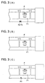
- FIG. 2(a), Fig. 2(b), Fig. 2(c), Fig. 3(a), Fig. 3(b) and Fig. 3(c) an example of the abovementioned optical-recording method, by which one of print types C, H, P is recorded on the IX240 film, is detailed in the following.
- Fig. 2(a), Fig. 2(b) and Fig. 2(c) show enlarged cross-sectional views of a recording section, which records the selected print type on the IX240 film, and specifically, Fig. 2(a), Fig. 2(b) and Fig. 2(c) corresponds to selection of type C, selection of type H and selection of type P, respectively.
- Fig. 3(a), Fig. 3(b) and Fig. 3(c) show views of the IX240 film, on which images are recorded corresponding to the selected print type, and specifically, Fig. 3(a), Fig. 3(b) and Fig. 3(c) corresponds to selection of type C, selection of type H and selection of type P, respectively.
- numeral 11 indicates a light guide, made of transparent acrylic acid resin, etc., to guide a light emitted from a light-emitting diode located at right side (not shown in the drawings) in the direction indicated by the arrow. Therefore, the light emitted from the light-emitting diode is finally emitted from light-emitting terminals 11a, 11b.
- Numeral 12 indicates a shading plate, which has two through-holes 12a, 12b and slides in its longitudinal directions (both right and left directions), corresponding to the selecting operation of the user.
- Numeral 1d indicates a sidewall of the unit main-body equipped with various kinds of photographic functions, and sidewall 1d has two through-holes 1m, 1n located opposite light-emitting terminals 11a, 11b.
- the IX240 film (hereinafter, referred to as film F) is positioned at the rear side of sidewall 1d.
- shading plate 12 slides to such a position that through-holes 12a, 12b are located opposite light-emitting terminals 11a, 11b of the light guide 11 and through-holes 1m, 1n of sidewall 1d. Accordingly, the light emitted from light-emitting terminals 11a, 11b exposes film F after traveling through through-holes 12a, 12b and through-holes 1m, 1n. Then, as shown in Fig. 3(a), two marks F2 and F3 are exposed outside photographic image F1 on film F.
- shading plate 12 slides to such a position that through-holes 12a, 12b are located apart from light-emitting terminals 11a, 11b of the light guide 11 and through-holes 1m, 1n of sidewall 1d. Accordingly, the light emitted from light-emitting terminals 11a, 11b is shaded by shading plate 12. Then, as shown in Fig. 3(b), no mark is exposed on film F.
- shading plate 12 slides to such a position that through-hole 12a is located opposite light-emitting terminal 11b of the light guide 11 and through-hole 1n of sidewall 1d. Accordingly, the light emitted from light-emitting terminal 11b exposes film F after traveling through through-hole 12a and through-hole 1n, while the light emitted from light-emitting terminal 11a is shaded by shading plate 12. Then, as shown in Fig. 3(c), only mark F3 is exposed outside photographic image F1 on film F.
- a strobe circuit which incorporates the abovementioned light-emitting diode, will be detailed in the following.
- trigger-switch S T When capturing image, trigger-switch S T turns ON in conjunction with the opening operation of shutter blinds. Then, the closed circuit, serially connecting trigger-capacitor C T , trigger-switch S T , the primary winding of trigger-transformer T C and main switches S 1 , S 2 , is formed to discharge the electronic charge, stored in trigger-capacitor C T , into the primary winding of trigger-transformer T C .
- xenon tube Xe emits the strobe light associating with the discharging action of main-capacitor C M .
- trigger-switch S T turns ON, another closed circuit, serially connecting main-capacitor C M , light-emitting diode D G , register R 3 , trigger-switch S T and the primary winding of trigger-transformer T C , is formed, at the same time when the abovementioned closed circuit, including trigger-capacitor C T , is formed.
- trigger-switch S T turns ON
- a part of electronic charge, stored in main-capacitor C M flows into register R 3 through the primary winding of trigger-transformer T C and trigger-switch S T , resulting in electronic current i 1 .
- a part of electronic charge, stored in main-capacitor C M also flows into register R 3 , so as to charge trigger-capacitor C T , resulting in electronic current i 2 .
- electronic current i 1 is greater than electronic current i 2
- the luminous duration time of light-emitting diode D G is shorter than the duration time of ON state of trigger-switch S T , and is around 500 ⁇ sec., which is substantially equivalent to the luminous duration time of xenon tube Xe.
- two light-emitting diodes D G are serially connected in the abovementioned strobe circuit, and two light guides are provided for guiding a light of each light-emitting diode D G , as a individual light guide, instead of light guide 11 shown in Figs. 2(a), 2(b) and 2(c).
- the light-intensity regulating circuit which regulates a luminous duration time of the xenon tube in response to the intensity of returned strobe light reflected from the subject, is added to the strobe circuit.
- the strobe circuit with the light-intensity regulating circuit will be detailed in the following.
- Capacitor C P is serially coupled to photo-sensor Ph, and zener diode D T is coupled to them in parallel.
- the connected point of capacitor C P and photo-sensor Ph is coupled to the base of transistor T RP with register R4, while the emitter of transistor T RP is coupled to the gate of thyristor S.
- Thyristor S is serially coupled to choke-coil C C , serving as a current dumper, and xenon tube Xe is coupled to them in parallel.
- the electronic charge stored in main-capacitor C M rushes into choke-coil C C with an electronic current far greater than that of flowing into xenon tube Xe to consume the electronic charge in choke-coil C C , resulting in deactivation of the illumination of xenon tube Xe.
- the inductance of choke-coil C C is in a range of 2-20 ⁇ H and the peak current, flowing into choke-coil C C , is in a range of 5-10 times of the current flowing into xenon tube Xe.
- choke-coil C C rapidly consumes the electronic charge stored in main-capacitor C M in mid-course of illuminating action of xenon tube Xe.
- the illuminating action of xenon tube Xe is stopped within a shorter luminous duration time.
- transistor T RP slowly turns ON to activate thyristor S
- the illuminating action of xenon tube Xe is stopped within a longer luminous duration time.
- strobe circuits added with the light source for discriminating the print type and added with the light-intensity regulating circuit are described as embodiments of the present invention in the above, the scope of the present invention is not limited to the abovementioned embodiments.
- a power saving strobe circuit having a function of automatically stopping charging-action, a counter circuit for counting number of times of strobe lighting, which is referred to recycling of the strobe device, and a date exposing circuit for exposing date on the photographic image can be also driven by the zener voltage generated between both terminals of the zener diode.
- circuits can be mounted on a printed-circuit board, which is incorporated in lens-fitted film units or cameras.
- Fig. 6 shows a perspective view of a main body of the lens-fitted film unit
- Fig. 7 shows an enlarged cross-sectional view of two printed-circuit boards coupled each other.
- numeral 1 indicates a main body incorporating various kinds of photographic mechanisms.
- Numeral 1a indicates an exposing section, which holds photographic lens L, and includes a shutter mechanism (not shown in the drawings) to expose images on a non-exposed film loaded interior main body 1 by means of a shutter release mechanism.
- Numeral 1b indicates a film rolling chamber, in which a non-exposed film roll is mounted, while Numeral 1c indicates a film cartridge chamber, which includes a film cartridge, and winds a exposed film into the film cartridge by means of a winding mechanism (not shown in the drawings).
- Numeral 2 indicates a strobe unit
- Numeral 21 indicates a first printed-circuit board on which parts, constituting the fundamental strobe circuit as shown in Fig. 1, are mounted, and main-capacitor 22, having a large dimension, is also attached.
- strobe lighting section 23 is also fixed on the first printed-circuit board 21.
- Numeral 26 indicates a second printed-circuit board on which parts, constituting one of the aforementioned added circuits, are mounted. Second printed-circuit board 26 is coupled to first printed-circuit board 21 by means of at least two conductive members 27 having conductivity.
- Strobe unit 2 is attached to main body 1 in a manner such that first printed-circuit board 21 is arranged between exposing section 1a and film rolling chamber 1b, and main-capacitor 22 is arranged below exposing section 1a, and strobe lighting section 23 is arranged at upper side of film rolling chamber 1b.
- first printed-circuit board 21 is arranged between exposing section 1a and film rolling chamber 1b
- main-capacitor 22 is arranged below exposing section 1a
- strobe lighting section 23 is arranged at upper side of film rolling chamber 1b.
- second printed-circuit board 26 is also arranged at this space.
- conductive member 27, which connects first printed-circuit board 21 and second printed-circuit board 26 each other, can be formed in such a manner that two parts of a wire is bended to form stopper sections 27a, and both edges of the wire are soldered to connect both printed-circuit boards. Since each of the soldering positions is located at a part of conductive circuit pattern, it is possible to electrically connect first printed-circuit board 21 to second printed-circuit board 26 by means of conductive members 27, number of which are equivalent to number of electrical connections necessary between them. At the same time, it is also possible to mechanically hold first printed-circuit board 21 and second printed-circuit board 26 with a predetermined space by means of conductive members 27.
- a bar-type axial material having conductivity, can be also employed for conductive members 27, instead of the wire material.
- second printed-circuit board 26 is not limited to the position between exposing section 1a and film rolling chamber 1b, but it is also possible to arrange it at such a position being backside of strobe lighting section 23 and in the upper space of film rolling chamber 1b.
- second printed-circuit board 26 is not necessary in parallel with first printed-circuit board 21, but it is also applicable that, for instance, second printed-circuit board 26 is coupled to first printed-circuit board 21 in an orthogonal direction.
- an added printed-circuit board on which parts for one of various kinds of added circuits are mounted, can be attached to the strobe circuit board provided with fundamental circuits for strobe lighting, to provide such strobe units as a light-intensity regulating strobe unit which can vary an amount of strobe light by stopping the illuminating action in mid-course of strobe lighting corresponding to the object distance, an automatic charge-stopping strobe unit which can automatically stops charging action when completing the charge of the capacitor, and an automatic illuminating strobe unit which automatically emits strobe light only when the luminance of the subject is lower than the predetermined luminance.
- Fig. 9 shows a perspective view of a strobe unit, viewing from front side;
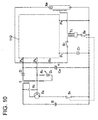
- Fig. 10 shows a fundamental circuit-diagram of a strobe unit;
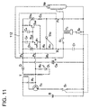
- Fig. 11 shows a circuit-diagram of a strobe unit added with a circuit for regulating a light-intensity of the strobe light;
- Fig. 12 shows a circuit-diagram of a strobe unit added with a circuit for automatically stopping the charging action;
- Fig. 13 shows a circuit-diagram of a strobe unit added with a circuit for automatically emitting strobe light.
- numeral 111 indicates a printed-circuit board for strobe lighting, on which a voltage-boosting circuit, utilized for boosting up the voltage of power source, and fundamental parts, utilized for the illumination circuit to start the illumination of the discharge tube, are mounted.
- a voltage-boosting circuit utilized for boosting up the voltage of power source
- fundamental parts utilized for the illumination circuit to start the illumination of the discharge tube
- Numeral 114 indicates an illuminating section, which includes a discharge tube, a reflector, a strobe panel, etc., and is attached to printed-circuit board 111.
- Numeral 115 indicates a main-capacitor, mounted on printed-circuit board 111 by means of two lead wires.
- bar materials, wires, plate materials, and etc. can be employed for connecting members 113, as far as such materials can mechanically support added printed-circuit board 112 and are conductive between both conductive printed-patterns as needed.
- photo-receiving element 116 is mounted on added printed-circuit board 112 as needed, and notch 16a, through which a light beam enters into photo-receiving element 116, is formed in printed circuit board 111.
- added printed-circuit board 112 is not necessary in parallel with printed-circuit board 111, but it is also applicable that, for instance, added printed-circuit board 112 is coupled to printed-circuit board 111 in an orthogonal direction or etc.
- connecting members 113 would be formed in a bended-shape and/or the edge sidewall portion of connecting members 113 would be attached to added printed-circuit board 112.
- a hard printed circuit board made of paper-phenol resin or grass-epoxy resin can be employed for both printed-circuit board 111 and added printed-circuit board 112, and a flexible printed circuit board made of polyester resin also can be employed as well.
- main-switch S 1 When main-switch S 1 is turned ON by an external operation and illumination-prohibiting switch S 2 is also turned ON in conjunction with main-switch S 1 , the electronic current, fed from battery B, flows into transistor T R trough register R 1 to start the oscillation, by which the high-voltage of 300-350 volts is induced at the secondary winding of oscillation transformer T.
- the induced electronic current from the secondary winding is rectified by diode D, and the rectified electronic current flows into main-capacitor C M and trigger-capacitor C T , serially connected with register R 1 , to charge them.
- main-capacitor C M When main-capacitor C M is charged to a predetermined voltage, light-emitting diode D L , serially connected with register R 2 , emits light.
- trigger-switch S T When capturing image, trigger-switch S T turns ON in conjunction with the opening operation of shutter blinds. Then, the closed circuit, serially connecting trigger-capacitor C T , trigger-switch S T , the primary winding of trigger-transformer T C and illumination-prohibiting switch S 2 , is formed, to discharge the electronic charge, stored in trigger-capacitor C T , into the primary winding of trigger-transformer T C .
- discharge tube Xe emits the strobe light associating with the discharging action of main-capacitor C M .
- circuits are mounted in printed circuit board 111, and symbols Pa, Pb, Pc and Pd indicate connecting ports for connecting it to added printed-circuit board 112 by means of connecting members 113.
- Connecting ports Pa, Pb, Pc and Pd are coupled to the negative electrode of main-capacitor C M , the base of transistor T R , the connecting point of capacitor C T and register R 3 , and the positive electrode of main-capacitor C M , respectively.
- Fig. 11 the circuit diagram, added with a light-intensity regulating circuit, will be detailed in the following.
- the embodiment, shown in Fig. 11, is an example in which the zener diode is employed as the operating means.
- the parts, constituting the light-intensity regulating circuit are mounted on light-intensity regulating circuit board 112.
- trigger-switch S T turns ON, a part of electronic charge, stored in main-capacitor C M , flows into register R 11 , which is coupled to port Pc, through the primary winding of trigger-transformer T C and trigger-switch S T , resulting in electronic current i 1 .
- trigger-capacitor C T after trigger-capacitor C T is discharged, a part of electronic charge, stored in main-capacitor C M , also flows into register R 11 , so as to charge trigger-capacitor C T , resulting in electronic current i 2 .
- electronic current i 0 since the anode of zener diode D 11 is coupled to the negative pole of main-capacitor C M and the cathode of zener diode D 11 is serially coupled to registers R 11 , R 12 , electronic current i 0 , which is equal to i 1 + i 2 , flows into zener diode D 11 .
- Capacitor C P is serially coupled to phototransistor P T , and zener diode D 11 , the anode of which is coupled to port Pa, is coupled to them in parallel.
- Phototransistor P T which is equivalent to photo-receiving element 16 shown in Fig. 9, receives a light reflected from the subject.
- the connected point of capacitor C P and phototransistor Ph is coupled to the base of transistor T RP with register R 13 , while the emitter of transistor T RP is coupled to the gate of thyristor Th 1 .
- Thyristor Th 1 is serially coupled to choke-coil C C , one end of which is coupled to port Pd, and discharge tube Xe is coupled to them in parallel.
- Thyristor Th 2 is inserted between the connecting point of registers R 11 , R 12 and one end of choke-coil C C , so as to prevent instability of the electronic current, due to chattering actions of trigger-switch S T , when it turns ON.
- capacitor C Z is inserted for suppressing trigger noises.
- the automatic charge-stopping circuit is equipped on added printed-circuit board 112.
- the charged voltage of main-capacitor C M reaches the zener-voltage (for instance, 300-350 volts) of zener diode D 21 , anode of which is coupled to port Pa
- an electronic current flows into zener diode D21 through the collector of transistor T 21 , which is coupled to port Pd, allowing that transistor T 21 turns ON.
- the base voltage of transistor T R is lowered, resulting in deactivation of the oscillation with transistor T R and stoppage of the charging action for main-capacitor CM.
- the emitter of transistor T 21 is coupled to port Pb, while nothing is coupled to port Pc.
- photo-receiving element 116 is excluded from the circuit.
- main-capacitor C M since the charging action for main-capacitor C M is automatically stopped when the charged voltage of it reaches a predetermined voltage, the power dissipation of battery B can be lowered.
- a circuit-diagram in which an automatic illuminating circuit is equipped as the added circuit for the fundamental strobe circuit, will be detailed in the following.
- the automatic illuminating circuit is equipped on added printed-circuit board 112.
- CdS cell Cd serving as photo-receiving element 116, is serially connected to register R31, and one end of CdS cell Cd is coupled to port Pd, while one end of register R31 is coupled to port Pc.
- noting is coupled to ports Pa, Pb.
- discharge tube Xe does not emit any light, while discharge tube Xe emits light, when the luminance of the subject is low.
- the electronic parts for each of three types of added circuits are mounted on the added printed-circuit board.
- the scope of the present invention is not limited to the above embodiment. It is also applicable to integrally assemble the electronic parts in a package and to mount the package on the added printed-circuit board.
- different types of strobe units can be manufactured by interchangeably mounting various kinds of main parts on the printed circuit board, which is already equipped with the fundamental circuit for strobe lighting.
- Fig. 14 shows a perspective view of the strobe unit, viewing from backside.
- Numeral 121 indicates a printed-circuit board for strobe lighting, on which a voltage-boosting circuit, utilized for boosting up the voltage of power source, and fundamental parts, utilized for the illumination circuit to start the illumination of the discharge tube and etc., are mounted.
- Numeral 131 indicates a illuminating section, including the discharge tube, the reflector, the strobe panel, etc., the distribution characteristic of luminous intensity of which corresponds to the viewing angle of the standard photographic lens. In addition, illuminating section 131 is attached to printed-circuit board 121.
- lens-fitted film units of a new type introducing a wide-angle lens, merely by changing a minimum number of other parts.
- illuminating section 132 in which the distribution characteristic of luminous intensity is arranged for the wide viewing angle by changing at least a reflector, is provided in advance, and then, as a replacement of illuminating section 131, illuminating section 132 is attached to printed circuit board 121, corresponding to the wide-angle lens employed.
- different types of strobe units can be manufactured in the same production line and process.
- the distribution characteristic of luminous intensity is merely one of various examples. Any kinds of distribution characteristics of luminous intensity are applicable, as far as the distribution characteristic of luminous intensity of illuminating section 131 is different from that of illuminating section 132.
- numeral 133 indicates a main-capacitor, which is equipped on printed circuit board 121. It is possible to shorten the charging time of the main-capacitor and/or to reduce the cost of the strobe unit, by employing the main-capacitor having a smaller capacity, when employing a photographic lens having a brighter F-number and/or accommodating a film having a higher sensitivity. For this purpose, as a replacement of main-capacitor 133, the main-capacitor 134, having a capacity smaller than that of main-capacitor 133, is mounted on printed circuit board 121, corresponding to the F-number of the photographic lens and/or the sensitivity of the film. Thus, different types of strobe units can be manufactured in the same production line and process.
- any kinds of capacitors are applicable, as far as each of the capacitors, having different capacities, can be interchangeably mounted on printed circuit board 121, it is desirable that a diameter and a pitch of the two lead wires are coincided between different capacitors, since the two lead wires are inserted into the holes of printed circuit board 121 and fixed on it by soldering process.
- numeral 122 indicates a battery-contacting plate for negative pole
- numeral 135 indicates a battery-contacting plate for positive pole, one end of which is fixed on printed circuit board 121. Size AA battery B3 is held between battery-contacting plates 122, 135.
- main-capacitor 134 having a small capacity is equipped on printed circuit board 121, it is possible to employ size AAA battery B4 having a smaller capacity, instead of size AA battery B3.
- battery-contacting plate 135 can be also replaced by battery contacting plate 136 having a length shorter than that of battery-contacting plate 135 to hold size AAA battery B4 between battery-contacting plates 122, 136. Accordingly, it is possible to change size AA battery B3 to size AAA battery B4 merely by changing battery-contacting plate 135 to battery-contacting plate 136.
- different types of strobe units can be manufactured in the same production line and process.
- the battery-contacting plate for positive pole which can hold the size N battery, is also applicable, as needed.
- the battery-contacting plate to be interchangeably mounted, is not necessary that for positive pole. It is also possible that various kinds of battery-contacting plates for negative pole are interchanged as needed, while fixing the battery-contacting plate for positive pole.
- the main body, on which the strobe unit, described above, is equipped, may be either a lens-fitted film unit, a conventional camera being possible to change film, or a digital camera.
- the strobe circuit embodied in the present invention, it is possible to activate the operating means, added to the strobe circuit, synchronized with the illuminating action of the xenon tube, as well as to reduce a number of parts utilized for the operating means.
- the strobe circuit embodied in the present invention, it is possible to activate the operating means, added to the strobe circuit, synchronized with activation of the trigger-switch, as well as to reduce a number of parts utilized for the operating means.
- the strobe circuit, the lens-fitted film unit and the camera, embodied in the present invention it is possible to activate the light-emitting diode, synchronized with activation of the trigger-switch.
- the strobe circuit embodied in the present invention, it is possible to activate the zener diode, synchronized with activation of the trigger-switch.
- the strobe circuit embodied in the present invention, it is possible to activate the added circuit, using the zener diode as the power source of it.
- the strobe circuit, the lens-fitted film unit and the camera embodied in the present invention, it is possible to activate the light-intensity regulating circuit, using the zener diode as the power source of it.
- the strobe circuit, the lens-fitted film unit and the camera embodied in the present invention, it is possible to add the circuit to the second printed circuit board, without major modification of the printed circuit board already mounting the fundamental circuit for strobe lighting.
Landscapes
- Physics & Mathematics (AREA)
- General Physics & Mathematics (AREA)
- Stroboscope Apparatuses (AREA)
- Structure And Mechanism Of Cameras (AREA)
Abstract
Description
Claims (18)
- A strobe device, comprising:a strobe light-emitting tube to emit a strobe light;a main-capacitor coupled in parallel to said strobe light-emitting tube, so as to supply a luminous energy to said strobe light-emitting tube;a trigger-transformer to apply a trigger-voltage to a trigger-electrode of said strobe light-emitting tube;a trigger-section to activate a light-emitting action of said strobe light-emitting tube;a trigger-capacitor, coupled to said main-capacitor with a register, to store an electronic charge, which is discharged to said trigger-transformer when said trigger-section turns ON; andan operating section driven by a part of an electronic charge, stored in said main-capacitor, flowing through said register when said trigger-section turns ON to activate said light-emitting action of said strobe light-emitting tube.
- The strobe device of claim 1,
wherein a closed circuit, serially connecting said trigger-capacitor, said trigger-section and a primary winding of said trigger-transformer, is formed when said trigger-section turns ON, and simultaneously, another closed circuit, serially connecting said main-capacitor, said operating section, said register, said trigger-section and said primary winding of said trigger-transformer, is formed. - The strobe device of claim 1,
wherein said operating section is a constant-voltage generating element. - The strobe device of claim 3,
wherein said constant-voltage generating element is a zener diode. - The strobe device of claim 4,
wherein an anode of said zener diode is coupled to a negative pole of said main-capacitor. - The strobe device of claim 3,
wherein an added circuit, which is driven by a voltage-source generated by said constant-voltage generating element, is coupled in parallel to said constant-voltage generating element. - The strobe device of claim 6,
wherein said added circuit is a light-intensity regulating circuit, which controls an amount of said strobe light emitted from said strobe device, in response to an amount of said strobe light reflected from a subject. - The strobe device of claim 7, further comprising:a first printed circuit board on which electronic parts, constituting a fundamental circuit for a strobe lighting, including at least a voltage-boosting circuit, a charging circuit and a illumination circuit, are mounted; anda second printed circuit board on which electronic parts, constituting an electronic circuit other than said fundamental circuit, are mounted, wherein said first printed circuit board and said second printed circuit board are coupled each other by means of a conductive member having an electronic conductivity, and said light-intensity regulating circuit is equipped on said second printed circuit board.
- The strobe device of claim 8,
wherein said first printed circuit board and said second printed circuit board are coupled each other by means of at least said two conductive members. - The strobe device of claim 1,
wherein said operating section is a light-emitting diode. - The strobe device of claim 10,
wherein a cathode of said light-emitting diode is coupled to a negative pole of said main-capacitor. - A lens-fitted film unit equipped with a strobe device, comprising:a main-body;a photographic lens;a shutter; anda photographic film loaded in said main-body, wherein said strobe device comprises,a strobe light-emitting tube to emit a strobe light;a main-capacitor coupled in parallel to said strobe light-emitting tube, so as to supply a luminous energy to said strobe light-emitting tube;a trigger-transformer to apply a trigger-voltage to a trigger-electrode of said strobe light-emitting tube;a trigger-section to activate a light-emitting action of said strobe light-emitting tube;a trigger-capacitor, coupled to said main-capacitor with a register, to store an electronic charge, which is discharged to said trigger-transformer when said trigger-section turns ON; andan operating section driven by a part of an electronic charge, stored in said main-capacitor, flowing through said register when said trigger-section turns ON to activate said light-emitting action of said strobe light-emitting tube.
- The lens-fitted film unit of claim 12,
wherein said trigger-section turns ON in conjunction with a opening action of said shutter. - The lens-fitted film unit of claim 12,
wherein said operating section is a light-emitting diode, and a print type of a captured image is selectable by a photographer in said lens-fitted film unit, and said light-emitting diode exposes a mark, corresponding to said print type selected by said photographer, on an unexposed area, outside a photographic image area, of said photographic film. - The lens-fitted film unit of claim 12, further comprising:a power source to supply an electronic power to said strobe device, said power source is a battery of 1 - 2 volt.
- A camera equipped with a strobe device, comprising:a photographic lens; anda shutter, wherein said strobe device comprises,a strobe light-emitting tube to emit a strobe light;a main-capacitor coupled in parallel to said strobe light-emitting tube, so as to supply a luminous energy to said strobe light-emitting tube;a trigger-transformer to apply a trigger-voltage to a trigger-electrode of said strobe light-emitting tube;a trigger-section to activate a light-emitting action of said strobe light-emitting tube;a trigger-capacitor, coupled to said main-capacitor with a register, to store an electronic charge, which is discharged to said trigger-transformer when said trigger-section turns ON; andan operating section driven by a part of an electronic charge, stored in said main-capacitor, flowing through said register when said trigger-section turns ON to activate said light-emitting action of said strobe light-emitting tube.
- The camera of claim 16,
wherein said trigger-section turns ON in conjunction with a opening action of said shutter. - The camera of claim 16,
wherein said operating section is a light-emitting diode, and a print type of a captured image is selectable by a photographer in said camera, and said light-emitting diode exposes a mark outside a photographic image area of an unexposed film, corresponding to said print type selected by said photographer.
Applications Claiming Priority (4)
| Application Number | Priority Date | Filing Date | Title |
|---|---|---|---|
| JP25283999A JP2001075156A (en) | 1999-09-07 | 1999-09-07 | Strobo circuit, film unit with lens, camera, and printed circuit board for strobo |
| JP25283999 | 1999-09-07 | ||
| JP2000016955A JP3997679B2 (en) | 2000-01-26 | 2000-01-26 | Strobe unit |
| JP2000016955 | 2000-01-26 |
Publications (2)
| Publication Number | Publication Date |
|---|---|
| EP1083458A2 true EP1083458A2 (en) | 2001-03-14 |
| EP1083458A3 EP1083458A3 (en) | 2005-07-27 |
Family
ID=26540906
Family Applications (1)
| Application Number | Title | Priority Date | Filing Date |
|---|---|---|---|
| EP00307601A Withdrawn EP1083458A3 (en) | 1999-09-07 | 2000-09-04 | Lens-fitted film unit with strobe circuit |
Country Status (2)
| Country | Link |
|---|---|
| US (1) | US6466744B1 (en) |
| EP (1) | EP1083458A3 (en) |
Cited By (1)
| Publication number | Priority date | Publication date | Assignee | Title |
|---|---|---|---|---|
| EP1519221A1 (en) * | 2003-09-24 | 2005-03-30 | Fuji Photo Film Co., Ltd. | Lens-fitted photo film unit and manufacturing method thereof |
Families Citing this family (7)
| Publication number | Priority date | Publication date | Assignee | Title |
|---|---|---|---|---|
| US6633728B2 (en) * | 2000-09-25 | 2003-10-14 | Fuji Photo Film Co., Ltd. | Flash device, lens-fitted photo film unit, camera, and producing method for the same |
| EP1727400A1 (en) * | 2001-05-02 | 2006-11-29 | Fuji Photo Film Co., Ltd. | Flash device |
| US6871016B2 (en) * | 2001-12-27 | 2005-03-22 | Eastman Kodak Company | Recyclable camera and method for assembling same |
| US6574430B1 (en) * | 2001-12-27 | 2003-06-03 | Eastman Kodak Company | Camera electronic system and method of assembling same |
| US20070217779A1 (en) * | 2006-03-14 | 2007-09-20 | Haas William R | Recapture of electrical charge from a capacitor to a battery |
| JP5166001B2 (en) * | 2007-11-16 | 2013-03-21 | オンセミコンダクター・トレーディング・リミテッド | Light emitting element driving circuit and mobile phone |
| JP6700816B2 (en) * | 2016-02-02 | 2020-05-27 | キヤノン株式会社 | Lighting equipment |
Family Cites Families (5)
| Publication number | Priority date | Publication date | Assignee | Title |
|---|---|---|---|---|
| DE2166612B2 (en) * | 1970-08-24 | 1975-12-04 | Ponder & Best, Inc., Santa Monica, Calif. (V.St.A.) | Control device for determining the duration of an energy supply to a load |
| JPS5796319A (en) * | 1980-12-05 | 1982-06-15 | Olympus Optical Co Ltd | Photometric electric power supply device of automatic dimming stroboscope |
| US5038080A (en) * | 1989-04-25 | 1991-08-06 | West Electric Co., Ltd. | Electric flash apparatus |
| US5784658A (en) * | 1995-03-09 | 1998-07-21 | Fuji Photo Film Co., Ltd. | Optical data recording device of camera and lens-fitted photographic film unit |
| EP0757281B1 (en) * | 1995-07-31 | 1999-04-21 | Eastman Kodak Company | Optical data recording circuit for a photographic camera, powered by the camera's flash capacitor |
-
2000
- 2000-09-04 EP EP00307601A patent/EP1083458A3/en not_active Withdrawn
- 2000-09-07 US US09/656,798 patent/US6466744B1/en not_active Expired - Fee Related
Cited By (1)
| Publication number | Priority date | Publication date | Assignee | Title |
|---|---|---|---|---|
| EP1519221A1 (en) * | 2003-09-24 | 2005-03-30 | Fuji Photo Film Co., Ltd. | Lens-fitted photo film unit and manufacturing method thereof |
Also Published As
| Publication number | Publication date |
|---|---|
| US6466744B1 (en) | 2002-10-15 |
| EP1083458A3 (en) | 2005-07-27 |
Similar Documents
| Publication | Publication Date | Title |
|---|---|---|
| KR950033637A (en) | Photo film unit with lens and flash unit for use | |
| US6466744B1 (en) | Strobe circuit, lens-fitted film unit, camera and printed-circuit board for strobe | |
| US6724987B2 (en) | Lens-fitted photo film unit with electronic flash device | |
| US6339679B1 (en) | Single use camera with built-in electronic flash | |
| US20020012534A1 (en) | Fixed focus camera | |
| JP3997679B2 (en) | Strobe unit | |
| US6633728B2 (en) | Flash device, lens-fitted photo film unit, camera, and producing method for the same | |
| US6636700B2 (en) | Flash device, lens-fitted photo film unit, camera, light measuring device, and method of producing lens-fitted photo film unit | |
| US6061531A (en) | One-time use camera with strobe circuit baseboard | |
| JP4250351B2 (en) | Strobe device | |
| KR100227680B1 (en) | Flash circuit | |
| JP2001075156A (en) | Strobo circuit, film unit with lens, camera, and printed circuit board for strobo | |
| JP2847531B2 (en) | Film integrated camera | |
| JPS595853Y2 (en) | Automatic dimming electronic flash device | |
| JP2530218Y2 (en) | Film integrated camera | |
| JPH10161225A (en) | Information imprinting device of camera | |
| JP2001228512A (en) | Strobe unit and its manufacturing method | |
| JP2004021014A (en) | Camera | |
| JP2002341414A (en) | Stroboscopic device | |
| JPH10232433A (en) | Stroboscopic unit and film unit with lens provided with built-in stroboscope | |
| JPS5949523A (en) | camera control device | |
| EP1191825A2 (en) | Flash device for a camera | |
| JP2002169215A (en) | Stroboscope device and film unit or camera with lens using the same device and manufacturing method for the film unit with lens | |
| JP2002357860A (en) | Stroboscopic device | |
| JPH1195309A (en) | Optical data exposure circuit |
Legal Events
| Date | Code | Title | Description |
|---|---|---|---|
| PUAI | Public reference made under article 153(3) epc to a published international application that has entered the european phase |
Free format text: ORIGINAL CODE: 0009012 |
|
| AK | Designated contracting states |
Kind code of ref document: A2 Designated state(s): AT BE CH CY DE DK ES FI FR GB GR IE IT LI LU MC NL PT SE |
|
| AX | Request for extension of the european patent |
Free format text: AL;LT;LV;MK;RO;SI |
|
| PUAL | Search report despatched |
Free format text: ORIGINAL CODE: 0009013 |
|
| AK | Designated contracting states |
Kind code of ref document: A3 Designated state(s): AT BE CH CY DE DK ES FI FR GB GR IE IT LI LU MC NL PT SE |
|
| AX | Request for extension of the european patent |
Extension state: AL LT LV MK RO SI |
|
| 17P | Request for examination filed |
Effective date: 20060109 |
|
| AKX | Designation fees paid |
Designated state(s): DE FR GB |
|
| STAA | Information on the status of an ep patent application or granted ep patent |
Free format text: STATUS: THE APPLICATION IS DEEMED TO BE WITHDRAWN |
|
| 18D | Application deemed to be withdrawn |
Effective date: 20060728 |