EP1083144A1 - Micro-electromechanical structure insensitive to mechanical stresses. - Google Patents
Micro-electromechanical structure insensitive to mechanical stresses. Download PDFInfo
- Publication number
- EP1083144A1 EP1083144A1 EP99830565A EP99830565A EP1083144A1 EP 1083144 A1 EP1083144 A1 EP 1083144A1 EP 99830565 A EP99830565 A EP 99830565A EP 99830565 A EP99830565 A EP 99830565A EP 1083144 A1 EP1083144 A1 EP 1083144A1
- Authority
- EP
- European Patent Office
- Prior art keywords
- structure according
- anchoring portion
- microelectromechanical structure
- extending
- electrodes
- Prior art date
- Legal status (The legal status is an assumption and is not a legal conclusion. Google has not performed a legal analysis and makes no representation as to the accuracy of the status listed.)
- Granted
Links
Images


Classifications
-
- B—PERFORMING OPERATIONS; TRANSPORTING
- B81—MICROSTRUCTURAL TECHNOLOGY
- B81B—MICROSTRUCTURAL DEVICES OR SYSTEMS, e.g. MICROMECHANICAL DEVICES
- B81B3/00—Devices comprising flexible or deformable elements, e.g. comprising elastic tongues or membranes
- B81B3/0064—Constitution or structural means for improving or controlling the physical properties of a device
- B81B3/0067—Mechanical properties
- B81B3/0072—For controlling internal stress or strain in moving or flexible elements, e.g. stress compensating layers
-
- G—PHYSICS
- G01—MEASURING; TESTING
- G01C—MEASURING DISTANCES, LEVELS OR BEARINGS; SURVEYING; NAVIGATION; GYROSCOPIC INSTRUMENTS; PHOTOGRAMMETRY OR VIDEOGRAMMETRY
- G01C19/00—Gyroscopes; Turn-sensitive devices using vibrating masses; Turn-sensitive devices without moving masses; Measuring angular rate using gyroscopic effects
- G01C19/56—Turn-sensitive devices using vibrating masses, e.g. vibratory angular rate sensors based on Coriolis forces
- G01C19/567—Turn-sensitive devices using vibrating masses, e.g. vibratory angular rate sensors based on Coriolis forces using the phase shift of a vibration node or antinode
- G01C19/5677—Turn-sensitive devices using vibrating masses, e.g. vibratory angular rate sensors based on Coriolis forces using the phase shift of a vibration node or antinode of essentially two-dimensional [2D] vibrators, e.g. ring-shaped vibrators
- G01C19/5684—Turn-sensitive devices using vibrating masses, e.g. vibratory angular rate sensors based on Coriolis forces using the phase shift of a vibration node or antinode of essentially two-dimensional [2D] vibrators, e.g. ring-shaped vibrators the devices involving a micromechanical structure
-
- G—PHYSICS
- G01—MEASURING; TESTING
- G01P—MEASURING LINEAR OR ANGULAR SPEED, ACCELERATION, DECELERATION, OR SHOCK; INDICATING PRESENCE, ABSENCE, OR DIRECTION, OF MOVEMENT
- G01P15/00—Measuring acceleration; Measuring deceleration; Measuring shock, i.e. sudden change of acceleration
- G01P15/02—Measuring acceleration; Measuring deceleration; Measuring shock, i.e. sudden change of acceleration by making use of inertia forces using solid seismic masses
- G01P15/08—Measuring acceleration; Measuring deceleration; Measuring shock, i.e. sudden change of acceleration by making use of inertia forces using solid seismic masses with conversion into electric or magnetic values
- G01P15/0888—Measuring acceleration; Measuring deceleration; Measuring shock, i.e. sudden change of acceleration by making use of inertia forces using solid seismic masses with conversion into electric or magnetic values for indicating angular acceleration
-
- G—PHYSICS
- G01—MEASURING; TESTING
- G01P—MEASURING LINEAR OR ANGULAR SPEED, ACCELERATION, DECELERATION, OR SHOCK; INDICATING PRESENCE, ABSENCE, OR DIRECTION, OF MOVEMENT
- G01P15/00—Measuring acceleration; Measuring deceleration; Measuring shock, i.e. sudden change of acceleration
- G01P15/02—Measuring acceleration; Measuring deceleration; Measuring shock, i.e. sudden change of acceleration by making use of inertia forces using solid seismic masses
- G01P15/08—Measuring acceleration; Measuring deceleration; Measuring shock, i.e. sudden change of acceleration by making use of inertia forces using solid seismic masses with conversion into electric or magnetic values
- G01P15/125—Measuring acceleration; Measuring deceleration; Measuring shock, i.e. sudden change of acceleration by making use of inertia forces using solid seismic masses with conversion into electric or magnetic values by capacitive pick-up
-
- B—PERFORMING OPERATIONS; TRANSPORTING
- B81—MICROSTRUCTURAL TECHNOLOGY
- B81B—MICROSTRUCTURAL DEVICES OR SYSTEMS, e.g. MICROMECHANICAL DEVICES
- B81B2201/00—Specific applications of microelectromechanical systems
- B81B2201/02—Sensors
- B81B2201/0228—Inertial sensors
- B81B2201/0235—Accelerometers
-
- B—PERFORMING OPERATIONS; TRANSPORTING
- B81—MICROSTRUCTURAL TECHNOLOGY
- B81B—MICROSTRUCTURAL DEVICES OR SYSTEMS, e.g. MICROMECHANICAL DEVICES
- B81B2203/00—Basic microelectromechanical structures
- B81B2203/01—Suspended structures, i.e. structures allowing a movement
- B81B2203/0109—Bridges
Definitions
- the present invention regards a micro-electromechanical structure insensitive to mechanical stresses.
- surface and epitaxial micromachining techniques allow production of microstructures within a layer that is deposited (for example a polycrystalline silicon film), or grown (for example an epitaxial layer), on sacrificial regions, removed at the end of the manufacturing process, by wet etching.
- the layers subject to micromachining are formed at high temperatures, completely different from the operative temperatures.
- the various regions forming the end devices have different thermal expansion coefficients. Consequently, at the microstructure operative temperatures, residual mechanical stresses are present; in addition, in particular when the various regions are doped not uniformly, the stresses are not uniform (stress gradients); these stresses thus cause undesirable mechanical deformations of the microstructures, as described schematically hereinafter with reference to figures 1-6.
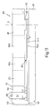
- figure 1 shows in cross-section a structure 1 comprising a polycrystalline silicon bridge element 2, formed on a monocrystalline silicon substrate 3; a sacrificial oxide layer 4 extends between the bridge element 2 and the substrate 3, except for two areas, where anchorage portions 5 of the bridge element 2 extend through the sacrificial oxide layer 4, and are supported directly on the substrate 3.
- Figure 2 shows the same structure 1 as in figure 1, in plan view.
- Figures 3 and 4 show the structure 1, after removal of the sacrificial oxide layer 4, when the dimensions of the structure have been reduced (shown exaggerated in the figures, for better understanding), owing to the presence of residual stress; in particular, in figure 3, owing to the different thermal coefficients, the dimensions of the bridge element 2 are reduced (shortened) more than those of the substrate 3; here the bridge element 2 is subjected to tensile stress, and assumes a more favorable energetic configuration.
- the bridge element 2 undergoes a lesser reduction of dimensions than the substrate 3; consequently, in this condition, the bridge element 2 tends to be lengthened in comparison with the substrate 3, but, owing to the fixed anchorage portions 5, it undergoes stress of a compressive type, causing buckling deformation.
- the average residual stress thus has the effect of modifying the resilient constant of the micromechanical structures; this modification is not reproducible, and can cause mechanical collapse of the structure (in particular in the case in figure 4).
- the projecting element 11 is formed on a monocrystalline silicon substrate 12; a sacrificial oxide layer 13 extends between the projecting element 11 and the substrate 12, except for an area, where an anchorage portion 14 of the projecting element 11 extends through the sacrificial oxide layer 13, and is supported directly on the substrate 12.
- Figure 6 shows the structure 10 of figure 5, after removal of the sacrificial oxide layer 13.
- the release of the residual stress gradient causes the projecting element 11 to flex.
- ⁇ R(z) the function linking the residual stress with the coordinate z in the projecting element 11
- ⁇ R the average residual stress
- ⁇ the strain gradient the strain gradient
- the material of the package has a different coefficient of thermal expansion as compared to the material of the micromechanical structure (mono- or polycrystalline silicon). Consequently, the suspended masses may be subject to small displacements with respect to the fixed regions of the micromechanical structure.
- the stresses inherently present in the materials or induced by packaging, by acting in a different and non-uniform way on the various anchorage points, causes tension in some parts and compression in other parts, such as to modify the mutual positions of these parts and to generate non-symmetrical geometries of the structures.
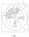
- Figure 7 shows a semiconductor material chip 20 housing an angular accelerometer 21 comprising a rotor 22 and a stator 23.
- the chip 20 may moreover house circuit components (not shown) for biasing, controlling and processing signals.
- the angular accelerometer 21 has a barycentric axis G (defined as an axis passing through the center of gravity - not shown) coinciding with the axis of symmetry of the accelerometer.
- the rotor 22 (which is able to perform micrometric rotations about the barycentric axis G, in such a way that every movement of the rotor is defined by instantaneous vectors perpendicular to the barycentric axis G) comprises a suspended mass 25 having an annular shape concentric to the barycentric axis G and bearing a plurality of mobile electrodes 26 extending radially inwards from the suspended mass 25. Each mobile electrode 26 is associated to two fixed electrodes 27, 28 extending radially, each of which faces a different side of the respective mobile electrode 26.
- the first capacitor and the second capacitor associated to a same mobile electrode 26 are, instead, connected in series.
- any movement of the suspended mass 25 brings about an increase in the capacitance of one of the two capacitors associated to each mobile electrode 26 and a reduction in the capacitance of the other capacitor. Consequently, by appropriately biasing the mobile electrodes 26 and the fixed electrodes 27, 28 and by connecting them to a circuit that measures the capacitance, it is possible to detect any movement of the suspended mass 25 with respect to the stator 23.
- each spring 30 comprises a pair of lateral arms 31 extending radially inwards from the suspended mass 25, at a distance from one another, and connected to one another at their radially inner ends by a cross portion 32.
- a central arm 33 thus extends radially from the center of the cross portion 32 between the side arms 31 for approximately one half of the length of the side arms 31 and terminates at the rotor anchorage region 34, which is integral with the chip 20.
- the springs 30 are suspended and hence are deformable as a result of the rotation of the suspended mass 25.
- FIG 8 moreover shows stator anchorage regions 35a, 35b integral with the fixed electrodes 27 and 28, respectively.
- the stator anchorage regions 35a, 35b have a width greater than the fixed electrodes 27, 28, extend in depth as far as the substrate (in a not shown manner), and protrude on the sides of the fixed electrodes 27, 28 not facing the respective mobile electrodes 26.
- a trench 38 separates the mobile mass 25 from the rest of the chip 20.
- the angular accelerometer 21 thus presents reduced performance in terms of sensitivity and precision.
- the variations in performance are non-uniform on components belonging to different batches and, at times, on components belonging to a same batch.
- the aim of the invention is thus to solve the problem described above.
- a micro-electromechanical structure is provided, as defined in Claim 1.
- an angular accelerometer 40 is integrated in a chip 41 of semiconductor material and has a general structure similar to that of Figure 7. Consequently, the parts of the accelerometer 40 of Figure 9 that are in common with those of the accelerometer 20 of Figure 7 are denoted by the same reference numbers and will not be further described.
- the suspended mass 25 of the angular accelerometer 40 is supported and biased by a suspension structure comprising four springs 44 and a single anchoring element 45.
- the springs 44 extend radially and are set 90° apart.
- the springs 44 extend between the suspended mass 25 and the anchoring element 45, and the latter is arranged concentrically with respect to the suspended mass 25 along the barycentric axis G of the angular accelerometer 40.
- the springs 44 preferably comprise a first, outer, portion 44a and a second, inner, portion 44b.
- the first portion 44a extends for approximately one third of the length of the spring 44, has a width greater than the second portion 44b (which in practice defines the elastic part that is deformed during rotation of the rotor 22), and is preferably perforated, as is the suspended mass 25, to enable releasing of the rotor 22.
- the anchoring element 45 (see also Figures 11 and 12) comprises a cylindrical body 48, which, in its circumferentially outer portion, is perforated to reduce the size of the anchorage and at the bottom has an anchoring portion 49 having a smaller diameter than the cylindrical body 48.
- the anchoring portion 49 which is made in a single piece with the cylindrical body 48, is contiguous to a first biasing region 50a (see Figure 11), preferably of polycrystalline silicon, which extends above a substrate 51 and is insulated from the latter by an insulating material region 52a, for example silicon dioxide.
- the first biasing region 50a forms a connection line that extends from beneath the anchoring portion 49 in a radial direction towards the outside of the angular accelerometer 40, passing underneath an annular trench 55 separating the mobile mass 25 from the bulk 56 of the chip 41 and ending underneath a biasing sinker region 57.
- the biasing sinker region 57 is laterally surrounded by an isolation trench 58 ( Figures 10 and 11) and is connected at the top by electric contact, in a per se known manner, shown only schematically in Figure 11.
- a second biasing region 50b and a third biasing region 50c extend above the substrate 51 and are insulated therefrom by insulating material regions 52b and, respectively, 52c, for example of silicon dioxide.
- the biasing regions 50b and 50c extend annularly along two concentric circumferences and are connected with respective stator anchorage regions 35a, 35b of the fixed electrodes 27, 28 respectively, as may be seen in Figure 12 for one fixed electrode 27 only.
- biasing regions 50b and 50c are connected to radial lines (not shown) in a way similar to the first biasing region 50a so as to connect the respective stator anchorage regions 35a, 35b with respective contact sinker regions (not shown) similar to the biasing sinker region 57 shown in Figure 11. Furthermore, the biasing regions 50b and 50c are interrupted only at the first biasing region 50a, and, as regards the outer biasing region 50c, at the radial lines connected to the second biasing region 50b.
- An air gap region 60 extends above the substrate 51 and beneath the rotor 22 and the fixed electrodes 35a, 35b, and is interrupted only by the anchoring portion 49 of the anchoring element 45 and by the stator anchorage regions 35a, 35b.
- a trench 61 separates the mobile mass 25, the mobile electrodes 26, and the anchoring element 45 from the fixed electrodes 35a, 35b, as well as the fixed electrodes 35a, 35b, from one another.
- the biasing regions 50a-50c are formed starting from a single polysilicon layer deposited on top of an oxide layer and are shaped prior to forming a sacrificial layer which is to be removed for forming the air gap region 60.
- the operation of removal of the sacrificial layer moreover involves the removal of the underlying oxide layer, expect for the portions arranged underneath the biasing regions 50a-50c and forming the insulating material regions 52a-52c.
- the rotor 22 is supported and biased by the anchoring structure 45, 49, which is concentric with and is passed by the barycentric axis G. Consequently, the angular accelerometer 40 is far less sensitive to residual stresses than the device shown in Figures 7 and 8.
- the stress induced by the package at most generates a shift of the mobile mass 25 and does not deform the springs 30, as in the case of structures with a plurality of anchoring elements, which may undergo displacements different from one another, causing deformation of the structure as a whole. Consequently, the present accelerometer presents a far superior performance during the front-end and back-end steps.
- the present invention is moreover applicable to micromechanical structures of any type, such as linear accelerometers, in addition to angular ones, oscillators, mechanical filters, and gyroscopes.
- Examples of a linear accelerometer and, respectively, of a gyroscope according to the present invention are schematically shown in Figures 13 and 14.
- the linear accelerometer 70 of Figure 13 comprises a pair of seismic masses 71 having a basically rectangular shape and extending parallel to and at a distance from each other, as well as at a distance from the barycentric axis G of the accelerometer.
- the seismic masses 71 are connected via four springs 72 to a central beam 73, which also has a rectangular shape and extends parallel to the seismic masses 71 in a central position.
- the springs 72 which have a reduced width so that they are able to undergo deformation to enable displacement of the seismic masses 71 in the direction of the arrows D, and hence in a direction basically perpendicular to the barycentric axis G, extend from the shorter sides of the rectangles forming the seismic masses 71, as far as the shorter sides of the rectangle forming the central beam 73.
- Mobile electrodes 75 extend from the two longer sides of the two rectangles forming the seismic masses 71 and face, each, a pair of fixed electrodes 76, 77.
- the fixed electrodes 76 are all electrically connected together, and the fixed electrodes 77 are all electrically connected together.
- the seismic masses 71 and the mobile electrodes 75 form the rotor 80 of the linear accelerometer 70, while the fixed electrodes 76, 77 form the stator 81.
- the central beam 73 is integral with a single anchoring portion 83, dashed in Figure 13 and made in a way similar to the anchoring portion 49 of Figure 11.
- the center of the anchoring portion 83 is arranged on the barycentric axis G of the linear accelerometer 70, so that the latter is made largely insensitive to residual stresses and less subject to damage in the fabrication phase, just as was described above with reference to the angular accelerometer 40.
- the angular speed sensor, or gyroscope, 90 of Figure 14 has a central beam 91 supported by a single anchoring portion 92 (shown dashed) on the substrate (not shown), as the anchoring portion 83 of Figure 13.
- Four first springs 93 similar to the springs 72 of Figure 13 extend from the two shorter sides of the central beam 91, parallel thereto, and four second springs 94 extend at 90° from the first springs 93, connected in couples to respective seismic masses 95.
- first springs 93 and the second springs 94 provide two degrees of freedom to the sensor, which is able to move in a micrometric manner in any direction resulting from the vector sum of the direction of the first and second springs 93, 94, in a plane perpendicular to the barycentric axis G.
- Mobile excitation electrodes 96 extend from the two sides of each seismic mass 95, perpendicularly to the second springs 94, and hence parallel to the first springs 93.
- the mobile excitation electrodes 96 are arranged interleaved with fixed excitation electrodes 97.
- mobile sensing electrodes 98 extend from the two sides of each second spring 94 and are perpendicular to the second springs 94 and hence parallel to the first springs 93.
- the sensing electrodes 98 are arranged interleaved with fixed sensing electrodes 99 for detecting the Coriolis force.
- the angular speed sensor 90 of Figure 14 thus has a single anchoring region 92 arranged along the barycentric axis G of the structure, and consequently presents the advantages described above.
- micro-electromechanical structures described and illustrated herein, all falling within the scope of the invention as defined in the attached claims.
- the invention is applicable to all microstructures that may be made using microelectronic techniques and are equipped with suspended masses arranged in a remote position from the center of gravity, irrespective of the type of microstructure, the type of machining (epitaxial, surface, or bulk micromachining) and of the material used (monocrystalline or polycrystalline silicon, either grown or deposited, or metallic materials).
Landscapes
- Physics & Mathematics (AREA)
- General Physics & Mathematics (AREA)
- Engineering & Computer Science (AREA)
- Mechanical Engineering (AREA)
- Computer Hardware Design (AREA)
- Microelectronics & Electronic Packaging (AREA)
- Radar, Positioning & Navigation (AREA)
- Remote Sensing (AREA)
- Micromachines (AREA)
- Pressure Sensors (AREA)
- Gyroscopes (AREA)
Abstract
Description
- Figure 1 shows a cross section through a semiconductor material wafer in an intermediate manufacturing step of a first known microintegrated structure;
- Figure 2 is a top view of the item of Figure 1;
- Figures 3 and 4 show top views similar to Figure 2, at the end of the known manufacturing process, in the presence of a first and, respectively, a second stress condition;
- Figure 5 shows a cross section through a semiconductor material wafer in an intermediate manufacturing step of a second known microintegrated structure;
- Figure 6 shows the same cross section as Figure 5, at the end of the known manufacturing process, in presence of a stress condition;
- Figure 7 is a schematic representation of an integrated angular accelerometer of a known type;
- Figure 8 shows an enlarged detail of the accelerometer of Figure 7;
- Figure 9 is a schematic representation of an integrated angular accelerometer according to the present invention;
- Figure 10 shows an enlarged detail of the accelerometer of Figure 9;
- Figure 11 is a cross-section taken along line XI-XI of Figure 9;
- Figure 12 is a cross-section taken along line XII-XII of Figure 9;
- Figure 13 is a schematic representation of an integrated linear accelerometer according to the present invention; and
- Figure 14 is a schematic representation of an integrated gyroscope according to the present invention.
Claims (12)
- A microelectromechanical structure (40; 70; 90) comprising a rotor element (22; 80) having a barycentric axis (G) and including suspended regions (25; 71; 95) arranged at a distance with respect to said barycentric axis, characterized in that said rotor element (22; 80) is connected to a single anchoring portion (49; 73; 92) extending along said barycentric axis (G).
- The microelectromechanical structure according to Claim 1, characterized in that said single anchoring portion (49; 73; 92) is integral with a body (41) of semiconductor material.
- The microelectromechanical structure according to Claim 1 or Claim 2, characterized by an angular accelerometer (40), and in that said rotor element (22) comprises a suspended mass (25) of annular shape concentric with said barycentric axis (G) and connected to said single anchoring portion (49) through a suspension structure (30, 45), said suspended mass (25) bearing a plurality of mobile electrodes (26) extending radially towards said barycentric axis (G) and interleaved with a plurality of fixed electrodes (27, 28).
- The microelectromechanical structure according to Claim 3, characterized in that said suspension structure (30, 45) comprises suspended arms extending radially, at a uniform distance from each other, from said suspended mass (25) towards a central anchoring element (45) integral with said anchoring portion (49), said anchoring portion being integral with a substrate (51) of semiconductor material.
- The microelectromechanical structure according to Claim 4, characterized in that said central anchoring element (45) is in electrical contact, through said anchoring portion (49), with an electrical connection region (50a) extending over said substrate (51) and beneath said rotor element (22); said electrical connection region (50a) being isolated from said rotor element by an air gap region (60).
- The microelectromechanical structure according to Claim 1 or Claim 2, characterized in that said rotor element (80) comprises a pair of seismic masses (71; 95) extending at a distance from each other on opposite sides of said barycentric axis (G) and connected to said single anchoring portion (83; 92) through a suspension structure (72, 73; 91, 93, 94), each said seismic mass (71; 95) bearing two pluralities of first mobile electrodes (75; 96), each plurality of first mobile electrodes extending from a different side of a respective seismic mass (71; 95) and being interleaved with a respective first plurality of fixed electrodes (76; 97).
- The microelectromechanical structure according to Claim 6, characterized in that said suspension structure (72, 73; 91, 93, 94) comprises first spring elements (72; 93) extending perpendicularly to said seismic masses (71; 95) towards a central anchoring element (73; 91) contiguous to said anchoring portion (83; 92), said anchoring portion being integral with a substrate of semiconductor material.
- The microelectromechanical structure according to Claim 7, characterized in that said central anchoring element (73; 91) is a beam element extending parallel to said seismic masses (71; 95).
- The microelectromechanical structure according to any of Claims 6-8, characterized in that it comprises a linear accelerometer (70).
- The microelectromechanical structure according to any of Claims 6-8, characterized in that it comprises a gyroscope (90) .
- The microelectromechanical structure according to Claim 10, characterized in that said suspension structure (91, 93, 94) comprises second spring elements (94) extending perpendicularly to said first spring elements (93) between said first spring elements (93) and said seismic masses (95); each said second spring element (94) bearing two pluralities of second mobile electrodes (98), each plurality of second mobile electrodes (98) extending from a different side of a respective second spring element (94) and being interleaved with a respective second plurality of fixed electrodes (99).
- The microelectromechanical structure according to any one of the foregoing claims, characterized in that said rotor element (22; 80) is of semiconductor material.
Priority Applications (4)
| Application Number | Priority Date | Filing Date | Title |
|---|---|---|---|
| DE69938658T DE69938658D1 (en) | 1999-09-10 | 1999-09-10 | Insensitive to mechanical stress microelectromechanical structure |
| EP99830565A EP1083144B1 (en) | 1999-09-10 | 1999-09-10 | Micro-electromechanical structure insensitive to mechanical stresses. |
| US09/657,294 US6508124B1 (en) | 1999-09-10 | 2000-09-07 | Microelectromechanical structure insensitive to mechanical stresses |
| JP2000274205A JP5016747B2 (en) | 1999-09-10 | 2000-09-08 | Micro-electromechanical structures that are insensitive to mechanical stress |
Applications Claiming Priority (1)
| Application Number | Priority Date | Filing Date | Title |
|---|---|---|---|
| EP99830565A EP1083144B1 (en) | 1999-09-10 | 1999-09-10 | Micro-electromechanical structure insensitive to mechanical stresses. |
Publications (2)
| Publication Number | Publication Date |
|---|---|
| EP1083144A1 true EP1083144A1 (en) | 2001-03-14 |
| EP1083144B1 EP1083144B1 (en) | 2008-05-07 |
Family
ID=8243579
Family Applications (1)
| Application Number | Title | Priority Date | Filing Date |
|---|---|---|---|
| EP99830565A Expired - Lifetime EP1083144B1 (en) | 1999-09-10 | 1999-09-10 | Micro-electromechanical structure insensitive to mechanical stresses. |
Country Status (4)
| Country | Link |
|---|---|
| US (1) | US6508124B1 (en) |
| EP (1) | EP1083144B1 (en) |
| JP (1) | JP5016747B2 (en) |
| DE (1) | DE69938658D1 (en) |
Cited By (17)
| Publication number | Priority date | Publication date | Assignee | Title |
|---|---|---|---|---|
| WO2004010150A3 (en) * | 2002-07-19 | 2004-06-17 | Analog Devices Inc | Reducing offset in accelerometers |
| EP1340984A3 (en) * | 2002-02-28 | 2005-12-28 | Delphi Technologies, Inc. | Angular accelerometer having balanced inertia mass |
| EP1626283A1 (en) * | 2004-08-13 | 2006-02-15 | STMicroelectronics S.r.l. | Micro-electromechanical structure, in particular accelerometer, with improved insensitivity to thermomechanical stresses |
| US7412887B2 (en) | 2004-08-17 | 2008-08-19 | Analog Devices, Inc. | Multiple axis acceleration sensor |
| DE102007047592A1 (en) | 2007-10-05 | 2009-04-09 | Robert Bosch Gmbh | accelerometer |
| DE102008001863A1 (en) | 2008-05-19 | 2009-11-26 | Robert Bosch Gmbh | Accelerometer with encompassing seismic mass |
| DE102011017603A1 (en) | 2011-04-27 | 2012-10-31 | Robert Bosch Gmbh | Micromechanical spin sensor and method for detecting a spin |
| ITTO20110989A1 (en) * | 2011-10-28 | 2013-04-29 | St Microelectronics Srl | MICROELETTROMECHANICAL DEVICE WITH PROTECTION LAYER FROM ATTACK AND RELATIVE MANUFACTURING METHOD |
| WO2013061313A1 (en) * | 2011-10-28 | 2013-05-02 | Stmicroelectronics S.R.L. | Method for manufacturing a protective layer against hf etching, semiconductor device provided with the protective layer and method for manufacturing the semiconductor device |
| EP2060533A3 (en) * | 2007-11-16 | 2013-08-07 | Hitachi Ltd. | Semiconductor device and method of manufacturing the same |
| CN103534597A (en) * | 2011-05-12 | 2014-01-22 | 株式会社村田制作所 | Angular acceleration detecting element |
| ITTO20120834A1 (en) * | 2012-09-26 | 2014-03-27 | St Microelectronics Srl | INERTIAL SENSOR WITH ATTACK PROTECTION LAYER AND ITS MANUFACTURING METHOD |
| US9027403B2 (en) | 2012-04-04 | 2015-05-12 | Analog Devices, Inc. | Wide G range accelerometer |
| EP3190421A1 (en) * | 2016-01-07 | 2017-07-12 | Analog Devices, Inc. | 3-axis angular accelerometer |
| US10732198B2 (en) | 2017-08-09 | 2020-08-04 | Analog Devices, Inc. | Integrated linear and angular MEMS accelerometers |
| CN114966107A (en) * | 2021-02-22 | 2022-08-30 | 株式会社村田制作所 | Anchoring structure for reducing temperature-based errors |
| US12552665B2 (en) | 2021-08-30 | 2026-02-17 | Stmicroelectronics S.R.L. | Method for manufacturing an integrated system including a capacitive pressure sensor and an inertial sensor, and integrated system |
Families Citing this family (39)
| Publication number | Priority date | Publication date | Assignee | Title |
|---|---|---|---|---|
| US6761070B2 (en) * | 2002-01-31 | 2004-07-13 | Delphi Technologies, Inc. | Microfabricated linear accelerometer |
| US6718826B2 (en) * | 2002-02-28 | 2004-04-13 | Delphi Technologies, Inc. | Balanced angular accelerometer |
| US7514283B2 (en) * | 2003-03-20 | 2009-04-07 | Robert Bosch Gmbh | Method of fabricating electromechanical device having a controlled atmosphere |
| US8912174B2 (en) * | 2003-04-16 | 2014-12-16 | Mylan Pharmaceuticals Inc. | Formulations and methods for treating rhinosinusitis |
| US6936491B2 (en) | 2003-06-04 | 2005-08-30 | Robert Bosch Gmbh | Method of fabricating microelectromechanical systems and devices having trench isolated contacts |
| US7075160B2 (en) | 2003-06-04 | 2006-07-11 | Robert Bosch Gmbh | Microelectromechanical systems and devices having thin film encapsulated mechanical structures |
| US6952041B2 (en) * | 2003-07-25 | 2005-10-04 | Robert Bosch Gmbh | Anchors for microelectromechanical systems having an SOI substrate, and method of fabricating same |
| US7068125B2 (en) * | 2004-03-04 | 2006-06-27 | Robert Bosch Gmbh | Temperature controlled MEMS resonator and method for controlling resonator frequency |
| US7194376B2 (en) * | 2004-04-27 | 2007-03-20 | Delphi Technologies, Inc. | Circuit and method of processing multiple-axis sensor output signals |
| US20050235751A1 (en) * | 2004-04-27 | 2005-10-27 | Zarabadi Seyed R | Dual-axis accelerometer |
| US7102467B2 (en) * | 2004-04-28 | 2006-09-05 | Robert Bosch Gmbh | Method for adjusting the frequency of a MEMS resonator |
| TWI245110B (en) * | 2004-11-12 | 2005-12-11 | Ind Tech Res Inst | Apparatus of micro angular motion detector and fabrication method thereof |
| US20060207327A1 (en) * | 2005-03-16 | 2006-09-21 | Zarabadi Seyed R | Linear accelerometer |
| US7250322B2 (en) * | 2005-03-16 | 2007-07-31 | Delphi Technologies, Inc. | Method of making microsensor |
| JP2007139505A (en) * | 2005-11-16 | 2007-06-07 | Denso Corp | Capacitive mechanical quantity sensor |
| WO2007061756A2 (en) * | 2005-11-22 | 2007-05-31 | Kionix, Inc. | A tri-axis accelerometer |
| US20070170528A1 (en) * | 2006-01-20 | 2007-07-26 | Aaron Partridge | Wafer encapsulated microelectromechanical structure and method of manufacturing same |
| GB0602923D0 (en) * | 2006-02-14 | 2006-03-22 | Univ Catholique Louvain | Thermal stress actuated micro- and nanomachines for testing mechanical propertis of micro and nano-sized material samples |
| EP1832841B1 (en) * | 2006-03-10 | 2015-12-30 | STMicroelectronics Srl | Microelectromechanical integrated sensor structure with rotary driving motion |
| US8042394B2 (en) | 2007-09-11 | 2011-10-25 | Stmicroelectronics S.R.L. | High sensitivity microelectromechanical sensor with rotary driving motion |
| JP5206709B2 (en) * | 2009-03-18 | 2013-06-12 | 株式会社豊田中央研究所 | Device having a movable body |
| JP4905574B2 (en) * | 2010-03-25 | 2012-03-28 | 株式会社豊田中央研究所 | Laminated structure with moving parts |
| IT1401001B1 (en) | 2010-06-15 | 2013-07-05 | Milano Politecnico | MICROELETTROMECHANICAL TRIASSIAL ACCELEROMETER |
| US8610222B2 (en) | 2011-04-18 | 2013-12-17 | Freescale Semiconductor, Inc. | MEMS device with central anchor for stress isolation |
| JP2013145189A (en) * | 2012-01-16 | 2013-07-25 | Seiko Epson Corp | Gyro sensor and electronic apparatus |
| KR101729184B1 (en) * | 2012-06-22 | 2017-04-21 | 고쿠리츠켄큐카이하츠호진 상교기쥬츠 소고켄큐쇼 | Device for Measuring Rotation Angle Acceleration |
| WO2014061099A1 (en) * | 2012-10-16 | 2014-04-24 | 日立オートモティブシステムズ株式会社 | Inertial sensor |
| JP6339669B2 (en) | 2013-07-08 | 2018-06-06 | モーション・エンジン・インコーポレーテッド | MEMS device and method of manufacturing |
| US10273147B2 (en) | 2013-07-08 | 2019-04-30 | Motion Engine Inc. | MEMS components and method of wafer-level manufacturing thereof |
| WO2015013827A1 (en) | 2013-08-02 | 2015-02-05 | Motion Engine Inc. | Mems motion sensor for sub-resonance angular rate sensing |
| WO2015103688A1 (en) | 2014-01-09 | 2015-07-16 | Motion Engine Inc. | Integrated mems system |
| US20170030788A1 (en) | 2014-04-10 | 2017-02-02 | Motion Engine Inc. | Mems pressure sensor |
| US11674803B2 (en) | 2014-06-02 | 2023-06-13 | Motion Engine, Inc. | Multi-mass MEMS motion sensor |
| US11287486B2 (en) | 2014-12-09 | 2022-03-29 | Motion Engine, Inc. | 3D MEMS magnetometer and associated methods |
| US10407299B2 (en) | 2015-01-15 | 2019-09-10 | Motion Engine Inc. | 3D MEMS device with hermetic cavity |
| US11231441B2 (en) * | 2015-05-15 | 2022-01-25 | Invensense, Inc. | MEMS structure for offset minimization of out-of-plane sensing accelerometers |
| CN220520143U (en) * | 2022-02-07 | 2024-02-23 | 意法半导体股份有限公司 | Microelectromechanical system actuator and electronic system |
| IT202200002150A1 (en) | 2022-02-07 | 2023-08-07 | Milano Politecnico | PULL-IN RESILIENT LONG STROKE MEMS ACTUATOR AND ELECTRONIC SYSTEM INCLUDING THE SAME |
| EP4321875B1 (en) * | 2022-08-12 | 2025-12-17 | Murata Manufacturing Co., Ltd. | Motion limiter with reduced stiction |
Citations (8)
| Publication number | Priority date | Publication date | Assignee | Title |
|---|---|---|---|---|
| US5233213A (en) * | 1990-07-14 | 1993-08-03 | Robert Bosch Gmbh | Silicon-mass angular acceleration sensor |
| US5233874A (en) * | 1991-08-19 | 1993-08-10 | General Motors Corporation | Active microaccelerometer |
| EP0564186A1 (en) * | 1992-04-03 | 1993-10-06 | Hewlett-Packard Company | Integrated rotational accelerometer with capacitive pick-offs |
| EP0578228A2 (en) * | 1992-07-10 | 1994-01-12 | Matsushita Electric Industrial Co., Ltd. | Microactuator |
| EP0623807A1 (en) * | 1993-05-04 | 1994-11-09 | General Motors Corporation | Microstructure for vibratory gyroscope |
| US5441300A (en) * | 1991-11-18 | 1995-08-15 | Hitachi, Ltd. | Three-dimensional acceleration sensor and airbag using the same |
| WO1996035957A1 (en) * | 1995-05-12 | 1996-11-14 | The Charles Stark Draper Laboratory, Inc. | Gimballed vibrating wheel gyroscope having strain relief features |
| EP0911606A1 (en) * | 1997-10-23 | 1999-04-28 | STMicroelectronics S.r.l. | Integrated angular speed sensor device and production method thereof |
Family Cites Families (9)
| Publication number | Priority date | Publication date | Assignee | Title |
|---|---|---|---|---|
| US5249465A (en) * | 1990-12-11 | 1993-10-05 | Motorola, Inc. | Accelerometer utilizing an annular mass |
| JPH07103768A (en) * | 1993-10-05 | 1995-04-18 | Canon Inc | Angular velocity sensor |
| US5635640A (en) * | 1995-06-06 | 1997-06-03 | Analog Devices, Inc. | Micromachined device with rotationally vibrated masses |
| DE19523895A1 (en) * | 1995-06-30 | 1997-01-02 | Bosch Gmbh Robert | Acceleration sensor |
| DE19617666B4 (en) * | 1996-05-03 | 2006-04-20 | Robert Bosch Gmbh | Micromechanical rotation rate sensor |
| DE19641284C1 (en) * | 1996-10-07 | 1998-05-20 | Inst Mikro Und Informationstec | Rotation rate sensor with decoupled orthogonal primary and secondary vibrations |
| JP3753209B2 (en) * | 1997-08-27 | 2006-03-08 | アイシン精機株式会社 | Angular velocity sensor |
| JP3399336B2 (en) * | 1997-12-22 | 2003-04-21 | 株式会社豊田中央研究所 | Detector |
| US6257062B1 (en) * | 1999-10-01 | 2001-07-10 | Delphi Technologies, Inc. | Angular Accelerometer |
-
1999
- 1999-09-10 EP EP99830565A patent/EP1083144B1/en not_active Expired - Lifetime
- 1999-09-10 DE DE69938658T patent/DE69938658D1/en not_active Expired - Lifetime
-
2000
- 2000-09-07 US US09/657,294 patent/US6508124B1/en not_active Expired - Lifetime
- 2000-09-08 JP JP2000274205A patent/JP5016747B2/en not_active Expired - Lifetime
Patent Citations (8)
| Publication number | Priority date | Publication date | Assignee | Title |
|---|---|---|---|---|
| US5233213A (en) * | 1990-07-14 | 1993-08-03 | Robert Bosch Gmbh | Silicon-mass angular acceleration sensor |
| US5233874A (en) * | 1991-08-19 | 1993-08-10 | General Motors Corporation | Active microaccelerometer |
| US5441300A (en) * | 1991-11-18 | 1995-08-15 | Hitachi, Ltd. | Three-dimensional acceleration sensor and airbag using the same |
| EP0564186A1 (en) * | 1992-04-03 | 1993-10-06 | Hewlett-Packard Company | Integrated rotational accelerometer with capacitive pick-offs |
| EP0578228A2 (en) * | 1992-07-10 | 1994-01-12 | Matsushita Electric Industrial Co., Ltd. | Microactuator |
| EP0623807A1 (en) * | 1993-05-04 | 1994-11-09 | General Motors Corporation | Microstructure for vibratory gyroscope |
| WO1996035957A1 (en) * | 1995-05-12 | 1996-11-14 | The Charles Stark Draper Laboratory, Inc. | Gimballed vibrating wheel gyroscope having strain relief features |
| EP0911606A1 (en) * | 1997-10-23 | 1999-04-28 | STMicroelectronics S.r.l. | Integrated angular speed sensor device and production method thereof |
Non-Patent Citations (1)
| Title |
|---|
| TANG W C ET AL: "LATERALLY DRIVEN POLYSILICON RESONANT MICROSTRUCTURES", SENSORS AND ACTUATORS,CH,ELSEVIER SEQUOIA S.A. LAUSANNE, vol. 20, no. 1 / 02, pages 25-32, XP000135244 * |
Cited By (36)
| Publication number | Priority date | Publication date | Assignee | Title |
|---|---|---|---|---|
| EP1340984A3 (en) * | 2002-02-28 | 2005-12-28 | Delphi Technologies, Inc. | Angular accelerometer having balanced inertia mass |
| CN100523821C (en) * | 2002-07-19 | 2009-08-05 | 模拟设备公司 | Accelerometer and method for reducing offset in accelerometer |
| US6892576B2 (en) | 2002-07-19 | 2005-05-17 | Analog Devices, Inc. | Reducing offset in accelerometers |
| US7134340B2 (en) | 2002-07-19 | 2006-11-14 | Analog Devices, Inc. | Apparatus and method for anchoring micromachined structures |
| WO2004010150A3 (en) * | 2002-07-19 | 2004-06-17 | Analog Devices Inc | Reducing offset in accelerometers |
| EP1626283A1 (en) * | 2004-08-13 | 2006-02-15 | STMicroelectronics S.r.l. | Micro-electromechanical structure, in particular accelerometer, with improved insensitivity to thermomechanical stresses |
| US7322242B2 (en) | 2004-08-13 | 2008-01-29 | Stmicroelectronics S.R.L. | Micro-electromechanical structure with improved insensitivity to thermomechanical stresses induced by the package |
| US7412887B2 (en) | 2004-08-17 | 2008-08-19 | Analog Devices, Inc. | Multiple axis acceleration sensor |
| DE102007047592A1 (en) | 2007-10-05 | 2009-04-09 | Robert Bosch Gmbh | accelerometer |
| DE102007047592B4 (en) | 2007-10-05 | 2022-01-05 | Robert Bosch Gmbh | Accelerometer |
| US8516890B2 (en) | 2007-10-05 | 2013-08-27 | Robert Bosch Gmbh | Acceleration sensor having substrate, web, and seismic mass |
| EP2060533A3 (en) * | 2007-11-16 | 2013-08-07 | Hitachi Ltd. | Semiconductor device and method of manufacturing the same |
| DE102008001863A1 (en) | 2008-05-19 | 2009-11-26 | Robert Bosch Gmbh | Accelerometer with encompassing seismic mass |
| DE102011017603A1 (en) | 2011-04-27 | 2012-10-31 | Robert Bosch Gmbh | Micromechanical spin sensor and method for detecting a spin |
| US9164123B2 (en) | 2011-04-27 | 2015-10-20 | Robert Bosch Gmbh | Micromechanical rotary acceleration sensor and method for detecting a rotary acceleration |
| US9983003B2 (en) | 2011-05-12 | 2018-05-29 | Murata Manufacturing Co., Ltd. | Angular acceleration detection device |
| CN103534597A (en) * | 2011-05-12 | 2014-01-22 | 株式会社村田制作所 | Angular acceleration detecting element |
| CN103534597B (en) * | 2011-05-12 | 2015-11-25 | 株式会社村田制作所 | angular acceleration detecting element |
| US9824882B2 (en) | 2011-10-28 | 2017-11-21 | Stmicroelectronics S.R.L. | Method for manufacturing a protective layer against HF etching, semiconductor device provided with the protective layer and method for manufacturing the semiconductor device |
| ITTO20110989A1 (en) * | 2011-10-28 | 2013-04-29 | St Microelectronics Srl | MICROELETTROMECHANICAL DEVICE WITH PROTECTION LAYER FROM ATTACK AND RELATIVE MANUFACTURING METHOD |
| CN104053626A (en) * | 2011-10-28 | 2014-09-17 | 意法半导体股份有限公司 | Method for manufacturing protective layer against hydrofluoric acid etching, semiconductor device provided with the protective layer, and method of manufacturing the semiconductor device |
| CN104053626B (en) * | 2011-10-28 | 2017-06-30 | 意法半导体股份有限公司 | Method for manufacturing protective layer against hydrofluoric acid etching, semiconductor device provided with the protective layer, and method of manufacturing the semiconductor device |
| WO2013061313A1 (en) * | 2011-10-28 | 2013-05-02 | Stmicroelectronics S.R.L. | Method for manufacturing a protective layer against hf etching, semiconductor device provided with the protective layer and method for manufacturing the semiconductor device |
| US9758373B2 (en) | 2011-10-28 | 2017-09-12 | Stmicroelectronics S.R.L. | Method for manufacturing a protective layer against HF etching, semiconductor device provided with the protective layer and method for manufacturing the semiconductor device |
| US9027403B2 (en) | 2012-04-04 | 2015-05-12 | Analog Devices, Inc. | Wide G range accelerometer |
| ITTO20120834A1 (en) * | 2012-09-26 | 2014-03-27 | St Microelectronics Srl | INERTIAL SENSOR WITH ATTACK PROTECTION LAYER AND ITS MANUFACTURING METHOD |
| CN106950398A (en) * | 2016-01-07 | 2017-07-14 | 美国亚德诺半导体公司 | Three shaft angle accelerometers |
| JP2017122727A (en) * | 2016-01-07 | 2017-07-13 | アナログ デバイスィズ インコーポレイテッドAnalog Devices, Inc. | Three-axis angular accelerometer |
| EP3190421A1 (en) * | 2016-01-07 | 2017-07-12 | Analog Devices, Inc. | 3-axis angular accelerometer |
| EP3546954A1 (en) * | 2016-01-07 | 2019-10-02 | Analog Devices, Inc. | 3-axis angular accelerometer |
| US10585111B2 (en) | 2016-01-07 | 2020-03-10 | Analog Devices, Inc. | 3-axis angular accelerometer |
| US11313876B2 (en) | 2016-01-07 | 2022-04-26 | Analog Devices, Inc. | 3-axis angular accelerometer |
| US12153065B2 (en) | 2016-01-07 | 2024-11-26 | Analog Devices, Inc. | 3-axis angular accelerometer |
| US10732198B2 (en) | 2017-08-09 | 2020-08-04 | Analog Devices, Inc. | Integrated linear and angular MEMS accelerometers |
| CN114966107A (en) * | 2021-02-22 | 2022-08-30 | 株式会社村田制作所 | Anchoring structure for reducing temperature-based errors |
| US12552665B2 (en) | 2021-08-30 | 2026-02-17 | Stmicroelectronics S.R.L. | Method for manufacturing an integrated system including a capacitive pressure sensor and an inertial sensor, and integrated system |
Also Published As
| Publication number | Publication date |
|---|---|
| JP5016747B2 (en) | 2012-09-05 |
| JP2001147236A (en) | 2001-05-29 |
| DE69938658D1 (en) | 2008-06-19 |
| US6508124B1 (en) | 2003-01-21 |
| EP1083144B1 (en) | 2008-05-07 |
Similar Documents
| Publication | Publication Date | Title |
|---|---|---|
| US6508124B1 (en) | Microelectromechanical structure insensitive to mechanical stresses | |
| EP1952165B1 (en) | A tri-axis accelerometer | |
| US6892576B2 (en) | Reducing offset in accelerometers | |
| CN102745641B (en) | There is the MEMS device of the central anchor for stress isolation | |
| EP3156804B1 (en) | Microelectromechanical sensor device with reduced stress sensitivity | |
| US7270003B2 (en) | BMEMS-type high-sensitivity inertial sensor and manufacturing process thereof | |
| US8925384B2 (en) | MEMS sensor with stress isolation and method of fabrication | |
| US8850890B2 (en) | Inertial sensor and method for manufacturing an inertial sensor | |
| CN114062714B (en) | Microelectromechanical sensor device with improved stress stability | |
| CN107003333B9 (en) | MEMS sensor and semiconductor package | |
| US6257060B1 (en) | Combined enhanced shock load capability and stress isolation structure for an improved performance silicon micro-machined accelerometer | |
| US11277112B2 (en) | Micro-electro-mechanical device with reduced temperature sensitivity and manufacturing method thereof | |
| EP4152010B1 (en) | Z-axis resonant accelerometer with improved-performance detection structure | |
| RU2377575C2 (en) | Frequency micro-mechanical accelerometre | |
| US12540952B2 (en) | Microelectromechanical sensor device with active offset compensation | |
| EP0737864B1 (en) | Force sensor | |
| KR101787878B1 (en) | Piezoresistive accelerometer | |
| JPH0510966A (en) | Acceleration sensor | |
| KR19990018709A (en) | Resonant Semiconductor Acceleration Sensor |
Legal Events
| Date | Code | Title | Description |
|---|---|---|---|
| PUAI | Public reference made under article 153(3) epc to a published international application that has entered the european phase |
Free format text: ORIGINAL CODE: 0009012 |
|
| AK | Designated contracting states |
Kind code of ref document: A1 Designated state(s): DE FR GB IT |
|
| AX | Request for extension of the european patent |
Free format text: AL;LT;LV;MK;RO;SI |
|
| 17P | Request for examination filed |
Effective date: 20010911 |
|
| AKX | Designation fees paid |
Free format text: DE FR GB IT |
|
| 17Q | First examination report despatched |
Effective date: 20060907 |
|
| 17Q | First examination report despatched |
Effective date: 20060907 |
|
| GRAP | Despatch of communication of intention to grant a patent |
Free format text: ORIGINAL CODE: EPIDOSNIGR1 |
|
| GRAC | Information related to communication of intention to grant a patent modified |
Free format text: ORIGINAL CODE: EPIDOSCIGR1 |
|
| GRAS | Grant fee paid |
Free format text: ORIGINAL CODE: EPIDOSNIGR3 |
|
| GRAA | (expected) grant |
Free format text: ORIGINAL CODE: 0009210 |
|
| AK | Designated contracting states |
Kind code of ref document: B1 Designated state(s): DE FR GB IT |
|
| REG | Reference to a national code |
Ref country code: GB Ref legal event code: FG4D |
|
| REF | Corresponds to: |
Ref document number: 69938658 Country of ref document: DE Date of ref document: 20080619 Kind code of ref document: P |
|
| PLBE | No opposition filed within time limit |
Free format text: ORIGINAL CODE: 0009261 |
|
| STAA | Information on the status of an ep patent application or granted ep patent |
Free format text: STATUS: NO OPPOSITION FILED WITHIN TIME LIMIT |
|
| 26N | No opposition filed |
Effective date: 20090210 |
|
| REG | Reference to a national code |
Ref country code: FR Ref legal event code: ST Effective date: 20090529 |
|
| PG25 | Lapsed in a contracting state [announced via postgrant information from national office to epo] |
Ref country code: FR Free format text: LAPSE BECAUSE OF NON-PAYMENT OF DUE FEES Effective date: 20080930 |
|
| REG | Reference to a national code |
Ref country code: DE Ref legal event code: R082 Ref document number: 69938658 Country of ref document: DE Representative=s name: SCHMITT-NILSON SCHRAUD WAIBEL WOHLFROM PATENTA, DE |
|
| PGFP | Annual fee paid to national office [announced via postgrant information from national office to epo] |
Ref country code: DE Payment date: 20180821 Year of fee payment: 20 Ref country code: IT Payment date: 20180828 Year of fee payment: 20 |
|
| PGFP | Annual fee paid to national office [announced via postgrant information from national office to epo] |
Ref country code: GB Payment date: 20180823 Year of fee payment: 20 |
|
| REG | Reference to a national code |
Ref country code: DE Ref legal event code: R071 Ref document number: 69938658 Country of ref document: DE |
|
| REG | Reference to a national code |
Ref country code: GB Ref legal event code: PE20 Expiry date: 20190909 |
|
| PG25 | Lapsed in a contracting state [announced via postgrant information from national office to epo] |
Ref country code: GB Free format text: LAPSE BECAUSE OF EXPIRATION OF PROTECTION Effective date: 20190909 |