EP1081935A2 - Electrophotographic apparatus - Google Patents
Electrophotographic apparatus Download PDFInfo
- Publication number
- EP1081935A2 EP1081935A2 EP00119199A EP00119199A EP1081935A2 EP 1081935 A2 EP1081935 A2 EP 1081935A2 EP 00119199 A EP00119199 A EP 00119199A EP 00119199 A EP00119199 A EP 00119199A EP 1081935 A2 EP1081935 A2 EP 1081935A2
- Authority
- EP
- European Patent Office
- Prior art keywords
- photosensitive body
- developer
- image
- electrophotographic apparatus
- property
- Prior art date
- Legal status (The legal status is an assumption and is not a legal conclusion. Google has not performed a legal analysis and makes no representation as to the accuracy of the status listed.)
- Granted
Links
- 239000002245 particle Substances 0.000 claims abstract description 105
- 238000009826 distribution Methods 0.000 claims abstract description 63
- 238000004140 cleaning Methods 0.000 claims description 59
- 229910021417 amorphous silicon Inorganic materials 0.000 claims description 39
- 238000000034 method Methods 0.000 description 128
- 239000010410 layer Substances 0.000 description 103
- 239000000463 material Substances 0.000 description 74
- 238000002474 experimental method Methods 0.000 description 50
- 239000002344 surface layer Substances 0.000 description 45
- 238000012546 transfer Methods 0.000 description 42
- 230000003287 optical effect Effects 0.000 description 35
- 238000000926 separation method Methods 0.000 description 34
- -1 polyethylene Polymers 0.000 description 31
- 239000007789 gas Substances 0.000 description 29
- 230000001965 increasing effect Effects 0.000 description 28
- VYPSYNLAJGMNEJ-UHFFFAOYSA-N Silicium dioxide Chemical compound O=[Si]=O VYPSYNLAJGMNEJ-UHFFFAOYSA-N 0.000 description 27
- 238000011161 development Methods 0.000 description 26
- 230000018109 developmental process Effects 0.000 description 26
- 239000003795 chemical substances by application Substances 0.000 description 21
- 125000004435 hydrogen atom Chemical group [H]* 0.000 description 21
- 239000000843 powder Substances 0.000 description 21
- XUIMIQQOPSSXEZ-UHFFFAOYSA-N Silicon Chemical group [Si] XUIMIQQOPSSXEZ-UHFFFAOYSA-N 0.000 description 20
- 238000010586 diagram Methods 0.000 description 20
- 125000005843 halogen group Chemical group 0.000 description 20
- 230000002265 prevention Effects 0.000 description 19
- 230000008569 process Effects 0.000 description 19
- 239000011347 resin Substances 0.000 description 19
- 229920005989 resin Polymers 0.000 description 19
- 125000004429 atom Chemical group 0.000 description 18
- 125000004432 carbon atom Chemical group C* 0.000 description 18
- 230000000694 effects Effects 0.000 description 18
- 238000002347 injection Methods 0.000 description 17
- 239000007924 injection Substances 0.000 description 17
- 239000000654 additive Substances 0.000 description 15
- 230000000996 additive effect Effects 0.000 description 14
- 238000006243 chemical reaction Methods 0.000 description 14
- 238000000151 deposition Methods 0.000 description 14
- 230000008859 change Effects 0.000 description 13
- 239000003086 colorant Substances 0.000 description 13
- 239000006247 magnetic powder Substances 0.000 description 13
- 239000000377 silicon dioxide Substances 0.000 description 13
- 150000001875 compounds Chemical class 0.000 description 12
- 239000000835 fiber Substances 0.000 description 12
- 238000013461 design Methods 0.000 description 11
- 239000010408 film Substances 0.000 description 11
- 238000005299 abrasion Methods 0.000 description 10
- 230000008021 deposition Effects 0.000 description 10
- 238000004519 manufacturing process Methods 0.000 description 10
- 125000004433 nitrogen atom Chemical group N* 0.000 description 10
- 125000004430 oxygen atom Chemical group O* 0.000 description 10
- 239000007787 solid Substances 0.000 description 10
- 230000006866 deterioration Effects 0.000 description 9
- 238000007639 printing Methods 0.000 description 8
- 230000035945 sensitivity Effects 0.000 description 8
- 230000002411 adverse Effects 0.000 description 7
- 229910052799 carbon Inorganic materials 0.000 description 7
- 230000001427 coherent effect Effects 0.000 description 7
- 230000007613 environmental effect Effects 0.000 description 7
- 239000000203 mixture Substances 0.000 description 7
- OKTJSMMVPCPJKN-UHFFFAOYSA-N Carbon Chemical compound [C] OKTJSMMVPCPJKN-UHFFFAOYSA-N 0.000 description 6
- BLRPTPMANUNPDV-UHFFFAOYSA-N Silane Chemical compound [SiH4] BLRPTPMANUNPDV-UHFFFAOYSA-N 0.000 description 6
- 230000006870 function Effects 0.000 description 6
- 238000005259 measurement Methods 0.000 description 6
- 230000002093 peripheral effect Effects 0.000 description 6
- 239000000049 pigment Substances 0.000 description 6
- 229910052710 silicon Inorganic materials 0.000 description 6
- 229910010271 silicon carbide Inorganic materials 0.000 description 6
- IJGRMHOSHXDMSA-UHFFFAOYSA-N Atomic nitrogen Chemical compound N#N IJGRMHOSHXDMSA-UHFFFAOYSA-N 0.000 description 5
- YCKRFDGAMUMZLT-UHFFFAOYSA-N Fluorine atom Chemical compound [F] YCKRFDGAMUMZLT-UHFFFAOYSA-N 0.000 description 5
- GWEVSGVZZGPLCZ-UHFFFAOYSA-N Titan oxide Chemical compound O=[Ti]=O GWEVSGVZZGPLCZ-UHFFFAOYSA-N 0.000 description 5
- 238000010521 absorption reaction Methods 0.000 description 5
- 230000005540 biological transmission Effects 0.000 description 5
- 239000011737 fluorine Substances 0.000 description 5
- 229910052731 fluorine Inorganic materials 0.000 description 5
- 229910052739 hydrogen Inorganic materials 0.000 description 5
- 229910052751 metal Inorganic materials 0.000 description 5
- 150000003839 salts Chemical class 0.000 description 5
- 239000010703 silicon Substances 0.000 description 5
- UFHFLCQGNIYNRP-UHFFFAOYSA-N Hydrogen Chemical compound [H][H] UFHFLCQGNIYNRP-UHFFFAOYSA-N 0.000 description 4
- PXHVJJICTQNCMI-UHFFFAOYSA-N Nickel Chemical compound [Ni] PXHVJJICTQNCMI-UHFFFAOYSA-N 0.000 description 4
- XLOMVQKBTHCTTD-UHFFFAOYSA-N Zinc monoxide Chemical compound [Zn]=O XLOMVQKBTHCTTD-UHFFFAOYSA-N 0.000 description 4
- 239000000853 adhesive Substances 0.000 description 4
- 230000001070 adhesive effect Effects 0.000 description 4
- 229910052782 aluminium Inorganic materials 0.000 description 4
- 125000003118 aryl group Chemical group 0.000 description 4
- 150000004696 coordination complex Chemical class 0.000 description 4
- 230000007547 defect Effects 0.000 description 4
- 239000000975 dye Substances 0.000 description 4
- 230000008030 elimination Effects 0.000 description 4
- 238000003379 elimination reaction Methods 0.000 description 4
- 229910052736 halogen Inorganic materials 0.000 description 4
- 239000001257 hydrogen Substances 0.000 description 4
- 239000012535 impurity Substances 0.000 description 4
- 239000011229 interlayer Substances 0.000 description 4
- XEEYBQQBJWHFJM-UHFFFAOYSA-N iron Substances [Fe] XEEYBQQBJWHFJM-UHFFFAOYSA-N 0.000 description 4
- 239000002184 metal Substances 0.000 description 4
- 229910044991 metal oxide Inorganic materials 0.000 description 4
- 150000004706 metal oxides Chemical group 0.000 description 4
- 230000000737 periodic effect Effects 0.000 description 4
- 230000002335 preservative effect Effects 0.000 description 4
- 238000012545 processing Methods 0.000 description 4
- 238000007736 thin film deposition technique Methods 0.000 description 4
- XLYOFNOQVPJJNP-UHFFFAOYSA-N water Substances O XLYOFNOQVPJJNP-UHFFFAOYSA-N 0.000 description 4
- RYGMFSIKBFXOCR-UHFFFAOYSA-N Copper Chemical compound [Cu] RYGMFSIKBFXOCR-UHFFFAOYSA-N 0.000 description 3
- UQSXHKLRYXJYBZ-UHFFFAOYSA-N Iron oxide Chemical compound [Fe]=O UQSXHKLRYXJYBZ-UHFFFAOYSA-N 0.000 description 3
- 239000004677 Nylon Substances 0.000 description 3
- CBENFWSGALASAD-UHFFFAOYSA-N Ozone Chemical compound [O-][O+]=O CBENFWSGALASAD-UHFFFAOYSA-N 0.000 description 3
- 229920000297 Rayon Polymers 0.000 description 3
- PPBRXRYQALVLMV-UHFFFAOYSA-N Styrene Chemical group C=CC1=CC=CC=C1 PPBRXRYQALVLMV-UHFFFAOYSA-N 0.000 description 3
- 239000011149 active material Substances 0.000 description 3
- 239000011230 binding agent Substances 0.000 description 3
- 239000006229 carbon black Substances 0.000 description 3
- 229910052802 copper Inorganic materials 0.000 description 3
- 239000010949 copper Substances 0.000 description 3
- GDVKFRBCXAPAQJ-UHFFFAOYSA-A dialuminum;hexamagnesium;carbonate;hexadecahydroxide Chemical compound [OH-].[OH-].[OH-].[OH-].[OH-].[OH-].[OH-].[OH-].[OH-].[OH-].[OH-].[OH-].[OH-].[OH-].[OH-].[OH-].[Mg+2].[Mg+2].[Mg+2].[Mg+2].[Mg+2].[Mg+2].[Al+3].[Al+3].[O-]C([O-])=O GDVKFRBCXAPAQJ-UHFFFAOYSA-A 0.000 description 3
- 239000006185 dispersion Substances 0.000 description 3
- 125000001153 fluoro group Chemical group F* 0.000 description 3
- 230000004927 fusion Effects 0.000 description 3
- 150000002367 halogens Chemical class 0.000 description 3
- 230000002209 hydrophobic effect Effects 0.000 description 3
- 229910001701 hydrotalcite Inorganic materials 0.000 description 3
- 229960001545 hydrotalcite Drugs 0.000 description 3
- 239000010954 inorganic particle Substances 0.000 description 3
- 238000007733 ion plating Methods 0.000 description 3
- 150000002500 ions Chemical class 0.000 description 3
- 229910052742 iron Inorganic materials 0.000 description 3
- 239000011777 magnesium Substances 0.000 description 3
- 238000000691 measurement method Methods 0.000 description 3
- 229920001778 nylon Polymers 0.000 description 3
- 238000005268 plasma chemical vapour deposition Methods 0.000 description 3
- 238000006116 polymerization reaction Methods 0.000 description 3
- 239000002964 rayon Substances 0.000 description 3
- 230000003252 repetitive effect Effects 0.000 description 3
- 229920002545 silicone oil Polymers 0.000 description 3
- 238000004544 sputter deposition Methods 0.000 description 3
- 229920002994 synthetic fiber Polymers 0.000 description 3
- 238000002230 thermal chemical vapour deposition Methods 0.000 description 3
- XOLBLPGZBRYERU-UHFFFAOYSA-N tin dioxide Chemical compound O=[Sn]=O XOLBLPGZBRYERU-UHFFFAOYSA-N 0.000 description 3
- 229910001887 tin oxide Inorganic materials 0.000 description 3
- ZRQNRTRXAVFCMB-UHFFFAOYSA-N tris(2,4,5-trioxa-1-stanna-3-borabicyclo[1.1.1]pentan-1-yl) borate Chemical compound [Sn+4].[Sn+4].[Sn+4].[O-]B([O-])[O-].[O-]B([O-])[O-].[O-]B([O-])[O-].[O-]B([O-])[O-] ZRQNRTRXAVFCMB-UHFFFAOYSA-N 0.000 description 3
- 238000007738 vacuum evaporation Methods 0.000 description 3
- UAJRSHJHFRVGMG-UHFFFAOYSA-N 1-ethenyl-4-methoxybenzene Chemical compound COC1=CC=C(C=C)C=C1 UAJRSHJHFRVGMG-UHFFFAOYSA-N 0.000 description 2
- SOGAXMICEFXMKE-UHFFFAOYSA-N Butylmethacrylate Chemical compound CCCCOC(=O)C(C)=C SOGAXMICEFXMKE-UHFFFAOYSA-N 0.000 description 2
- KRHYYFGTRYWZRS-UHFFFAOYSA-M Fluoride anion Chemical compound [F-] KRHYYFGTRYWZRS-UHFFFAOYSA-M 0.000 description 2
- BAPJBEWLBFYGME-UHFFFAOYSA-N Methyl acrylate Chemical compound COC(=O)C=C BAPJBEWLBFYGME-UHFFFAOYSA-N 0.000 description 2
- 239000004809 Teflon Substances 0.000 description 2
- 229920006362 Teflon® Polymers 0.000 description 2
- 206010047571 Visual impairment Diseases 0.000 description 2
- MCMNRKCIXSYSNV-UHFFFAOYSA-N Zirconium dioxide Chemical compound O=[Zr]=O MCMNRKCIXSYSNV-UHFFFAOYSA-N 0.000 description 2
- 238000000862 absorption spectrum Methods 0.000 description 2
- 150000004703 alkoxides Chemical class 0.000 description 2
- XAGFODPZIPBFFR-UHFFFAOYSA-N aluminium Chemical compound [Al] XAGFODPZIPBFFR-UHFFFAOYSA-N 0.000 description 2
- PNEYBMLMFCGWSK-UHFFFAOYSA-N aluminium oxide Inorganic materials [O-2].[O-2].[O-2].[Al+3].[Al+3] PNEYBMLMFCGWSK-UHFFFAOYSA-N 0.000 description 2
- VSCWAEJMTAWNJL-UHFFFAOYSA-K aluminium trichloride Chemical compound Cl[Al](Cl)Cl VSCWAEJMTAWNJL-UHFFFAOYSA-K 0.000 description 2
- 125000000129 anionic group Chemical group 0.000 description 2
- 239000000981 basic dye Substances 0.000 description 2
- 230000015572 biosynthetic process Effects 0.000 description 2
- 239000002800 charge carrier Substances 0.000 description 2
- 239000007822 coupling agent Substances 0.000 description 2
- POULHZVOKOAJMA-UHFFFAOYSA-N dodecanoic acid Chemical compound CCCCCCCCCCCC(O)=O POULHZVOKOAJMA-UHFFFAOYSA-N 0.000 description 2
- 230000005684 electric field Effects 0.000 description 2
- LNTHITQWFMADLM-UHFFFAOYSA-N gallic acid Chemical compound OC(=O)C1=CC(O)=C(O)C(O)=C1 LNTHITQWFMADLM-UHFFFAOYSA-N 0.000 description 2
- 150000002366 halogen compounds Chemical class 0.000 description 2
- 230000006872 improvement Effects 0.000 description 2
- 230000031700 light absorption Effects 0.000 description 2
- 239000011159 matrix material Substances 0.000 description 2
- 230000007246 mechanism Effects 0.000 description 2
- 239000000178 monomer Substances 0.000 description 2
- 229910052759 nickel Inorganic materials 0.000 description 2
- 229910052757 nitrogen Inorganic materials 0.000 description 2
- 239000003921 oil Substances 0.000 description 2
- 238000007747 plating Methods 0.000 description 2
- 229920000728 polyester Polymers 0.000 description 2
- 229920000131 polyvinylidene Polymers 0.000 description 2
- 230000003334 potential effect Effects 0.000 description 2
- 238000010298 pulverizing process Methods 0.000 description 2
- 230000009467 reduction Effects 0.000 description 2
- 238000002310 reflectometry Methods 0.000 description 2
- 230000003578 releasing effect Effects 0.000 description 2
- 239000004065 semiconductor Substances 0.000 description 2
- 150000003377 silicon compounds Chemical class 0.000 description 2
- LIVNPJMFVYWSIS-UHFFFAOYSA-N silicon monoxide Chemical compound [Si-]#[O+] LIVNPJMFVYWSIS-UHFFFAOYSA-N 0.000 description 2
- 239000000344 soap Substances 0.000 description 2
- VEALVRVVWBQVSL-UHFFFAOYSA-N strontium titanate Chemical compound [Sr+2].[O-][Ti]([O-])=O VEALVRVVWBQVSL-UHFFFAOYSA-N 0.000 description 2
- 229920002803 thermoplastic polyurethane Polymers 0.000 description 2
- 238000009827 uniform distribution Methods 0.000 description 2
- 239000011787 zinc oxide Substances 0.000 description 2
- JHPBZFOKBAGZBL-UHFFFAOYSA-N (3-hydroxy-2,2,4-trimethylpentyl) 2-methylprop-2-enoate Chemical compound CC(C)C(O)C(C)(C)COC(=O)C(C)=C JHPBZFOKBAGZBL-UHFFFAOYSA-N 0.000 description 1
- VGIOOPNTWBDHMD-WNCVTPEDSA-N (z)-4-butoxy-4-oxobut-2-enoic acid;butyl prop-2-enoate;styrene Chemical compound C=CC1=CC=CC=C1.CCCCOC(=O)C=C.CCCCOC(=O)\C=C/C(O)=O VGIOOPNTWBDHMD-WNCVTPEDSA-N 0.000 description 1
- TUSDEZXZIZRFGC-UHFFFAOYSA-N 1-O-galloyl-3,6-(R)-HHDP-beta-D-glucose Natural products OC1C(O2)COC(=O)C3=CC(O)=C(O)C(O)=C3C3=C(O)C(O)=C(O)C=C3C(=O)OC1C(O)C2OC(=O)C1=CC(O)=C(O)C(O)=C1 TUSDEZXZIZRFGC-UHFFFAOYSA-N 0.000 description 1
- NVZWEEGUWXZOKI-UHFFFAOYSA-N 1-ethenyl-2-methylbenzene Chemical compound CC1=CC=CC=C1C=C NVZWEEGUWXZOKI-UHFFFAOYSA-N 0.000 description 1
- JZHGRUMIRATHIU-UHFFFAOYSA-N 1-ethenyl-3-methylbenzene Chemical compound CC1=CC=CC(C=C)=C1 JZHGRUMIRATHIU-UHFFFAOYSA-N 0.000 description 1
- WHFHDVDXYKOSKI-UHFFFAOYSA-N 1-ethenyl-4-ethylbenzene Chemical compound CCC1=CC=C(C=C)C=C1 WHFHDVDXYKOSKI-UHFFFAOYSA-N 0.000 description 1
- SJIXRGNQPBQWMK-UHFFFAOYSA-N 2-(diethylamino)ethyl 2-methylprop-2-enoate Chemical compound CCN(CC)CCOC(=O)C(C)=C SJIXRGNQPBQWMK-UHFFFAOYSA-N 0.000 description 1
- JKNCOURZONDCGV-UHFFFAOYSA-N 2-(dimethylamino)ethyl 2-methylprop-2-enoate Chemical compound CN(C)CCOC(=O)C(C)=C JKNCOURZONDCGV-UHFFFAOYSA-N 0.000 description 1
- GOXQRTZXKQZDDN-UHFFFAOYSA-N 2-Ethylhexyl acrylate Chemical compound CCCCC(CC)COC(=O)C=C GOXQRTZXKQZDDN-UHFFFAOYSA-N 0.000 description 1
- WHBAYNMEIXUTJV-UHFFFAOYSA-N 2-chloroethyl prop-2-enoate Chemical compound ClCCOC(=O)C=C WHBAYNMEIXUTJV-UHFFFAOYSA-N 0.000 description 1
- WDQMWEYDKDCEHT-UHFFFAOYSA-N 2-ethylhexyl 2-methylprop-2-enoate Chemical compound CCCCC(CC)COC(=O)C(C)=C WDQMWEYDKDCEHT-UHFFFAOYSA-N 0.000 description 1
- RUMACXVDVNRZJZ-UHFFFAOYSA-N 2-methylpropyl 2-methylprop-2-enoate Chemical compound CC(C)COC(=O)C(C)=C RUMACXVDVNRZJZ-UHFFFAOYSA-N 0.000 description 1
- CFVWNXQPGQOHRJ-UHFFFAOYSA-N 2-methylpropyl prop-2-enoate Chemical compound CC(C)COC(=O)C=C CFVWNXQPGQOHRJ-UHFFFAOYSA-N 0.000 description 1
- JLBJTVDPSNHSKJ-UHFFFAOYSA-N 4-Methylstyrene Chemical compound CC1=CC=C(C=C)C=C1 JLBJTVDPSNHSKJ-UHFFFAOYSA-N 0.000 description 1
- JTHZUSWLNCPZLX-UHFFFAOYSA-N 6-fluoro-3-methyl-2h-indazole Chemical compound FC1=CC=C2C(C)=NNC2=C1 JTHZUSWLNCPZLX-UHFFFAOYSA-N 0.000 description 1
- NIXOWILDQLNWCW-UHFFFAOYSA-M Acrylate Chemical compound [O-]C(=O)C=C NIXOWILDQLNWCW-UHFFFAOYSA-M 0.000 description 1
- NLHHRLWOUZZQLW-UHFFFAOYSA-N Acrylonitrile Chemical compound C=CC#N NLHHRLWOUZZQLW-UHFFFAOYSA-N 0.000 description 1
- BVKZGUZCCUSVTD-UHFFFAOYSA-M Bicarbonate Chemical compound OC([O-])=O BVKZGUZCCUSVTD-UHFFFAOYSA-M 0.000 description 1
- 229930185605 Bisphenol Natural products 0.000 description 1
- JIGUQPWFLRLWPJ-UHFFFAOYSA-N Ethyl acrylate Chemical compound CCOC(=O)C=C JIGUQPWFLRLWPJ-UHFFFAOYSA-N 0.000 description 1
- 239000001263 FEMA 3042 Substances 0.000 description 1
- 241000282414 Homo sapiens Species 0.000 description 1
- 239000005639 Lauric acid Substances 0.000 description 1
- FYYHWMGAXLPEAU-UHFFFAOYSA-N Magnesium Chemical compound [Mg] FYYHWMGAXLPEAU-UHFFFAOYSA-N 0.000 description 1
- CERQOIWHTDAKMF-UHFFFAOYSA-M Methacrylate Chemical compound CC(=C)C([O-])=O CERQOIWHTDAKMF-UHFFFAOYSA-M 0.000 description 1
- VVQNEPGJFQJSBK-UHFFFAOYSA-N Methyl methacrylate Chemical compound COC(=O)C(C)=C VVQNEPGJFQJSBK-UHFFFAOYSA-N 0.000 description 1
- GYCMBHHDWRMZGG-UHFFFAOYSA-N Methylacrylonitrile Chemical compound CC(=C)C#N GYCMBHHDWRMZGG-UHFFFAOYSA-N 0.000 description 1
- KKCBUQHMOMHUOY-UHFFFAOYSA-N Na2O Inorganic materials [O-2].[Na+].[Na+] KKCBUQHMOMHUOY-UHFFFAOYSA-N 0.000 description 1
- LRBQNJMCXXYXIU-PPKXGCFTSA-N Penta-digallate-beta-D-glucose Natural products OC1=C(O)C(O)=CC(C(=O)OC=2C(=C(O)C=C(C=2)C(=O)OC[C@@H]2[C@H]([C@H](OC(=O)C=3C=C(OC(=O)C=4C=C(O)C(O)=C(O)C=4)C(O)=C(O)C=3)[C@@H](OC(=O)C=3C=C(OC(=O)C=4C=C(O)C(O)=C(O)C=4)C(O)=C(O)C=3)[C@H](OC(=O)C=3C=C(OC(=O)C=4C=C(O)C(O)=C(O)C=4)C(O)=C(O)C=3)O2)OC(=O)C=2C=C(OC(=O)C=3C=C(O)C(O)=C(O)C=3)C(O)=C(O)C=2)O)=C1 LRBQNJMCXXYXIU-PPKXGCFTSA-N 0.000 description 1
- 206010034972 Photosensitivity reaction Diseases 0.000 description 1
- 239000004952 Polyamide Substances 0.000 description 1
- 239000004698 Polyethylene Substances 0.000 description 1
- 229910007264 Si2H6 Inorganic materials 0.000 description 1
- 229910052581 Si3N4 Inorganic materials 0.000 description 1
- 229910017875 a-SiN Inorganic materials 0.000 description 1
- YRKCREAYFQTBPV-UHFFFAOYSA-N acetylacetone Natural products CC(=O)CC(C)=O YRKCREAYFQTBPV-UHFFFAOYSA-N 0.000 description 1
- 239000002253 acid Substances 0.000 description 1
- 230000009471 action Effects 0.000 description 1
- 239000002390 adhesive tape Substances 0.000 description 1
- 239000000956 alloy Substances 0.000 description 1
- 229910045601 alloy Inorganic materials 0.000 description 1
- AZDRQVAHHNSJOQ-UHFFFAOYSA-N alumane Chemical group [AlH3] AZDRQVAHHNSJOQ-UHFFFAOYSA-N 0.000 description 1
- 229910003481 amorphous carbon Inorganic materials 0.000 description 1
- 229910000410 antimony oxide Inorganic materials 0.000 description 1
- 238000000149 argon plasma sintering Methods 0.000 description 1
- 239000012298 atmosphere Substances 0.000 description 1
- 230000008901 benefit Effects 0.000 description 1
- IISBACLAFKSPIT-UHFFFAOYSA-N bisphenol A Chemical compound C=1C=C(O)C=CC=1C(C)(C)C1=CC=C(O)C=C1 IISBACLAFKSPIT-UHFFFAOYSA-N 0.000 description 1
- 230000000903 blocking effect Effects 0.000 description 1
- 230000001680 brushing effect Effects 0.000 description 1
- CQEYYJKEWSMYFG-UHFFFAOYSA-N butyl acrylate Chemical compound CCCCOC(=O)C=C CQEYYJKEWSMYFG-UHFFFAOYSA-N 0.000 description 1
- BVKZGUZCCUSVTD-UHFFFAOYSA-N carbonic acid Chemical compound OC(O)=O BVKZGUZCCUSVTD-UHFFFAOYSA-N 0.000 description 1
- MMCOUVMKNAHQOY-UHFFFAOYSA-N carbonoperoxoic acid Chemical compound OOC(O)=O MMCOUVMKNAHQOY-UHFFFAOYSA-N 0.000 description 1
- 239000000919 ceramic Substances 0.000 description 1
- 229910000420 cerium oxide Inorganic materials 0.000 description 1
- 244000145845 chattering Species 0.000 description 1
- 239000013522 chelant Substances 0.000 description 1
- 229910052804 chromium Inorganic materials 0.000 description 1
- 229910017052 cobalt Inorganic materials 0.000 description 1
- 239000010941 cobalt Substances 0.000 description 1
- GUTLYIVDDKVIGB-UHFFFAOYSA-N cobalt atom Chemical compound [Co] GUTLYIVDDKVIGB-UHFFFAOYSA-N 0.000 description 1
- 229910052681 coesite Inorganic materials 0.000 description 1
- 239000002131 composite material Substances 0.000 description 1
- 230000006835 compression Effects 0.000 description 1
- 238000007906 compression Methods 0.000 description 1
- 239000004020 conductor Substances 0.000 description 1
- 239000000470 constituent Substances 0.000 description 1
- 238000001816 cooling Methods 0.000 description 1
- 229920001577 copolymer Polymers 0.000 description 1
- 229910052906 cristobalite Inorganic materials 0.000 description 1
- 239000013078 crystal Substances 0.000 description 1
- ZDZOGSYAMYJMBH-UHFFFAOYSA-N ctk5i5524 Chemical compound [SiH4].[SiH4] ZDZOGSYAMYJMBH-UHFFFAOYSA-N 0.000 description 1
- OCDXZFSOHJRGIL-UHFFFAOYSA-N cyclohexyloxycyclohexane Chemical compound C1CCCCC1OC1CCCCC1 OCDXZFSOHJRGIL-UHFFFAOYSA-N 0.000 description 1
- 238000005137 deposition process Methods 0.000 description 1
- 238000001514 detection method Methods 0.000 description 1
- JGFBRKRYDCGYKD-UHFFFAOYSA-N dibutyl(oxo)tin Chemical compound CCCC[Sn](=O)CCCC JGFBRKRYDCGYKD-UHFFFAOYSA-N 0.000 description 1
- ZFTFAPZRGNKQPU-UHFFFAOYSA-N dicarbonic acid Chemical compound OC(=O)OC(O)=O ZFTFAPZRGNKQPU-UHFFFAOYSA-N 0.000 description 1
- 235000014113 dietary fatty acids Nutrition 0.000 description 1
- 238000009792 diffusion process Methods 0.000 description 1
- 229910001873 dinitrogen Inorganic materials 0.000 description 1
- LQRUPWUPINJLMU-UHFFFAOYSA-N dioctyl(oxo)tin Chemical compound CCCCCCCC[Sn](=O)CCCCCCCC LQRUPWUPINJLMU-UHFFFAOYSA-N 0.000 description 1
- PZPGRFITIJYNEJ-UHFFFAOYSA-N disilane Chemical compound [SiH3][SiH3] PZPGRFITIJYNEJ-UHFFFAOYSA-N 0.000 description 1
- 239000002270 dispersing agent Substances 0.000 description 1
- GMSCBRSQMRDRCD-UHFFFAOYSA-N dodecyl 2-methylprop-2-enoate Chemical compound CCCCCCCCCCCCOC(=O)C(C)=C GMSCBRSQMRDRCD-UHFFFAOYSA-N 0.000 description 1
- 238000001035 drying Methods 0.000 description 1
- 238000007720 emulsion polymerization reaction Methods 0.000 description 1
- 230000002708 enhancing effect Effects 0.000 description 1
- 150000002148 esters Chemical class 0.000 description 1
- SUPCQIBBMFXVTL-UHFFFAOYSA-N ethyl 2-methylprop-2-enoate Chemical compound CCOC(=O)C(C)=C SUPCQIBBMFXVTL-UHFFFAOYSA-N 0.000 description 1
- 239000000194 fatty acid Substances 0.000 description 1
- 229930195729 fatty acid Natural products 0.000 description 1
- 150000004665 fatty acids Chemical class 0.000 description 1
- 239000002657 fibrous material Substances 0.000 description 1
- 229920002313 fluoropolymer Polymers 0.000 description 1
- 229910021485 fumed silica Inorganic materials 0.000 description 1
- 125000000524 functional group Chemical group 0.000 description 1
- 229940074391 gallic acid Drugs 0.000 description 1
- 235000004515 gallic acid Nutrition 0.000 description 1
- 239000011521 glass Substances 0.000 description 1
- 230000005484 gravity Effects 0.000 description 1
- 150000004820 halides Chemical class 0.000 description 1
- 238000010438 heat treatment Methods 0.000 description 1
- FFUAGWLWBBFQJT-UHFFFAOYSA-N hexamethyldisilazane Chemical compound C[Si](C)(C)N[Si](C)(C)C FFUAGWLWBBFQJT-UHFFFAOYSA-N 0.000 description 1
- 238000009396 hybridization Methods 0.000 description 1
- 229910052500 inorganic mineral Inorganic materials 0.000 description 1
- 238000009434 installation Methods 0.000 description 1
- 150000004698 iron complex Chemical class 0.000 description 1
- 230000001678 irradiating effect Effects 0.000 description 1
- 230000009191 jumping Effects 0.000 description 1
- 229940033355 lauric acid Drugs 0.000 description 1
- PBOSTUDLECTMNL-UHFFFAOYSA-N lauryl acrylate Chemical compound CCCCCCCCCCCCOC(=O)C=C PBOSTUDLECTMNL-UHFFFAOYSA-N 0.000 description 1
- 239000007788 liquid Substances 0.000 description 1
- 229910052749 magnesium Inorganic materials 0.000 description 1
- WPBNNNQJVZRUHP-UHFFFAOYSA-L manganese(2+);methyl n-[[2-(methoxycarbonylcarbamothioylamino)phenyl]carbamothioyl]carbamate;n-[2-(sulfidocarbothioylamino)ethyl]carbamodithioate Chemical compound [Mn+2].[S-]C(=S)NCCNC([S-])=S.COC(=O)NC(=S)NC1=CC=CC=C1NC(=S)NC(=O)OC WPBNNNQJVZRUHP-UHFFFAOYSA-L 0.000 description 1
- 150000002736 metal compounds Chemical class 0.000 description 1
- 150000002739 metals Chemical class 0.000 description 1
- NYGZLYXAPMMJTE-UHFFFAOYSA-M metanil yellow Chemical group [Na+].[O-]S(=O)(=O)C1=CC=CC(N=NC=2C=CC(NC=3C=CC=CC=3)=CC=2)=C1 NYGZLYXAPMMJTE-UHFFFAOYSA-M 0.000 description 1
- 125000005395 methacrylic acid group Chemical class 0.000 description 1
- QLOAVXSYZAJECW-UHFFFAOYSA-N methane;molecular fluorine Chemical compound C.FF QLOAVXSYZAJECW-UHFFFAOYSA-N 0.000 description 1
- 239000011707 mineral Substances 0.000 description 1
- MEFBJEMVZONFCJ-UHFFFAOYSA-N molybdate Chemical compound [O-][Mo]([O-])(=O)=O MEFBJEMVZONFCJ-UHFFFAOYSA-N 0.000 description 1
- HMZGPNHSPWNGEP-UHFFFAOYSA-N octadecyl 2-methylprop-2-enoate Chemical compound CCCCCCCCCCCCCCCCCCOC(=O)C(C)=C HMZGPNHSPWNGEP-UHFFFAOYSA-N 0.000 description 1
- NZIDBRBFGPQCRY-UHFFFAOYSA-N octyl 2-methylprop-2-enoate Chemical compound CCCCCCCCOC(=O)C(C)=C NZIDBRBFGPQCRY-UHFFFAOYSA-N 0.000 description 1
- ANISOHQJBAQUQP-UHFFFAOYSA-N octyl prop-2-enoate Chemical compound CCCCCCCCOC(=O)C=C ANISOHQJBAQUQP-UHFFFAOYSA-N 0.000 description 1
- 238000007254 oxidation reaction Methods 0.000 description 1
- TWNQGVIAIRXVLR-UHFFFAOYSA-N oxo(oxoalumanyloxy)alumane Chemical compound O=[Al]O[Al]=O TWNQGVIAIRXVLR-UHFFFAOYSA-N 0.000 description 1
- BMMGVYCKOGBVEV-UHFFFAOYSA-N oxo(oxoceriooxy)cerium Chemical compound [Ce]=O.O=[Ce]=O BMMGVYCKOGBVEV-UHFFFAOYSA-N 0.000 description 1
- VTRUBDSFZJNXHI-UHFFFAOYSA-N oxoantimony Chemical compound [Sb]=O VTRUBDSFZJNXHI-UHFFFAOYSA-N 0.000 description 1
- 229910052760 oxygen Inorganic materials 0.000 description 1
- PNJWIWWMYCMZRO-UHFFFAOYSA-N pent‐4‐en‐2‐one Natural products CC(=O)CC=C PNJWIWWMYCMZRO-UHFFFAOYSA-N 0.000 description 1
- CSHWQDPOILHKBI-UHFFFAOYSA-N peryrene Natural products C1=CC(C2=CC=CC=3C2=C2C=CC=3)=C3C2=CC=CC3=C1 CSHWQDPOILHKBI-UHFFFAOYSA-N 0.000 description 1
- 239000012071 phase Substances 0.000 description 1
- 239000005011 phenolic resin Substances 0.000 description 1
- 150000002989 phenols Chemical class 0.000 description 1
- QIWKUEJZZCOPFV-UHFFFAOYSA-N phenyl 2-methylprop-2-enoate Chemical compound CC(=C)C(=O)OC1=CC=CC=C1 QIWKUEJZZCOPFV-UHFFFAOYSA-N 0.000 description 1
- WRAQQYDMVSCOTE-UHFFFAOYSA-N phenyl prop-2-enoate Chemical compound C=CC(=O)OC1=CC=CC=C1 WRAQQYDMVSCOTE-UHFFFAOYSA-N 0.000 description 1
- 150000004714 phosphonium salts Chemical class 0.000 description 1
- 230000036211 photosensitivity Effects 0.000 description 1
- 229940110337 pigment blue 1 Drugs 0.000 description 1
- 229920002647 polyamide Polymers 0.000 description 1
- 229920001225 polyester resin Polymers 0.000 description 1
- 239000004645 polyester resin Substances 0.000 description 1
- 229920000573 polyethylene Polymers 0.000 description 1
- 229920000642 polymer Polymers 0.000 description 1
- 229920000098 polyolefin Polymers 0.000 description 1
- 229920001296 polysiloxane Polymers 0.000 description 1
- 235000019353 potassium silicate Nutrition 0.000 description 1
- NHARPDSAXCBDDR-UHFFFAOYSA-N propyl 2-methylprop-2-enoate Chemical compound CCCOC(=O)C(C)=C NHARPDSAXCBDDR-UHFFFAOYSA-N 0.000 description 1
- PNXMTCDJUBJHQJ-UHFFFAOYSA-N propyl prop-2-enoate Chemical compound CCCOC(=O)C=C PNXMTCDJUBJHQJ-UHFFFAOYSA-N 0.000 description 1
- 150000003242 quaternary ammonium salts Chemical class 0.000 description 1
- WPPDXAHGCGPUPK-UHFFFAOYSA-N red 2 Chemical compound C1=CC=CC=C1C(C1=CC=CC=C11)=C(C=2C=3C4=CC=C5C6=CC=C7C8=C(C=9C=CC=CC=9)C9=CC=CC=C9C(C=9C=CC=CC=9)=C8C8=CC=C(C6=C87)C(C=35)=CC=2)C4=C1C1=CC=CC=C1 WPPDXAHGCGPUPK-UHFFFAOYSA-N 0.000 description 1
- 239000011369 resultant mixture Substances 0.000 description 1
- 238000006748 scratching Methods 0.000 description 1
- 230000002393 scratching effect Effects 0.000 description 1
- 238000007789 sealing Methods 0.000 description 1
- 125000005372 silanol group Chemical group 0.000 description 1
- HBMJWWWQQXIZIP-UHFFFAOYSA-N silicon carbide Chemical compound [Si+]#[C-] HBMJWWWQQXIZIP-UHFFFAOYSA-N 0.000 description 1
- 229910052990 silicon hydride Inorganic materials 0.000 description 1
- NTHWMYGWWRZVTN-UHFFFAOYSA-N sodium silicate Chemical compound [Na+].[Na+].[O-][Si]([O-])=O NTHWMYGWWRZVTN-UHFFFAOYSA-N 0.000 description 1
- 239000006104 solid solution Substances 0.000 description 1
- 125000006850 spacer group Chemical group 0.000 description 1
- 238000001228 spectrum Methods 0.000 description 1
- 230000006641 stabilisation Effects 0.000 description 1
- 238000011105 stabilization Methods 0.000 description 1
- 239000010935 stainless steel Substances 0.000 description 1
- 229910001220 stainless steel Inorganic materials 0.000 description 1
- 229910052682 stishovite Inorganic materials 0.000 description 1
- 239000000126 substance Substances 0.000 description 1
- 239000004094 surface-active agent Substances 0.000 description 1
- 239000000725 suspension Substances 0.000 description 1
- 238000010557 suspension polymerization reaction Methods 0.000 description 1
- 239000000057 synthetic resin Substances 0.000 description 1
- 229920003002 synthetic resin Polymers 0.000 description 1
- 235000015523 tannic acid Nutrition 0.000 description 1
- LRBQNJMCXXYXIU-NRMVVENXSA-N tannic acid Chemical compound OC1=C(O)C(O)=CC(C(=O)OC=2C(=C(O)C=C(C=2)C(=O)OC[C@@H]2[C@H]([C@H](OC(=O)C=3C=C(OC(=O)C=4C=C(O)C(O)=C(O)C=4)C(O)=C(O)C=3)[C@@H](OC(=O)C=3C=C(OC(=O)C=4C=C(O)C(O)=C(O)C=4)C(O)=C(O)C=3)[C@@H](OC(=O)C=3C=C(OC(=O)C=4C=C(O)C(O)=C(O)C=4)C(O)=C(O)C=3)O2)OC(=O)C=2C=C(OC(=O)C=3C=C(O)C(O)=C(O)C=3)C(O)=C(O)C=2)O)=C1 LRBQNJMCXXYXIU-NRMVVENXSA-N 0.000 description 1
- 229940033123 tannic acid Drugs 0.000 description 1
- 229920002258 tannic acid Polymers 0.000 description 1
- 150000003609 titanium compounds Chemical class 0.000 description 1
- OGIDPMRJRNCKJF-UHFFFAOYSA-N titanium oxide Inorganic materials [Ti]=O OGIDPMRJRNCKJF-UHFFFAOYSA-N 0.000 description 1
- XJDNKRIXUMDJCW-UHFFFAOYSA-J titanium tetrachloride Chemical compound Cl[Ti](Cl)(Cl)Cl XJDNKRIXUMDJCW-UHFFFAOYSA-J 0.000 description 1
- 229910052905 tridymite Inorganic materials 0.000 description 1
- AAAQKTZKLRYKHR-UHFFFAOYSA-N triphenylmethane Chemical compound C1=CC=CC=C1C(C=1C=CC=CC=1)C1=CC=CC=C1 AAAQKTZKLRYKHR-UHFFFAOYSA-N 0.000 description 1
- 238000001771 vacuum deposition Methods 0.000 description 1
- 239000012808 vapor phase Substances 0.000 description 1
- 239000002966 varnish Substances 0.000 description 1
- XOOUIPVCVHRTMJ-UHFFFAOYSA-L zinc stearate Chemical compound [Zn+2].CCCCCCCCCCCCCCCCCC([O-])=O.CCCCCCCCCCCCCCCCCC([O-])=O XOOUIPVCVHRTMJ-UHFFFAOYSA-L 0.000 description 1
Images






Classifications
-
- H—ELECTRICITY
- H04—ELECTRIC COMMUNICATION TECHNIQUE
- H04N—PICTORIAL COMMUNICATION, e.g. TELEVISION
- H04N1/00—Scanning, transmission or reproduction of documents or the like, e.g. facsimile transmission; Details thereof
- H04N1/23—Reproducing arrangements
- H04N1/29—Reproducing arrangements involving production of an electrostatic intermediate picture
-
- G—PHYSICS
- G03—PHOTOGRAPHY; CINEMATOGRAPHY; ANALOGOUS TECHNIQUES USING WAVES OTHER THAN OPTICAL WAVES; ELECTROGRAPHY; HOLOGRAPHY
- G03G—ELECTROGRAPHY; ELECTROPHOTOGRAPHY; MAGNETOGRAPHY
- G03G15/00—Apparatus for electrographic processes using a charge pattern
- G03G15/04—Apparatus for electrographic processes using a charge pattern for exposing, i.e. imagewise exposure by optically projecting the original image on a photoconductive recording material
- G03G15/04036—Details of illuminating systems, e.g. lamps, reflectors
- G03G15/04045—Details of illuminating systems, e.g. lamps, reflectors for exposing image information provided otherwise than by directly projecting the original image onto the photoconductive recording material, e.g. digital copiers
- G03G15/04054—Details of illuminating systems, e.g. lamps, reflectors for exposing image information provided otherwise than by directly projecting the original image onto the photoconductive recording material, e.g. digital copiers by LED arrays
-
- G—PHYSICS
- G03—PHOTOGRAPHY; CINEMATOGRAPHY; ANALOGOUS TECHNIQUES USING WAVES OTHER THAN OPTICAL WAVES; ELECTROGRAPHY; HOLOGRAPHY
- G03G—ELECTROGRAPHY; ELECTROPHOTOGRAPHY; MAGNETOGRAPHY
- G03G15/00—Apparatus for electrographic processes using a charge pattern
- G03G15/04—Apparatus for electrographic processes using a charge pattern for exposing, i.e. imagewise exposure by optically projecting the original image on a photoconductive recording material
- G03G15/04036—Details of illuminating systems, e.g. lamps, reflectors
- G03G15/04045—Details of illuminating systems, e.g. lamps, reflectors for exposing image information provided otherwise than by directly projecting the original image onto the photoconductive recording material, e.g. digital copiers
- G03G15/04072—Details of illuminating systems, e.g. lamps, reflectors for exposing image information provided otherwise than by directly projecting the original image onto the photoconductive recording material, e.g. digital copiers by laser
-
- G—PHYSICS
- G03—PHOTOGRAPHY; CINEMATOGRAPHY; ANALOGOUS TECHNIQUES USING WAVES OTHER THAN OPTICAL WAVES; ELECTROGRAPHY; HOLOGRAPHY
- G03G—ELECTROGRAPHY; ELECTROPHOTOGRAPHY; MAGNETOGRAPHY
- G03G15/00—Apparatus for electrographic processes using a charge pattern
- G03G15/22—Apparatus for electrographic processes using a charge pattern involving the combination of more than one step according to groups G03G13/02 - G03G13/20
- G03G15/32—Apparatus for electrographic processes using a charge pattern involving the combination of more than one step according to groups G03G13/02 - G03G13/20 in which the charge pattern is formed dotwise, e.g. by a thermal head
- G03G15/326—Apparatus for electrographic processes using a charge pattern involving the combination of more than one step according to groups G03G13/02 - G03G13/20 in which the charge pattern is formed dotwise, e.g. by a thermal head by application of light, e.g. using a LED array
-
- G—PHYSICS
- G03—PHOTOGRAPHY; CINEMATOGRAPHY; ANALOGOUS TECHNIQUES USING WAVES OTHER THAN OPTICAL WAVES; ELECTROGRAPHY; HOLOGRAPHY
- G03G—ELECTROGRAPHY; ELECTROPHOTOGRAPHY; MAGNETOGRAPHY
- G03G15/00—Apparatus for electrographic processes using a charge pattern
- G03G15/04—Apparatus for electrographic processes using a charge pattern for exposing, i.e. imagewise exposure by optically projecting the original image on a photoconductive recording material
- G03G15/043—Apparatus for electrographic processes using a charge pattern for exposing, i.e. imagewise exposure by optically projecting the original image on a photoconductive recording material with means for controlling illumination or exposure
- G03G15/0435—Apparatus for electrographic processes using a charge pattern for exposing, i.e. imagewise exposure by optically projecting the original image on a photoconductive recording material with means for controlling illumination or exposure by introducing an optical element in the optical path, e.g. a filter
Definitions
- the present invention relates to an electrophotographic apparatus, such as a printer, a copier or a facsimile machine, and relates in particular to an electrophotographic apparatus that includes exposure means for exposing a photosensitive body to digital light.
- Electrophotographic printers have been drawing attention because of the features, such as high image quality and high printing speeds, that they provide.
- Fig. 21 is a diagram illustrating the schematic arrangement of an electrophotographic printer that employs light beams for scanning and for exposing.
- An organic or inorganic electrophotographic photosensitive body 1 a rotating drum, is a recording medium, and is rotated clockwise, as indicated by an arrow, at a predetermined peripheral speed.
- Charging means 2 is a corona charging device or a contact charging roller, for example, that uses a predetermined polarity and potential to uniformly charge the external surface of the rotating photosensitive body 1.
- An optical scanning apparatus 3 is a laser scanner or an LED array apparatus (a light-emitting device array apparatus), for example, that serves as image forming light irradiation means.
- a light beam L is modulated and is output, in consonance with image information, by the optical scanning apparatus 3, it is used to scan and expose the charged face of the rotating photosensitive body 1.
- the potential is decayed, and due to the potential contrast subsequently established by the potential on the dark exposed portion, an electrostatic latent image is formed on the face of the photosensitive body in consonance with the image information pattern that is scanned and exposed.
- Development means 4 uses a developer (toner) to develop normally or to develop reversely the latent electrostatic image on the photosensitive body 1 and to visualize it as a toner image.
- developer toner
- Transfer means 5 is a transfer corona charging device or a transfer roller, for example.
- a transfer material (a recording medium) P is fed by a paper feeding mechanism (not shown) to a transfer portion between the transfer means and the photosensitive body 1 in consonance with a predetermined control timing.
- the transfer material P is conveyed while attached to the face of the photosensitive body 1, while concurrently the toner image on the photosensitive body 1 is transferred to the face of the transfer material P.
- transfer material P Once the transfer material P has passed through the transfer portion it is separated from the photosensitive body 1 and is fed into fixing means 7, where, the toner image is subjected to fixing process and the transfer material P is printed out.
- the main light sources for the image forming light irradiation means 3 are a laser and an LED.
- an LED is employed for processing involving the use of a spatial installation and electric scanning combination
- a laser is employed for processing involving the use of an optical scanning and electric scanning combination.
- One method is an image exposure method (hereinafter referred to as the IAE method) according to which an image portion is exposed, and the other method is a background exposure method (hereinafter referred to as the BAE method) according to which a non-image portion (the background) is exposed.
- the IAE method image exposure method
- the BAE method background exposure method
- the BAE method is the same as the image forming method used for an analog electrophotographic apparatus, and as an advantage provides that development and cleaning properties and a developer can be used in common by an analog electrophotographic apparatus.
- the transfer and separation performances are greatly affected by the transfer efficiency and the separation/re-transfer latitude. Since in the IAE method the potential of the non-image portion (the background) is higher than the potential of the image portion, the latitude for the BAE method is greater than that for the IAE method.
- the latitude for the BAE method is also greater than that for the IAE method.
- the BAE method is easier to design, and has the potential of providing a stable electrophotographic apparatus for which the latitude is large.
- the latitude for the BAE method is less than the latitude for the IAE method, as will be described below.
- the size, the shape and strength of a light beam spot greatly affect image quality and stabilization.
- the size and the shape of the light beam spot affects the distribution.
- the surface potential of a photosensitive body is decayed by exposing the image area (solid black portion) to a light beam, and the developer is attached to the portion whereat the potential has been reduced. Therefore, when a half value width Wv (F.W.H.M.; Full Width at Half Maximum) of a latent image potential distribution is increased relative to the pixel width, the line width of a character or a line is increased to print the character or the line as a solid color.
- Wv Full Width at Half Maximum
- surface potential is decayed by exposing the background (non-black portion) of a photosensitive body to a light beam, and the area whereat the developer is to be attached is an area for which the potential has not decayed, i.e., where the surface potential is high. Therefore, when the half value width of the latent image potential distribution is increased relative to the pixel width, the line width of a character or a line is reduced and the color of the character or the line is faded.
- Fig. 22 the state of one line in accordance with the IAE method, i.e., the light beam ON state for only one line, is shown on the left, and the state of one line in accordance with the BAE method, i.e., the light beam OFF state for only one line, is shown on the right.
- the latitude for the IAE method is VD - Vi
- the latitude for the BAE method is Vb - V2.
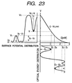
- Fig. 23 is a graph showing the relationship between the distribution of the energy of a light beam, the photosensitive characteristic of a photosensitive body, and the potential distribution on a photosensitive body. As is apparent from Fig. 23, when the photosensitive characteristic of the photosensitive body is linear, the energy distribution of the light beam is directly reflected by the potential distribution on the photosensitive body.
- the step whereat the transferring material P that has passed through the fixing portion is separated from the face of the photosensitive body 1 mainly employs electrostatics, machines, or the curvature of the photosensitive body 1 and the effect of gravity on the transfer material P.
- the transfer material P can be easily separated when the adhesive force between the transferring material P and the photosensitive body 1 is small. This greatly depends on the sealing condition at the portion whereat the transfer material P contacts the photosensitive body 1.
- the adhesive force is especially increased for a smoother transfer material P, such as an OHP sheet, rather than a fiber material, such as paper.
- the step whereat the surface of the photosensitive body 1 is cleaned by the cleaning blade is initiated when the blade closely contacts the surface of the photosensitive body 1 and smoothly slides across the surface.
- the fur brush strikes the hard surface of the photosensitive body 1 directly, and this adverse procedure may be accompanied by the deterioration of the fur brush. Therefore, in this case also, it IS effective for appropriate fogging to be present on the face of the photosensitive body 1.
- the present inventors also found that (4) since, depending on an outward additive or a developing condition, a developer having a small particle diameter can provide greater triboelectricity than a developer having with a particle diameter that contributes to the normal developing, the operability for developing an electrostatic latent image can be changed.
- the present invention is based on this discovery.
- the BAE method is employed for an electrophotographic apparatus, and the half value width Wv of the latent Image potential distribution is reduced relative to the interval between pixels, and a potential gap is formed at the border area between pixels. Further, the containing ratio of a developer having a particle diameter that seldom causes fogging is increased, and high triboelectricity is applied to selectively develop an image. Thus, a developing condition (fogging) that does not adversely affect image quality and the consumption of toner is provided.
- a potential gap is formed at the border area between pixels, and a developer having a particle diameter that seldom causes fogging is selectively attached.
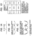
- Fig. 1A there is no substantial fogging.
- Fig. 1D fogging that adversely affects the image quality is not present, but the separation from the photosensitive body property of the transferring material and the cleaning property of the photosensitive body are not good.
- a toner having a particle diameter that will seldom cause fogging that affects image quality is present.
- both cleaning and fogging are established. That is, while the fogging that affects toner consumption and image quality is not increased, the separation of the transferring material from the photosensitive body and/or the cleaning property of the photosensitive body, and/or the life of the cleaning blade or the fur brush can be improved.
- a toner having a particle diameter that affects the image quality by causing a smeared image trailing edge or a fogged image is present.
- the separation property and the cleaning property are good, but naturally fogging occurs that affects image quality.
- One specific mode is an electrophotographic apparatus that radiates a light beam for irradiating individual pixels of a pixel matrix consisting of a plurality of rows and a plurality of columns, and that forms an image using the BAE method.
- A denotes a one-pixel width
- Wv denotes a width at the half value of the peak in the latent image potential distribution that is formed during the irradiation of one pixel using the light beam
- the photosensitive body includes a photosensitive layer containing amorphous silicon, and the containing ratio of a developer having a particle diameter that is equal to or smaller than 1 ⁇ m to the overall developer is 5 to 40 number%.
- the potential between pixels at the border area is not lowered enough.
- fogging that affects the image quality occurs, and when the exposure with light having an increased beam diameter overlaps too much, the line width is reduced.
- the EV property the potential property for the optical energy; the horizontal axis represents the optical energy (E) and the vertical axis represents the potential (V)) of a photosensitive layer is linear, as for a-Si, the potential gap of the light beam irradiation portion, whereat the developer having a particle diameter that seldom causes fogging is developed, can be precisely controlled, and the above described mode can be implemented.
- the containing rate (ratio) of the developer having a particle diameter of 1 to 3 ⁇ m be 2 to 30%.
- the containing ratio is less than 2%, the density of the toner particles that are developed is low, and a smeared image trailing edge tends to occur.
- the containing ratio for the above developer exceeds 30%, fogging is increased in a solid white image.
- the fogging that affects toner consumption and image quality is not increased, and the latitude can be expanded.
- a potential gap is defined at the border area between pixels by defining the above described "5 to 40 number%", and the developer particles having a diameter that seldom causes fogging are selectively developed, fogging that affects toner consumption and image quality is not increased. Further, the separation property and/or the cleaning property, and/or the life of the fur brush can be improved.
- the one-pixel width on the surface of the photosensitive body is equal to or smaller than 80 ⁇ m, the above effects are more apparent.
- the average particle diameter of the developer is 4 to 13 ⁇ m and the containing ratio of the developer having the particle diameter 1 to 3 ⁇ m to the overall developer is 2 to 30 number%, the fogging, the resolution and the smeared image trailing edge are enhanced more.
- a-Si photosensitive layer since no optical energy dependency appears for the potential change of a-Si having the linear EV property relative to the optical energy change, a sharp image can be maintained even when the beam diameter is increased.
- the line width is narrowed and fogging is improved.
- the cleaning property is improved when the amount of fogging becomes equal to or greater than a constant quantity, and this depends on the toner particle diameter and the outward additive (the particle diameter and the quantity).
- the latitude where this relationship has been established is greater for the a-Si photosensitive layer than for the OPC photosensitive layer.
- a preferable combination is "BAE method” + "0.6 ⁇ Wv/A ⁇ 1.0" + "a-Si” + "the above described toner (particle diameter and quantity)".
- the relationship "0.6 ⁇ Wv/A ⁇ 1.0" is established between the one-pixel width A and the width Wv of a latent image, which is formed by projecting a light beam onto one pixel.
- the electrophotographic apparatus can be implemented that has a large design latitude and a high total performance, and the method therefor.
- the width of one pixel on the surface of the photosensitive body is set equal to or smaller than 80 ⁇ m, the above effects are more remarkable.
- the average particle diameter of the developer is set to 4 to 13 ⁇ m and the containing ratio of the developer having the particle diameter 1 to 3 ⁇ m to the overall developer is set to 2 to 30 number%, the fogging, the resolution and the smeared image trailing edge can be improved.
- a fogged toner image is formed on a photosensitive body to provide spacer effects.
- the objective is to provide an image forming apparatus, having an automatic double-sided printing function, that prevents a fixing oil from being transferred to the photosensitive body via a transferring belt or the like, so that the objective differs from that of the present invention.
- the fogged toner forming means of particles having the same polarity as the toner.
- This experiment relates to the control probability for the particle distribution of a developer.
- • styrene-butyl acrylate-butyl maleate half ester copolymer 100 units • magnetic powder 100 units • iron complex of monoazo dye 2 units • low-molecular weight polyethylene 4 units were mixed using a blender, and the mixture was melted and kneaded by using two-axle extruder that was heated to 130°C. The cooled mixture was roughly pulverized using a hammer mill, and then the roughly pulverized material was ground in a pulverizer, such as a jet mill, using a jet stream.
- a pulverizer such as a jet mill
- the obtained powder was strictly classified by a multiple fraction classifier using the Coanda effect, and toner particles were thus obtained.
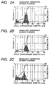
- Fig. 2A The results obtained by measuring the particle distribution of the toner are shown in Fig. 2A.
- the circle corresponding to the diameter was 6 ⁇ m, and one peak was present in an area equal to or smaller than 1 ⁇ m and in an area of 3 to 10 ⁇ m. Further, about 10 number% of particles having a diameter of 1 to 3 ⁇ m were present.
- a surface active agent preferably alkylbenzene sulfonate
- a dispersing agent preferably alkylbenzene sulfonate
- 100 to 150 ml of water in a container, from which solid impurities were removed in advance.
- 0.1 to 0.5 g of a measurement sample was added.
- a dispersion process was performed for the suspension whereby the sample was dispersed using an ultrasonic dispersing device for one to three minutes, and with a dispersion density of 3000 to 10000 number/ ⁇ l, the particles of the developer were measured using the above instrument.
- the pulverization pressure (air pressure) of the pulverizer that employs the jet stream and the feeding volume were adjusted, and/or the air flow rate of the multiple fraction classifier and the position of the division plate were adjusted, and/or the classification step was repeated multiple times.
- the results obtained by preparing the developer having different particle distributions are shown in Fig. 2B and 2C.
- the containing ratios of the particles having a diameter of 3 to 10 ⁇ m, a diameter of 1 ⁇ m or smaller, and a diameter of 1 to 3 ⁇ m can be controlled.
- Fig. 3A is a schematic diagram illustrating the essential portion of an electrophotographic apparatus used for this experiment.
- the electrophotographic apparatus for this experiment is a BAE method laser printer of the reversal development and transfer type (an analog Canon copier NP6750 was improved to obtain a digital copier that includes an optical scanning device).
- Fig. 3B is a diagram showing the arrangement of the optical scanning device (laser scanner).
- a cylindrical (drum) electrophotographic photosensitive body 11 was rotated clockwise at a predetermined peripheral speed, as indicated by an arrow X.
- a main charging device 12, an optical scanning device 13, a developing device 14, a transfer material feeding system 15, a transfer and separation charging device 16, a cleaning device (cleaner) 17, a main charge elimination light source 18, and a conveying system 19 are located near and adjacent to the photosensitive body 11.
- the photosensitive body 11 was uniformly charged to predetermined polarity and potential by the main charging device 12, and the optical scanning device 13 irradiated (scanned and exposed) the charged face using a light beam (image forming beam) L carrying document information. Then, an electrostatic latent image corresponding to the exposure pattern was formed on the photosensitive body 11.
- toner was supplied from the developing device 14, the latent image became a visible image, i.e., a toner image.
- the transferring material P was passed through the transfer material feeding system 15, which included a transfer material path 15a and registration rollers 15b, and was supplied to a gap defined between the photosensitive body 11 and a transferring charging device 16a at a predetermined control timing.
- a transfer material feeding system 15 included a transfer material path 15a and registration rollers 15b
- an electric field having a polarity opposite to that of the toner was applied from the rear, so that the toner image on the surface of the photosensitive body 11 was transferred to the transferring material P.
- a separation charging device 16b the transfer material P was separated from the photosensitive body 11 by charge elimination, was transported by the transfer material conveying system 19, and was discharged to the exterior at a fixing device (not shown).
- the toner that was not used for the transferring process at the transferring portion and that remained on the surface of photosensitive body 11 was delivered to the cleaning device 17 and was removed from the surface of the photosensitive body 11 by a cleaning blade 17a.
- the photosensitive body 11 that was cleaned received charge elimination light from the main charge elimination light source 18, and memory was electrically erased, so that the photosensitive body 11 was again available for the next image forming process.
- the optical scanning device 13 a laser scanner, as is shown in Fig. 3B, included: a laser diode 13a, a rotary polygon mirror 13c and an optical system 13b, for introducing a laser beam emitted by the laser diode 13a to the rotary polygon mirror 13c; and an optical scanning system 13d, for introducing, into the photosensitive body 11, a laser beam L that was deflected by the rotary polygon mirror 13c and for scanning and exposing the photosensitive body 11 using the laser beam L.
- the a-Si photosensitive body was employed for the photosensitive body 11, and an electrostatic latent image of one dot (i.e., no light beam irradiation was performed for only one dot) was formed using the BAE method.
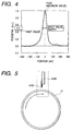
- the results obtained by measuring the electrostatic latent image distribution are shown in Fig. 4.
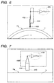
- Figs. 5 to 7 are specific diagrams showing the outline of the latent image distribution method.
- the photosensitive body 11 includes a surface 11a that accompanies a potential change.
- a potential sensor 4103 is supported by a support member 4014 and is connected to a circuit element 4106 by a conducting line 4105.
- Fig. 6 is a partially enlarged diagram for Fig. 5, and Fig. 7 is a schematic diagram for Fig. 6 viewed from the left of the paper.
- the detected induced current included information concerning the inclination of the surface potential.
- the latent image potential distribution could thus be measured by analyzing the included information.
- Fig. 4 the measurement results obtained by the above described latent image distribution measurement method are shown; the horizontal axis represents the position of the latent image on the photosensitive body, and the vertical axis represents the potential of the latent image.
- the half value width (F.W.H.M.) at the one-dot latent image distribution was defined as a latent image width Wv
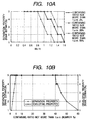
- the rank of the fogging in a solid white image was examined while the ratio of the latent image width Wv to the one-pixel width (the design value of the image forming mechanism) A was changed.
- the obtained results are shown In Fig. 8.
- the relationship between the ratio Wv/A and the slim line image of a line and the relationship between the ratio Wv/A and the slim line image of a dot were examined, and their results are shown in Figs. 9A and 9B.
- This experiment employed a cleanerless (CLNless) printer.
- the printer used for this experiment was so designed that the corona charging device, as the main charging device, of the printer (Figs. 3A and 3B) used for experiment 2 was replaced with a contact charging member, as described in Japanese Patent Application Laid-Open No. 9-43934, and that the transfer/separation charging device 16 was replaced with a transferring roller, while the cleaning device 17 was removed.
- the remainder of the structure of the printer was the same as that used for experiment 2.
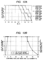
- the separation from the photosensitive body 11 property of the transfer material P was evaluated by changing the ratio of the latent image width Wv to the one-pixel width A.
- This experiment provided representative data relative to the cleaning property (CLN property) of a printer that employed a blade cleaning device 17 (blade CLN), as in the printer in Figs. 3A and 3B.
- a printer (Figs. 3A and 3B) corresponding to the one used in experiment 2 was employed, and the cleaning property was estimated by changing the ratio of the latent image width Wv to the one-pixel width A.
- the cleaning was performed by changing the blade pressure. Warping of the blade was examined by increasing the blade pressure, and cleaning failures, such as the failure to remove developer or chattering, were examined by reducing the blade pressure. Then, an estimate was made for the cleaning property by using a total of five ranks (5 is excellent).
- the estimate for the development property was made by using the same method as was used for experiment 3.
- This experiment concerns the usable life of a fur brush (brushing means) that is used as a cleaning device.
- the printer used for this experiment is the same as the one (Figs. 3A and 3B) used for experiment 2, with the exception that the blade cleaning device 17 was replaced with a fur brush cleaning device.
- a fur brush device was constituted by a support shaft on which a brush was mounted.
- the support shaft was a copper bar with electroless nickel plating, and the outer diameter was 10 mm.
- the brush was made of rayon thread containing carbon, which is sold under the product name "Rec-C" by Unitica Ltd., and was shaped like a cylinder with one end of the thread being securely glued using a conductive adhesive.
- the brush was fixed to the support shaft by double-sided adhesive tape at three places at intervals in the center axial direction.
- the rotary drum was connected via transmission gears to a rotation source, a DC servo motor, and the photosensitive body that was connected to the peripheral surface of the rotary drum was grounded. A cleaning voltage of -250 V was applied to the fur brush.
- the rotary drum was rotated at a peripheral speed of 400 mm/second, and the fur brush was rotated in the opposite direction at a location whereat it contacted the rotary drum.
- the thus arranged printer was employed, and the life of the fur brush was estimated by changing the ratio of the latent image width Wv to the one-pixel width A.
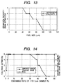
- the printer (Figs. 3A and 3B) used for experiment 2 was employed, the spot diameter of a light beam emitted to irradiate pixels was fixed, the size of a pixel on the photosensitive body was changed, and the separation property of the transfer material P was estimated.
- the printer (Figs. 3A and 3B) used for experiment 2 was employed, the spot diameter of a light beam emitted to irradiate pixels was fixed, the particle distribution of the developer was changed in the same manner as for experiment 1, and a developer was obtained wherein the developer particles having a diameter of 1 to 3 ⁇ m were present at a different ratio (number%).
- the conditions concerning fogging and a image trailing end were estimated, and the obtained results are shown in Fig. 14.
- the potentials at the dark and bright portions of the electrostatic latent image were set to the design values, and a microscope was used to magnify a printed character.
- the condition under which the developing was performed extended from the outline of the character was estimated using a total of five ranks (5 is excellent), while also taking into account the environmental dependency and the endurance.
- the potentials of the dark and bright portions of the electrostatic latent image were set to the design values, the Canon image chart NA-7 was employed, and a microscope was used to magnify a printed image in a resolution pattern (lines/mm). While taking environmental dependency and endurance into account, the resolution was estimated by using a total of five ranks (5 is excellent).
- the printer used for this embodiment was the same cleanerless printer used for experiment 3.
- a main charging device was a contact charging member, and a transfer/separation charging device was a transfer roller.
- the BAE method was employed for image forming, and an a-Si photosensitive body was used.
- the pixel size A was 50 ⁇ m, and the ratio Wv/A of the latent image width Wv to the pixel size A was 0.8.
- a developer having an average particle diameter of 8 ⁇ m was employed wherein particles having a diameter equal to or smaller than 1 ⁇ m were present at a ratio of 20 number% and particles having a diameter of 1 to 3 ⁇ m were present at a ratio of 20 number%.
- Fogging, the line width, the development property, the separation property, the smeared image trailing edge, and the resolution were determined by using ranks of excellent (very good), good, fair (no problem in practical use), and fail (problem in practical use), and the results are shown in Table 1.
- the image forming method, the photosensitive body, the pixel size, the ratio Wv/A, the average particle diameter of the developer, the containing ratio for particles having a diameter of 1 ⁇ m or smaller, and the containing ratio for particles having a diameter of 1 to 3 ⁇ m are the same as those for embodiment 1.
- the image forming method, the photosensitive body, the pixel size, the ratio Wv/A, the average particle diameter of the developer, the containing ratio of particles having a diameter equal to or smaller than 1 ⁇ m, and the particles having a diameter of 1 to 3 ⁇ m were the same as those used for embodiment 1.
- the printer (Figs. 3A and 3B) used for experiment 2 was also used for this embodiment, with the exception that the laser scanner 13, which was an optical scanning, device, was replaced by an optical LED array exposure device.
- the image forming method, the photosensitive body, the pixel size, the ratio Wv/A, the average particle diameter of the developer, the containing ratio of particles having a diameter equal to or smaller than 1 ⁇ m, and the particles having a diameter of 1 to 3 ⁇ m are the same as those for embodiment 1.
- Photosensitive bodies are roughly sorted into an organic type and an inorganic type.
- the function separation photosensitive body has one large problem in that its endurance is generally low.
- the deterioration of the photosensitive body is roughly sorted into electrophotographic deterioration, such as sensitivity, residual potential and charging capability or the occurrence of unfocused images, and mechanical deterioration, such as the abrasion and scratching of the surface of the photosensitive body due to friction. Endurance is a greatly important factor that determines the life of a photosensitive body.
- electrophotographic deterioration especially the occurrence of an unfocused image, results from the deterioration of a charge carrying material, contained in the surface layer of a photosensitive body, that is due to the presence of an active material, such as ozone or NOx, that is generated by the corona charging device.
- an active material such as ozone or NOx
- a charge carrying material to be employed that is not greatly affected by an active material, such as ozone or NOx, and for a charge carrying material having of a high oxide potential to be selected.
- a slip additive such as fluorocarbon polymer powder, graphite fluoride powder, or polyolefin polymer powder, can be mixed into the surface layer.
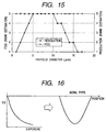
- an organic photosensitive body generally has a field dependency derived from the principle of carrier transmission. Since the EV property (the potential property related to optical energy; the horizontal axis representing the optical energy and the vertical axis representing the potential) has a downward projected shape, as is shown in Fig. 16, a small optical energy change tends to be reflected in the potential.
- the EV property the potential property related to optical energy; the horizontal axis representing the optical energy and the vertical axis representing the potential
- a small optical energy change tends to be reflected in the potential.
- a photoconductor material having such an superior property is, for example, amorphous silicon hydride (hereinafter referred to as "a-Si:H”), and in Japanese Patent Publication No. 60-35059, this material is used for a photosensitive body for an image forming apparatus.
- a-Si:H amorphous silicon hydride
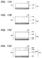
- Figs. 17A to 17D are specific diagrams for explaining the layer structure of a photosensitive body.
- a photosensitive body 1100 in Fig. 17A is designed so that a photosensitive layer 1102 is deposited on a support body 1101.
- the photosensitive layer 1102 includes a photoconductive layer 1103 composed of a-Si:H,X.
- a photosensitive body 1100 in Fig. 17B is so designed that a photosensitive layer 1102 is deposited on a support body 1101.
- the photosensitive layer 1102 includes a photoconductive layer 1103 composed of a-Si:H,X, and an amorphous silicon surface layer 1104.
- a photosensitive body 1100 in Fig. 17C is so designed that a photosensitive layer 1102 is deposited on a support body 1101.
- the photosensitive layer 1102 includes a photoconductive layer 1103 composed of a-Si:H,X, an amorphous silicon surface layer 1104, and an amorphous silicon charge injection prevention layer 1105.
- a photosensitive body 1100 in Fig. 17D is so designed that a photosensitive layer 1102 is deposited on a support body 1101.
- the photosensitive layer 1102 includes a charge generation layer 1106, composed of a-Si:H,X, and a charge carrying layer 1107, both of which consist of a photoconductive layer 1103, and an amorphous silicon surface layer 1104.
- the conductive support body is heated to 50 to 400°C, and a photoconductive layer made of a-Si is formed on the support body using a film deposition method, such as vacuum evaporation, sputtering, ion plating, thermal CVD, optical CVD or plasma CVD (hereinafter referred to as "PCVD").
- a film deposition method such as vacuum evaporation, sputtering, ion plating, thermal CVD, optical CVD or plasma CVD (hereinafter referred to as "PCVD").
- PCVD plasma CVD
- a photosensitive body for an image forming apparatus, that includes a conductive support body and an a-Si (hereinafter referred to as "a-Si:X”) photoconductive layer that contains halogen atoms as components.
- a-Si:X a-Si
- halogen atoms when halogen atoms are contained in a-Si at 1 to 40 atomic %, high heat resistance and satisfactory electric and optical properties can be obtained by the photoconductor layer of a photosensitive body used for an image forming apparatus.
- a technique whereby a surface layer composed of a non-photoconductive amorphous material that contains silicon atoms and carbon atoms is deposited on a photoconductive layer made of an amorphous material that mainly contains silicon atoms, in order to improve the electric, optical and photoconductive properties of the photoconductive member, including the photoconductive a-Si film, such as a dark resistance value, photosensitivity and optical responsibility, a use environment property, such as moisture resistance, and time-transient stability.
- Japanese Patent Application Laid-Open No. 60-67951 a technique is disclosed for a photosensitive body on which is laminated a light transmitting and insulating overcoating layer containing amorphous silicon, carbon, oxide and fluorine.
- a technique is disclosed that employs, for a surface layer, a non-amorphous material containing silicon atoms, carbon atoms and hydrogen atoms at 41 to 70 atomic %.
- a photoconductor layer is formed of a-Si:H, wherein hydrogen at 10 to 40 atomic % is contained and for which the absorption coefficient ratio for the infrared absorption spectrum, at absorption peaks of 2100 cm -1 and 2000 cm -1 , is 0.2 to 1.7.
- a sensitive and highly resistant photosensitive body can be obtained for an image forming apparatus.
- the electric, optical and photoconductive properties of a photosensitive body used for an image forming apparatus, and environmental property use are enhanced, while the image quality is also improved.
- sensitivity it is general rule that an amorphous photosensitive body does not have field dependency in accordance with the principle of carrier transmission, and that the EV property has a linear shape, as is shown in Fig. 18, so that an optical energy change is not reflected by the potential.
- the optical energy distribution and the potential distribution are both Gaussian distributions. So that when the bottom of the optical distribution is changed, the dot diameter is comparatively little affected, and image quality is seldom deteriorated.
- the support body 1101 may be either conducive or insulating.
- a conductive support body 1101 can be made of a well known metal, such as Al or Fe, or an alloy of these metals, such as stainless steel.
- an insulating support body 1101 can be made of a synthetic resin film or sheet (glass or a ceramic may also be employed) for which the conduction process has at least been performed on the surface on which a photosensitive layer is to be formed.
- the shape of the support body 1101 may be a cylinder, a plate, or an endless belt having a smooth surface or a raised or recessed surface.
- the surface of a support body 1101 may be raised or recessed so long as the charge carriers are not substantially reduced, and an image failure due to a so-called coherent striped pattern that appears on a visible image can be effectively avoided.
- a well known method disclosed in Japanese Patent Application Laid-Open Nos. 60-168156, 60-178457 and 60-225854 can be employed.
- multiple spheroidal trace dents may be formed to raise or recess the surface of a support body 1101 so long as the charge carriers are not substantially reduced. That is, the surface of a support body 1101 may have raised and recessed portions exceeding the resolution that is requested of the photosensitive body 1100, and these raised and recessed portions can be formed by using multiple spheroidal trace dents.
- the method disclosed in Japanese Patent Application Laid-Open No. 61-231561 is employed to form multiple spheroidal trace dents to raise and recess the surface of a support body 1101.
- an interference prevention layer or area such as a light absorption layer, may be formed inside or under the photosensitive layer 1102.
- the photosensitive layer 1103 that constitutes one part of the photosensitive layer 1102 is deposited on an underlayer (not shown) that is formed as needed on a support body 1101. Before the photoconductive layer 1103 is formed by vacuum film deposition, an appropriate numerical condition for a deposition parameter is set in order to obtain a desired property.
- various thin film deposition methods can be employed; for example, the glow discharge method (an alternating-current discharge CVD, such as a low frequency CVD, a high frequency CVD or a microwave CVD, or a direct-current discharge CVD), sputtering, vacuum evaporation, ion plating, optical CVD and thermal CVD.
- the glow discharge method an alternating-current discharge CVD, such as a low frequency CVD, a high frequency CVD or a microwave CVD, or a direct-current discharge CVD
- sputtering vacuum evaporation, ion plating
- optical CVD optical CVD
- thermal CVD thermal CVD
- These thin-film deposition methods are selected in accordance with manufacturing conditions, equipment investment overheads, manufacturing scale and the properties desired for the photosensitive body that is to be produced.
- the glow discharge method is most appropriate because the conditions for manufacturing a photosensitive body having desired properties are comparatively easy to control.
- a material gas for supplying silicon atoms (Si) and a material gas for supplying hydrogen atoms (H), and/or a material gas for supplying halogen atoms (X) are introduced in desired states into a reaction container for which the pressure can be reduced. Then, the glow discharge is initiated inside the reaction container, and only a layer composed of a-Si:H,X need be deposited on the support body 1101 that is positioned at a predetermined location in advance.
- the photoconductive layer 1103 It is necessary for the photoconductive layer 1103 to contain hydrogen atoms and/or halogen atoms, in order to compensate for non-bonding portions of silicon atoms, and to improve the layer quality, especially, the photoconductive and charge holding properties. Therefore, preferably, the content of hydrogen atoms or halogen atoms, or the sum of the hydrogen atoms and the halogen atoms is 10 to 30 atomic %, or more preferably, 15 to 25 atomic %, relative to the sum of the silicon atoms and hydrogen atoms and/or the halogen atoms.
- Silicon hydride (silan) in a gaseous state, or in a state that can be gasified, is effectively employed as the material for an Si supply gas.
- SiH 4 and Si 2 H 6 are especially preferable because they are easy to handle during the layer deposition process, and the efficiency with which Si is supplied is superior.
- a silicon compound gas containing H 2 and/or He or hydrogen atoms it is also necessary for a desired amount of a silicon compound gas containing H 2 and/or He or hydrogen atoms to be mixed with the above gas in order to form a layer.
- hydrogen atoms can be systematically introduced into the photosensitive layer 1103, the ratio of the hydrogen atoms to be introduced can be more easily controlled, and the film property that implements the purpose of the process can be obtained.
- a plurality of gases may be mixed at a predetermined mixture ratio.
- an effective material gas for supplying halogen atoms is a halogen gas, or a halogen compound, such as halide, an inter-halogen compound containing halogen or a silan derivative that is replaced by halogen, that is in the gaseous state or that can be gasified.
- a silicon hydride compound that contains silicon atoms and halogen atoms and that is in a gaseous state or that can be gasificated can be effective.
- atoms that control conduction be contained, as needed, in the photoconductive layer 1103.
- the atoms that control the conduction may be uniformly contained in the photoconductive layer 1103, or may be partially contained with an uneven distribution extending in the direction of the thickness of the layer.
- a so-called impurity in a semiconductor field can be employed as the atoms for controlling the conduction.
- such atoms can be those (the IIIb atoms) that belong to the IIIb group in the periodic table for providing the p-type conductive property, or those (the Vb atoms) that belong to the Vb group in the periodic table for providing the n-type conductive property.
- the material that is used for introducing the atoms that control the conduction may be diluted with H 2 and/or He.
- carbon atoms and/or oxygen atoms, and/or nitrogen atoms it is also effective for carbon atoms and/or oxygen atoms, and/or nitrogen atoms to be contained in the photoconductive layer 1103.
- the carbon atoms and/or the oxygen atoms, and/or the nitrogen atoms may be uniformly contained in the photoconductive layer 1103, or may be contained in one part extending in the direction of the thickness of the layer 1103 with an uneven distribution that provides for the changing of the content.
- the desired thickness of the photoconductive layer 1103 is determined while taking into account a desired electrophotographic property and economic effects.
- the thickness of the photoconductive layer 1103 is 20 to 50 ⁇ m, or more preferably, 23 to 45 ⁇ m, or optimally, 25 to 40 ⁇ m.
- the mixture ratios for the Si supply gas and the diluted gas, the gas pressure in the reaction container, the discharge power and the temperature of the support body can be appropriately determined.
- the above described conditions are not determined independently, and it is preferable that optimal values for them be determined based on mutual and organic relationships in order to acquire a photosensitive body having desired properties.
- the surface layer 1104 be formed on the photoconductive layer 1103 that is deposited on the support body 1101 in the above described manner.
- the surface layer 1104 has a free surface 1106, and is deposited mainly to provide humidity resistance, a property for continuous and repetitive employment, pressure resistance, a usage environmental property and endurance.
- the surface layer 1104 is preferably made of amorphous silicon (a-Si); amorphous silicon (hereinafter referred to as "a-SiC:H,X”) that contains hydrogen atoms (H) and/or halogen atoms (X) and carbon atoms; amorphous silicon (hereinafter referred to as "a-SiO:H,X”) that contains hydrogen atoms (H) and/or halogen atoms (X) and oxygen atoms; amorphous silicon (hereinafter referred to as "a-SiN:H,X”) that contains hydrogen atoms (H) and/or halogen atoms (X) and nitrogen atoms; or amorphous silicon (hereinafter referred to as "a-SiCON:H,X”) that contains hydrogen atoms (H) and/or halogen atoms (X) and further contains at least either carbon atoms, oxygen atoms or nitrogen atoms.
- a-SiC:H,X
- the surface layer 1104 is formed by the vacuum film deposition method while an appropriate numerical condition for a film deposition parameter is set to obtain a desired property.
- various thin film deposition methods can be employed; for example, the glow discharge method (an alternating-current discharge CVD, such as the low frequency CVD, the high frequency CVD or the microwave CVD, or a direct-current discharge CVD), sputtering, vacuum evaporation, ion plating, optical CVD and thermal CVD.
- glow discharge method an alternating-current discharge CVD, such as the low frequency CVD, the high frequency CVD or the microwave CVD, or a direct-current discharge CVD
- sputtering vacuum evaporation, ion plating
- optical CVD optical CVD
- thermal CVD thermal CVD
- a material gas for supplying silicon atoms (Si), a material gas for supplying carbon atoms (C), and a material gas for supplying hydrogen atoms (H) and/or a material gas for supplying halogen atoms (X) are introduced in desired states into a reaction container for which the pressure can be reduced. Then, the glow discharge is initiated inside the reaction container, and only a layer composed of a-SiC:H,X need be deposited on the photoconductive layer 1103 that is formed on the support body 1101 is positioned at a predetermined location.
- the carbon content fall within the range of 30 to 90% of the sum of the silicon atoms and the carbon atoms.
- the surface layer 1104 It is also necessary for the surface layer 1104 to contain hydrogen atoms and/or halogen atoms, in order to compensate for non-bonding portions of silicon atoms, and to improve the layer quality, especially the photoconductive and charge holding properties. Therefore, the content of hydrogen atoms, relative to the total of the constituent atoms, is normally 30 to 70 atomic %, preferably, 35 to 65 atomic %, and optimally, 40 to 60 atomic %.
- the content of the fluorine atoms is normally 0.01 to 15 atomic %, preferably, 0.1 to 10 atomic %, and optimally 0.6 to 4 atomic %.
- a defect in the surface layer (mainly a dangling bond of the silicon atoms and carbon atoms) adversely affects the properties of a photosensitive body used for an image forming apparatus.
- the charging property is deteriorated by the injection of electric charges from the free surface into the photoconductive layer; the charging property is caused to fluctuate by changing the surface structure in accordance with the employment environment, e.g., at a high humidity; or an afterglow phenomenon occurs during repetitive employment while corona charging or light irradiation is being performed, or when electric charges from the photoconductive layer are injected into the surface layer and are trapped in a defect therein.
- the content of hydrogen in the surface layer is adjusted to a ratio that is equal to or greater than 30 atomic %, defects in the surface layer are is considerably reduced, and electric properties and fast continuous usage can be improved.
- the content of hydrogen in the surface layer exceeds 70 atomic %, the hardness of the surface layer is reduced, and endurance is deteriorated.
- one action performed by the fluorine atoms in the surface layer is the effective prevention of the separation, due to damage, of the silicon atoms and the carbon atoms, such as is induced by a corona discharge.
- the content of fluorine in the surface layer exceeds 15 atomic %, there is substantially no effect on the bonding of the silicon atoms and the carbon atoms in the surface layer, but the separation of bonded atoms is prevented. Further, since excessive fluorine atoms disturb the movement of the carrier in the surface layer, the residual potential and the image memory are remarkable.
- the fluorine content and the hydrogen content of the surface layer can be controlled by the flow rate of the H 2 gas, the temperature of the support body, the discharge power, and the gas pressure.
- the thickness of the surface layer 1104 is normally 0.01 to 3 ⁇ m, preferably, 0.05 to 2 ⁇ m, and optimally, 0.1 to 1 ⁇ m.
- the thickness of the surface layer is less than 0.01 ⁇ m, the surface layer is lost due to abrasion while the photosensitive body is in use. And when the thickness of the surface layer exceeds 3 ⁇ m, deterioration of electrophotographic properties, such as an increase in the residual potential, occurs.
- the surface layer 1104 is formed carefully so as to obtain a desired property as requested. That is, the material that contains Si, C and/or N and/or O, H and/or X can employ the crystal structure or the amorphous structure in accordance with the deposition condition. Further, the conductive property, the semiconductive property or the insulating property is employed as the electric property, and either the photoconductive property or the non-photoconductive property is employed. Thus, the formation condition is strictly selected so as to obtain a compound having a desired property that is consonant with the objective.
- the surface layer 1104 is formed as a non-amorphous member whose insulating property is remarkable in the usage environment.
- the surface layer 1104 is formed as a non-amorphous member whose insulating property is moderate to a degree and that is sensitive to a degree to a projected light.
- the surface layer 1104 it is preferable that, during the deposition of the surface layer 1104, its resistance be appropriately controlled in order to prevent image smearing due to low resistance of the surface layer 1104 or to prevent an adverse effect stemming from the residual potential, and to enhance the charging efficiency.
- a blocking layer which contains fewer carbon atoms, oxygen atoms and nitrogen atoms than the surface layer, to be deposited between the photoconductive layer and the surface layer, so as to further enhance the charging capability.
- an area wherein the content of the carbon atoms and/or oxygen atoms and/or the nitrogen atoms is reduced toward the photoconductive layer 1103 may be provided between the surface layer 1104 and the photoconductive layer 1103.
- the surface layer 1104 and the photoconductive layer 1103 can contact each other more closely, and the affect of the interference due to the reflection of light on the surface can be further reduced.
- amorphous carbon (a-C) It is also effective for amorphous carbon (a-C) to be employed for the surface layer 1104.
- the a-C material has the same of greater hardness as does the a-SiC, and is superior in water repellency, endurance and printing resistance.
- the a-C surface layer is used as a part or as all of the surface layer 1104, the printing resistance property and the environmental property can be further improved.
- the charge injection prevention layer 1105 it is more effective for the photosensitive body of the image forming apparatus for the charge injection prevention layer 1105 to be formed between the support body and the photoconductive layer since it can prevent the injection of charges from the support body.
- the charging injection prevention layer functions to prevent charges from the support body from being injected into the photoconductive layer. But when the charge on the free surface of the photosensitive layer has the opposite polarity, the above function is not performed. In other words, the charge injection prevention layer has a so-called polarity dependency. To obtain such a function, a greater number of atoms that control the conduction are contained in the charge injection prevention layer than in the photoconductive layer.
- the atoms that control the conduction may be uniformly distributed in the layer, or may partially be distributed non-uniformly while they are arranged evenly in the direction of the thickness of the layer. When the distribution density is uneven, preferably more of these atoms are distributed near the support body.
- impurities in the semiconductor field can be employed as the atoms that are contained in the charge injection prevention layer 1105 to control conduction.
- Such impurities can be atoms that belong to the III group in the periodic table, for providing the p-type conductive property, or atoms that belong to the V group in the periodic table, for providing the n-type conductive property.
- the atom content in the charge injection prevention layer required for controlling conduction can be appropriately determined so as to effectively achieve that objective.
- the carbon atoms, the nitrogen atoms or the oxygen atoms may be uniformly distributed in the layer, or they may partially be distributed non-uniformly while they are evenly arranged toward the thickness of the layer. In either case, however, it is necessary for the atoms to be arranged evenly with a uniform distribution extending toward the surface of the support body and toward the parallel planes, so that along the planes a uniform property is obtained.
- the carbon atoms and/or nitrogen atoms and/or oxygen atoms that are contained in the charge injection prevention layer 1105 can be appropriately determined so as to effectively achieve that objective.
- the hydrogen atoms and/or halogen atoms that are contained in the charge injection prevention layer can effectively compensate for the non-bonding portions present in the layer and thus enhance the film quality.
- the thickness of the charge injection prevention layer is preferably 0.1 to 5 ⁇ m, more preferably, 0.3 to 4 ⁇ m, and optimally, 0.5 to 3 ⁇ m.
- the same vacuum deposition method used for forming the photoconductive layer is also employed to form the charge injection prevention layer 1105.
- an area wherein, at the least, aluminum atoms, silicon atoms and hydrogen atoms and/or halogen atoms are distributed evenly toward the thickness of the layer be provided near the support body 1101 of the photosensitive layer 1102.
- a close contact layer may be formed of an amorphous material that employs, as its primary element, Si 3 N 4 , SiO 2 , SiO or silicon atoms, and that contains hydrogen atoms and/or halogen atoms, and carbon atoms and/or oxygen atoms and/or nitrogen atoms, so that the contact between the support body 1101 and the photoconductive layer 1103 or the charge injection prevention layer 1105 is further improved.
- a light absorption layer may be formed to prevent the occurrence of a coherent pattern due to the light reflected by the support body.
- Fig. 19 is a diagram showing an example apparatus that performs the high frequency plasma CVD method (hereafter referred to as the "RF-PCVD") that employs a RF band.
- RF-PCVD the high frequency plasma CVD method
- This apparatus comprises a deposition device 2100, a material gas supplying device 2200, and an air exhaust device (not shown) for reducing the pressure in a reaction container 2111.
- a cylindrical support body 2112, a support body heater 2113 and a material gas introduction pipe 2114 are located in the reaction container 2111 of the deposition device 2100, and a high frequency matching box 2115 is connected to the reaction container 2111.
- the material gas supply device 2200 includes cylinders 2221 to 2226 for material gases, such as SiH 4 , H 2 , CH 4 , B 2 H 6 and PH 3 ; corresponding valves 2231 to 2236, 2241 to 2246 and 2251 to 2256; and mass flow controllers 2211 to 2216.
- the cylinders containing the individual material gases are connected via a valve 2260 to the gas introduction pipe 2114 of the reaction container 2111.
- Fig. 20 is a diagram showing an example apparatus that performs the high frequency plasma CVD method (hereinafter referred to as the "VHF-PCVD") using the VHF band.
- VHF-PCVD the high frequency plasma CVD method
- This manufacturing apparatus which uses the VHF-PCVD method, Is so designed that the deposition device 2100 in Fig. 19 is replaced with a deposition device 3100 in Fig. 20, and the deposition device 3100 is connected to the material gas supply device 2200.
- this apparatus comprises: a reaction container 3111 having a airtight vacuum structure, wherein the pressure can be reduced; the material gas supplying device 2200 (Fig. 19); and an air exhaust device (not shown) for reducing the pressure in the reaction container 3111.
- a cylindrical support body 3112, a support body heater 3113, a material gas introduction pipe 3114 and an electrode are located inside the reaction container 3111, and a high frequency matching box 3120 is connected to the electrode. Further, the reaction container 3111 is connected to a diffusion pump (not shown) via an air exhaust pipe 3112, and a space 3130 enclosed by the cylindrical support body 3112 serves as a discharge space.
- the amorphous photosensitive body does not have a field dependency and the EV property has a linear shape, as is shown in Fig. 18, so that an optical energy change is not easily reflected onto the potential. Therefore, the optical energy distribution and the potential distribution are both Gaussian distributions. Thus, when the bottom of the optical distribution is changed, the size of the dot diameter is comparatively little affected, and the image quality is seldom deteriorated. In addition, since abrasion due to endurance is not required, the change in the sensitivity, i.e., the endurance change of the EV property, is small, and a problem that has arisen for the OPC that is associated with abrasion does not occur.
- the developer mainly consists of resin particles that contain a coloring agent and an outward additive, and preferably, the outward additive consists of fine inorganic particles.
- the fine inorganic particles are employed for the outward additive because these particles are not easily affected by the environment, and do not deteriorate the flowability of toner, even at a high temperature and a high humidity, so that the preservative property of the toner is not degraded.
- black coloring agent carbon black, magnetic powder, and the yellow, magenta and cyan coloring agents listed below are employed to adjust the color to obtain black.
- a condensed azo compound for a yellow coloring agent, a condensed azo compound, an iso-indolinone compound, an anthraquione compound, an azo metal complex, a methine compound or an allyl amido compound is employed.
- C.I. pigment yellow 12, 13, 14, 15, 17, 62, 74, 83, 93, 94, 95, 97, 109, 110, 111, 120, 127, 128, 129, 147, 168, 174, 176, 180, 181 or 191 is preferably employed.
- magenta coloring agent For a magenta coloring agent, a condensed azo compound, a diketopyrrolopyrrole compound, an anthraquione compound, a quinacridon compound, a basic dye lake compound, a naphthol compound, a benzimidazolone compound, a thioindigo compound or a perylene compound is employed.
- C.I. pigment red 2, 3, 5, 6, 7, 23, 48:2, 48:3, 48:4, 57:1, 81:1, 144, 146, 166, 169, 177, 184, 185, 202, 206, 220, 221 or 254 is particularly preferable.
- a cyan coloring agent for a cyan coloring agent, a copper phthalocyanine compound and its derivative, an anthraquione compound, or a basic dye lake compound can be employed.
- C.I. pigment blue-1, 7, 15, 15:1, 15:2, 15:3, 15:4, 60, 62 and 66 can be preferably employed.
- coloring agents can be used independently or can be mixed, or can be used as a solid solution.
- a coloring agent is selected while taking into account the color phase angle, the color saturation, the brightness, the weather resistance, the OHP transmission property, and the property for dispersion through the toner.
- 1 to 20 parts of coloring agent by mass are added to 100 parts of resin by mass.
- the magnetic powder is a metal oxide including elements, for example, of iron, cobalt, nickel, copper, magnesium, manganese, aluminum or silicon.
- a metal oxide in which iron oxide, such as triiron tetroxide or ⁇ -iron oxide, is contained is especially preferable as the primary element.
- metal elements such as silicon elements or aluminum elements, may be included.
- the BET specific surface area measurement acquired using the nitrogen absorption method is preferably 2 to 3 m 2 /g, with 3 to 28 m 2 /g being particularly preferable, and the Mohs' hardness is preferably 5 to 7.
- the magnetic powder can be shaped like an octahedron, a hexahedron, a spheroid, a needle or a scale; however, an octahedron, a hexahedron, a spheroid or a less anisotropic, indeterminate shape is preferable and increases image density.
- the average particle diameter of the magnetic powder is preferably 0.05 to 1.0 ⁇ m, more preferably, 0.1 to 0.6 ⁇ m, and optimally, 0.1 to 0.4 ⁇ m.
- the amount of magnetic powder contained in 100 parts by mass of binder resin is preferably 30 to 200 parts by mass, more preferably, 40 to 200 parts by mass, and optimally 50 to 150 parts by mass.
- the magnetic powder is less than 30 parts by mass, the toner carrying property is insufficient for a developing device that employs magnetic force to carry toner, and an uneven image will tend to be generated on the developer layer on the developer carrying body. Further, the image density tends to be reduced due to the rise in triboelectricity in the developer.
- the magnetic powder exceeds 200 parts by mass, a fixing property problem arises.
- a well known outward additive can be employed, however, to improve the charging stability, the developing property, the flowability and the preservative property.
- an inorganic fine powder such as silica, alumina or titania, or a double oxide thereof is preferable, and silica is even more preferable.
- the silica can be either dry silica or so-called fumed silica, which is generated by performing a drying process for vapor phase oxidization of a halogen silicon compound or alkoxide, or so-called wet silica, which is produced from alkoxide and water glass.
- Dry silica is more preferable because only a small amount of the silanol group is present on the surface and in the fine silica powder, and after production, there is little Na 2 O or SO 3 2- residue remaining.
- a metal halogen compound such as aluminum chloride or titanium chloride
- a silicon halogen compound during the production process, a composite powder consisting of the dry silica and the other metal oxide can be obtained. This magnetic powder is also included for the outward additive.
- Satisfactory results can be obtained by using a fine inorganic powder for which the BET specific surface area measurement acquired using the nitrogen absorption method falls 30 m 2 /g or more, specifically, 50 to 400 m 2 /g.
- the fine silica powder of 0.1 to 8 parts by mass, but preferably, 0.5 to 5 parts by mass, or more preferably, 1.0 up to 3.0 parts by mass, should be added to 100 parts by mass of the toner.
- the fine inorganic powder be processed, as needed, by a treating agent, such as silicone varnish, silicone oil, various types of degenerated silicone oil, a silan coupling agent, a silan coupling agent including a functional group, another organic silicon compound or an organic titanium compound, or by a combination of these treating agents.
- a treating agent such as silicone varnish, silicone oil, various types of degenerated silicone oil, a silan coupling agent, a silan coupling agent including a functional group, another organic silicon compound or an organic titanium compound, or by a combination of these treating agents.
- the specific surface area measurement device Autosoap 1 (Yuasa Ionics Co., Ltd.) was employed to attach the nitrogen gas to the surface of a sample, and the specific surface area was calculated using the BET multi-point method.
- the fine inorganic powder at least be treated using silicon oil.
- An outward additive other than fine silica powder, may be added to the magnetic toner, as needed.
- Such an outward additive is, for example, fine resin powder or fine inorganic powder that serves as an auxiliary charging agent, a conductivity applying agent, a flowability applying agent, a caking prevention agent, a releasing agent for the fixing process using a thermal roll, a slip additive, or an abrasive.
- a polymerized monomer that is used to form the resin is: a styrene monomer, such as styrene, o-methylstyrene, m-methylstyrene, p-methylstyrene, p-methoxystyrene or p-ethylstyrene; methacrylic acids, such as acrylate and methacrylate; an acrylic ester, such as methylacrylate, ethylacrylate, n-butylacrylate, isobutylacrylate, n-propyl acrylate, n-octyl acrylate, dodecylacrylate, 2-ethylhexyl acrylate, stearylacrylate, 2-chlorethyl acrylate or phenylacrylate; a methacrylic ester, such as methylmethacrylate, e
- Suspension polymerization, emulsion polymerization, or soap free polymerization can be employed as the polymerization method; however, particles obtained using soap free polymerization are preferable.
- fine resin powder that has the above feature provides particularly great effects during drum fusion performed for a contact charging system, such as a roller, a brush or a blade, that serves as the primary charging device.
- a slip additive such as Teflon, zinc stearate or polyvinyliden fluoride, is preferable, with polyvinyliden fluoride being especially preferable.
- an abrasive such as cerium oxide, silicon carbide or strontium titanate, is preferable, with strontium titanate being particularly preferable.
- a flowability applying agent such as titanium oxide or aluminum oxide is preferable, with a hydrophobic agent being particularly preferable.
- a small amount of a caking prevention agent, conductivity applying agent, such as carbon black, zinc oxide, antimony oxide or tin oxide, or a fine white powder or a fine black powder having the opposite polarity can be employed as a development enhancing agent.
- the charge control agent may be mixed with toner particles, or may be added to toner particles.
- the optimal charge control can be exercised in accordance with the developing system, and particularly in this invention, the balance between particle distribution and charge quantities can be further stabilized.
- the following material is used to maintain a toner having a negative charge.
- An organic metal complex or a chelate compound for example, is effective, as is a metal complex such as, for example, a monoazo metal complex, an acetylacetone metal complex, or a metal complex of aromatic hydroxycarboxylic acid or aromatic dicarbonic acid.
- a metal complex such as, for example, a monoazo metal complex, an acetylacetone metal complex, or a metal complex of aromatic hydroxycarboxylic acid or aromatic dicarbonic acid.
- the following materials can be used independently, or a combination of two or more can be used to maintain a toner having a positive charge:
- the above charge control agent be used as fine powder.
- the average particle diameter of the charge control agent should be equal to or smaller than 4 ⁇ m, and preferably equal to or smaller than 3 ⁇ m.
- toner As one example preferable method, a pigment, a dye or magnetic powder that is used as a binder resin or a coloring agent, wax if necessary, a metallic salt or a metal complex, a charge control agent and other additives are mixed together in a mixer, such as a henshel mixer or a ball mill. The obtained mixture is then melted and kneaded using a heat kneader, such as a heat roll or an extruder. Then, a coloring agent and, as needed, a metal compound, a pigment or a dye are dispersed or melted into the resins that have now been rendered compatible, and the resultant mixture is solidified by cooling and is thereafter pulverized. Following this, the classification and surface process is performed as needed to obtain toner particles. Thereafter, inorganic fine powder is added as needed, and finally the toner is obtained.
- a mixer such as a henshel mixer or a ball mill.
- the obtained mixture is then melted and kneaded using
- the mixture may be merely pulverized (and classified as needed) by a well known pulverizer, such as a mechanical impact or a jet pulverizer.
- a well known pulverizer such as a mechanical impact or a jet pulverizer.
- the resin mixture be pulverized by heating, and further that mechanical impact be applied to the resultant material.
- a method for dispersing the fine toner particles that have been pulverized (and classified as needed) in hot water, or a method for passing the toner particles through a hot air stream may be employed.
- the method for performing a process using mechanical impact is the most preferable when taking into account the reduction in the charges held by the toner, the transfer property and the other image properties, and the productivity.
- the means for applying mechanical impact is, for example, a method for which is used a mechanical impact type pulverizer, such as a cryptoron system produced by Kawasaki Heavy Industries, Ltd. or a turbo mill produced by Turbo Industries, Ltd., or a method for using an apparatus, such as a mechanofusion system produced by Hosokawa Micron Co., Ltd. or a hybridization system produced by Nara Machinery Co., Ltd., that employs the centrifugal force of a rapidly rotating blade to push toner inside a casing, and that exerts mechanical impact on the toner by using compression and friction.
- a mechanical impact type apparatus produced by Turbo Industries, Ltd.
- Japanese Patent Publication No. 42-27021 see Fig.
- the rotor 114 is rotated in an atmosphere of 35°C or higher at a peripheral blade 121 speed of 60 to 150 m/sec, and the circular distribution and the particle distribution are adjusted while the toner is pulverized.
- a surface process is performed during which mechanical impact is applied.
- the process for exerting the mechanical impact be performed after the toner pulverization process, or after the succeeding classification process, because the occurrence of a smearing image trailing edge is prevented and the preservative property of the toner is improved.
- Either the classification process or the surface process may be performed first, and it is preferable that the multi-fraction classification device be employed for the classification process to improve the production efficiency.
- a fur brush member which is the cleaning element used for a fur brush cleaning device, is generally formed of: an assemblage of fibers wherein a resin, such as rayon, nylon, acryl, polyester or polyimido, is employed as the main element and hydrotalcite (Mg 2 Al 2 (OH) 16 CO 3 ⁇ 4H 2 O) is mixed in as needed; an assemblage of fibers wherein a resin, such as rayon, nylon, acryl, polyester or polyimido, is employed as the main element, and carbon particles, metal powder or a phenol resin are carbonated; or an assemblage of artificial conductive fibers wherein a conductive material, such as a stainless fiber, is dispersed and the hydrator is mixed as needed.
- a resin such as rayon, nylon, acryl, polyester or polyimido
- hydrotalcite Mg 2 Al 2 (OH) 16 CO 3 ⁇ 4H 2 O
- the artificial fiber is obtained by extracting, through nozzles, a resin liquid in which an appropriate amount of carbon particles are dispersed.
- the conducive fiber may be grounded or a direct current bias may be applied to it.
- the volume resistance of the artificial fiber can be arbitrarily selected by changing the amount of dispersed carbon particles.
- the thickness and the shape in cross section of the artificial fiber can be changed as needed in accordance with the diameter and the shape of the nozzle.
- An appropriate fiber is 3 to 50 deniers (0.33 ⁇ 10 -6 to 5.56 ⁇ 10 -6 kg/m), and an appropriate density is 40000 to 100000/inch 2 (25.8 to 65.4/m 2 ).
- a cylindrical brush is formed of these fibers with one end of each fiber being securely glued using a conducive adhesive, and wound around a support shaft prepared by plating a copper bar.
- the fiber be one that is easily charged to the negative polarity, such as urethane resin, silicon resin, polyester resin fluorine resin (e.g., Teflon resin), or polyimido resin.
- the brush material be one that is easily changed to the positive polarity, such as urethane resin, polyamide or nylon.
- the fiber contain a metal oxide, such as silica, alumina, titania, tin oxide, zirconia or zinc oxide, carbon black, and the charge control agent that is generally used for the developer.
- a metal oxide such as silica, alumina, titania, tin oxide, zirconia or zinc oxide, carbon black, and the charge control agent that is generally used for the developer.
- a fiber mixed with a powdered inter-layer compound such as hydrogencarbonate mineral, having a Moh's hardness (10 levels) of 1.5 to 3.0 and Ph 8.0 to 10.0, is employed for the fur brush.
- a powdered inter-layer compound such as hydrogencarbonate mineral, having a Moh's hardness (10 levels) of 1.5 to 3.0 and Ph 8.0 to 10.0.
- the inter-layer compound performs an anionic exchange between nitric ions and carbonic ions, so that the nitric ions are rendered harmless and smearing of an image is eliminated.
- the anionic exchange fiber is employed for the fur brush; however, there is no description of the effects provided for an a-C:H,X surface layer and the effects inherent to the inter-layer compound (hydrotalcite).
- the present invention provides an electrophotographic apparatus which has a photosensitive body, electrostatic image forming device for forming an electrostatic image on the photosensitive body, the electrostatic image forming device including exposing device for exposing the photosensitive body by a digital light in accordance with image information, and the exposing device exposing a portion that is a background for an image, and developing device for developing the electrostatic image using a developer, wherein rate throughout the developer of the contained particles having a diameter equal to or smaller than 1 ⁇ m is 5 to 40 number%, wherein, when A denotes a one-pixel width and Wv denotes a width at a half value of a peak in an potential distribution of the electrostatic image formed by exposing the photosensitive drum using the digital light of one pixel, 0.6 ⁇ Wv/A ⁇ 1.0 is satisfied.
Landscapes
- Physics & Mathematics (AREA)
- General Physics & Mathematics (AREA)
- Engineering & Computer Science (AREA)
- Multimedia (AREA)
- Signal Processing (AREA)
- Optics & Photonics (AREA)
- Cleaning In Electrography (AREA)
- Developing Agents For Electrophotography (AREA)
- Photoreceptors In Electrophotography (AREA)
- Exposure Or Original Feeding In Electrophotography (AREA)
- Fax Reproducing Arrangements (AREA)
Abstract
Description
- one-component, insulating, magnetic, contact
- the FEED method especially has substantially the same image characteristics as the two-component brush development.
- one-component, insulating, non-magnetic, contact
- the occurrence of fog due to contact development is a problem.
- one-component, insulating, magnetic, non-contact
- because of non-contact, fog and scratches seldom occur.
- one-component, insulating, non-magnetic, non-contact
- because of non-contact, fog and scratches seldom occur, and because this method is non-magnetic, color printing is available.
- one-component, conductive, magnetic, contact
- induced charging using a latent image electric field, brush development
- either a positive or a negative latent image can be developed, but image transfer is difficult.
- two-component, insulating, non-magnetic, contact
- since an insulating carrier is employed, electric charges of the opposite polarity are accumulated after image development.
- reproduction of solid image portions is not especially notable, but reproduction of fine lines is superior.
- two-component, conductive, non-magnetic, contact
- since a conductive carrier is employed, electric charges of the opposite polarity are not accumulated after image development.
- reproduction of solid image portions is superior, but reproduction of fine lines at a low density is not especially notable.
| • styrene-butyl acrylate-butyl maleate | 100 units |
| • | 100 units |
| • iron complex of | 2 units |
| • low- | 4 units |


Claims (18)
- An electrophotographic apparatus comprising:a photosensitive body;electrostatic image forming means for forming an electrostatic image on said photosensitive body, said electrostatic image forming means including exposing means for exposing said photosensitive body by a digital light in accordance with image information, and said exposing means exposing a portion that is a background for an image; anddeveloping means for developing said electrostatic image using a developer, wherein rate throughout the developer of the contained particles having a diameter equal to or smaller than 1 µm is 5 to 40 number%,
wherein, when A denotes a one-pixel width and Wv denotes a width at a half value of a peak in a potential distribution of said electrostatic image formed by exposing said photosensitive drum using the digital light of one pixel,0.6 ≤ Wv/A ≤ 1.0 is satisfied. - An electrophotographic apparatus according to claim 1, wherein an average particle diameter of said developer is 4 to 13 µm.
- An electrophotographic apparatus according to claim 1 or 2, wherein the rate throughout the developer of the contained particles having a diameter of 1 to 3 µm is 2 to 30 number%.
- An electrophotographic apparatus according to claim 1, wherein the digital light is a laser beam.
- An electrophotographic apparatus according to claim 1, wherein the digital light is an LED beam.
- An electrophotographic apparatus according to claim 1, wherein the one-pixel width on the surface of said photosensitive body is equal to or smaller than 80 µm.
- An electrophotographic apparatus according to claim 1, further comprising a cleaning member for contacting said photosensitive body to clean said photosensitive body.
- An electrophotographic apparatus according to claim 7, wherein said cleaning member is a blade.
- An electrophotographic apparatus according to claim 7, wherein said cleaning member is a brush.
- An electrophotographic apparatus comprising:a photosensitive body, said photosensitive body including an amorphous silicon photosensitive layer;electrostatic image forming means for forming an electrostatic image on said photosensitive body, said electrostatic image forming means including light exposing means for exposing said photosensitive body by a digital light in accordance with image information, and said exposing means exposing a portion that is a background for an image; anddeveloping means for developing said electrostatic image using a developer, wherein rate throughout the developer of the contained particles having a diameter equal to or smaller than 1 µm is 5 to 40 number%,
wherein, when A denotes a one-pixel width and Wv denotes a width at a half value of a peak in an potential distribution of said electrostatic image formed by exposing said photosensitive drum using the digital light of one pixel,0.6 ≤ Wv/A ≤ 1.0 is satisfied. - An electrophotographic apparatus according to claim 10, wherein an average particle diameter of said developer is 4 to 13 µm.
- An electrophotographic apparatus according to claim 10 or 11, wherein the rate throughout the developer of the contained particles having a diameter of 1 to 3 µm is 2 to 30 number%.
- An electrophotographic apparatus according to claim 10, wherein the digital light is a laser beam.
- An electrophotographic apparatus according to claim 10, wherein the digital light is an LED beam.
- An electrophotographic apparatus according to claim 10, wherein the one-pixel width on the surface of said photosensitive body is equal to or smaller than 80 µm.
- An electrophotographic apparatus according to claim 10, further comprising a cleaning member for contacting said photosensitive body to clean said photosensitive body.
- An electrophotographic apparatus according to claim 16, wherein said cleaning member is a blade.
- An electrophotographic apparatus according to claim 16, wherein said cleaning member is a brush.
Applications Claiming Priority (2)
| Application Number | Priority Date | Filing Date | Title |
|---|---|---|---|
| JP25141799 | 1999-09-06 | ||
| JP25141799A JP3976955B2 (en) | 1999-09-06 | 1999-09-06 | Electrophotographic method |
Publications (3)
| Publication Number | Publication Date |
|---|---|
| EP1081935A2 true EP1081935A2 (en) | 2001-03-07 |
| EP1081935A3 EP1081935A3 (en) | 2003-09-03 |
| EP1081935B1 EP1081935B1 (en) | 2008-04-09 |
Family
ID=17222547
Family Applications (1)
| Application Number | Title | Priority Date | Filing Date |
|---|---|---|---|
| EP00119199A Expired - Lifetime EP1081935B1 (en) | 1999-09-06 | 2000-09-05 | Electrophotographic apparatus with reduced fog and improved cleaning |
Country Status (4)
| Country | Link |
|---|---|
| US (1) | US6333755B1 (en) |
| EP (1) | EP1081935B1 (en) |
| JP (1) | JP3976955B2 (en) |
| DE (1) | DE60038521T2 (en) |
Cited By (1)
| Publication number | Priority date | Publication date | Assignee | Title |
|---|---|---|---|---|
| EP1161080A3 (en) * | 2000-06-01 | 2004-07-07 | Canon Kabushiki Kaisha | Image forming apparatus |
Families Citing this family (3)
| Publication number | Priority date | Publication date | Assignee | Title |
|---|---|---|---|---|
| JP2002304022A (en) * | 2001-04-09 | 2002-10-18 | Canon Inc | Electrophotographic method and apparatus |
| US7092659B2 (en) * | 2003-12-31 | 2006-08-15 | Samsung Electronics Co., Ltd. | Discharge methods and systems in electrophotography |
| US7382994B2 (en) * | 2005-09-29 | 2008-06-03 | Lexmark International, Inc. | Background energy density control in an electrophotographic device |
Family Cites Families (27)
| Publication number | Priority date | Publication date | Assignee | Title |
|---|---|---|---|---|
| JPS5483746A (en) | 1977-12-16 | 1979-07-04 | Nippon Gakki Seizo Kk | Amplifier circuit |
| JPS5711556A (en) | 1980-06-26 | 1982-01-21 | Mitsubishi Electric Corp | Data transfer system |
| US4409311A (en) | 1981-03-25 | 1983-10-11 | Minolta Camera Kabushiki Kaisha | Photosensitive member |
| DE3322782A1 (en) | 1983-06-24 | 1985-01-03 | Basf Farben + Fasern Ag, 2000 Hamburg | HEAT-CURABLE BINDING MIXTURE |
| US4659639A (en) | 1983-09-22 | 1987-04-21 | Minolta Camera Kabushiki Kaisha | Photosensitive member with an amorphous silicon-containing insulating layer |
| JPS6067951A (en) | 1983-09-22 | 1985-04-18 | Minolta Camera Co Ltd | Photosensitive body |
| JPS6095551A (en) | 1983-10-31 | 1985-05-28 | Mita Ind Co Ltd | Electrophotographic method |
| EP0136902B1 (en) | 1983-09-30 | 1990-01-31 | Mita Industrial Co. Ltd. | Electrophotographic apparatus comprising photosensitive layer of amorphous silicon type photoconductor |
| JPS60168156A (en) | 1984-02-13 | 1985-08-31 | Canon Inc | Optical receptive member |
| CA1254433A (en) | 1984-02-13 | 1989-05-23 | Tetsuo Sueda | Light receiving member |
| JPS60178457A (en) | 1984-02-27 | 1985-09-12 | Canon Inc | Light receiving member |
| JPS60225854A (en) | 1984-04-24 | 1985-11-11 | Canon Inc | Substrate of light receiving member and light receiving member |
| US4705733A (en) | 1984-04-24 | 1987-11-10 | Canon Kabushiki Kaisha | Member having light receiving layer and substrate with overlapping subprojections |
| JPS61231561A (en) | 1985-04-06 | 1986-10-15 | Canon Inc | Support for photoconductive member and photoconductive member having the support |
| US4735883A (en) | 1985-04-06 | 1988-04-05 | Canon Kabushiki Kaisha | Surface treated metal member, preparation method thereof and photoconductive member by use thereof |
| JPH0713742B2 (en) * | 1986-01-20 | 1995-02-15 | キヤノン株式会社 | Photoreceptive member for electrophotography |
| US4952978A (en) | 1988-07-11 | 1990-08-28 | Canon Kabushiki Kaisha | Speed control of color development in electrophotographic process and apparatus |
| US5206686A (en) * | 1990-03-20 | 1993-04-27 | Minolta Camera Kabushiki Kaisha | Apparatus for forming an image with use of electrophotographic process including gradation correction |
| US5101159A (en) | 1990-05-18 | 1992-03-31 | Trek, Inc. | Electrostatic pin hole detector |
| JPH04369664A (en) * | 1991-06-19 | 1992-12-22 | Canon Inc | Image forming method |
| JP3149075B2 (en) | 1994-12-07 | 2001-03-26 | キヤノン株式会社 | Electrophotographic equipment |
| JPH08314265A (en) | 1995-05-15 | 1996-11-29 | Canon Inc | Image forming device |
| JPH0943934A (en) | 1995-07-31 | 1997-02-14 | Canon Inc | Charging device and image forming device |
| US5712073A (en) * | 1996-01-10 | 1998-01-27 | Canon Kabushiki Kaisha | Toner for developing electrostatic image, apparatus unit and image forming method |
| JPH10274868A (en) * | 1997-03-31 | 1998-10-13 | Canon Inc | Image forming apparatus and process cartridge |
| US5983043A (en) | 1997-12-24 | 1999-11-09 | Canon Kabushiki Kaisha | Potential measuring apparatus and potential measuring method |
| JP3706725B2 (en) | 1997-12-24 | 2005-10-19 | キヤノン株式会社 | Surface potential measurement method and apparatus |
-
1999
- 1999-09-06 JP JP25141799A patent/JP3976955B2/en not_active Expired - Fee Related
-
2000
- 2000-09-05 DE DE60038521T patent/DE60038521T2/en not_active Expired - Lifetime
- 2000-09-05 EP EP00119199A patent/EP1081935B1/en not_active Expired - Lifetime
- 2000-09-05 US US09/655,343 patent/US6333755B1/en not_active Expired - Lifetime
Cited By (1)
| Publication number | Priority date | Publication date | Assignee | Title |
|---|---|---|---|---|
| EP1161080A3 (en) * | 2000-06-01 | 2004-07-07 | Canon Kabushiki Kaisha | Image forming apparatus |
Also Published As
| Publication number | Publication date |
|---|---|
| JP3976955B2 (en) | 2007-09-19 |
| US6333755B1 (en) | 2001-12-25 |
| JP2001075340A (en) | 2001-03-23 |
| EP1081935A3 (en) | 2003-09-03 |
| EP1081935B1 (en) | 2008-04-09 |
| DE60038521D1 (en) | 2008-05-21 |
| DE60038521T2 (en) | 2009-07-02 |
Similar Documents
| Publication | Publication Date | Title |
|---|---|---|
| EP1406129B1 (en) | Silicia fine particle, toner, two-component developer and image forming method | |
| EP0822456B1 (en) | Toner for developing electrostatic image and image forming method | |
| US6721516B2 (en) | Image forming apparatus | |
| EP0869399B1 (en) | Toner for forming an image, image forming method and heat-fixing method | |
| JP2003057943A (en) | Developing device, process cartridge, image forming apparatus, developer, image forming method, and developer carrier | |
| US20040091803A1 (en) | Developer | |
| US20040038142A1 (en) | Developer, and image forming method and process cartridge using such developer | |
| JP4181960B2 (en) | Silica fine powder | |
| JP4448174B2 (en) | Developer carrier and developing device | |
| JP4109760B2 (en) | Image forming method | |
| EP1081935B1 (en) | Electrophotographic apparatus with reduced fog and improved cleaning | |
| EP0706097B1 (en) | Image forming method | |
| JP3862412B2 (en) | toner | |
| JP2006162906A (en) | Image forming method and image forming apparatus | |
| JP2002229234A (en) | Electrophotographic method and electrophotographic apparatus | |
| JP4040420B2 (en) | Image forming method and toner | |
| JP2002304022A (en) | Electrophotographic method and apparatus | |
| JP4794933B2 (en) | Developer carrier and developing device | |
| JP2001235896A (en) | Developer and image forming method | |
| JPH08160677A (en) | Image forming method | |
| JP2001312092A (en) | Developer, image forming method using the developer, and process cartridge | |
| JP2007183482A (en) | Developer carrying member and method for producing developer carrying member | |
| JPS6378153A (en) | Image forming method | |
| JPH08137119A (en) | Electrophotographic equipment | |
| JPS6344664A (en) | Image forming method |
Legal Events
| Date | Code | Title | Description |
|---|---|---|---|
| PUAI | Public reference made under article 153(3) epc to a published international application that has entered the european phase |
Free format text: ORIGINAL CODE: 0009012 |
|
| AK | Designated contracting states |
Kind code of ref document: A2 Designated state(s): AT BE CH CY DE DK ES FI FR GB GR IE IT LI LU MC NL PT SE |
|
| AX | Request for extension of the european patent |
Free format text: AL;LT;LV;MK;RO;SI |
|
| PUAL | Search report despatched |
Free format text: ORIGINAL CODE: 0009013 |
|
| AK | Designated contracting states |
Kind code of ref document: A3 Designated state(s): AT BE CH CY DE DK ES FI FR GB GR IE IT LI LU MC NL PT SE |
|
| AX | Request for extension of the european patent |
Extension state: AL LT LV MK RO SI |
|
| RIC1 | Information provided on ipc code assigned before grant |
Ipc: 7H 04N 1/29 A Ipc: 7G 03G 15/32 B Ipc: 7G 03G 21/00 B Ipc: 7G 03G 9/08 B |
|
| 17P | Request for examination filed |
Effective date: 20040114 |
|
| AKX | Designation fees paid |
Designated state(s): DE FR GB IT |
|
| RTI1 | Title (correction) |
Free format text: ELECTROPHOTOGRAPHIC APPARATUS WITH REDUCED FOG AND IMPROVED CLEANING |
|
| GRAC | Information related to communication of intention to grant a patent modified |
Free format text: ORIGINAL CODE: EPIDOSCIGR1 |
|
| GRAP | Despatch of communication of intention to grant a patent |
Free format text: ORIGINAL CODE: EPIDOSNIGR1 |
|
| RIN1 | Information on inventor provided before grant (corrected) |
Inventor name: OHWAKI, HIRONORIC/O CANON KABUSHIKI KAISHA Inventor name: KAWADA, MASAYAC/O CANON KABUSHIKI KAISHA Inventor name: EHARA, TOSHIYUKIC/O CANON KABUSHIKI KAISHA |
|
| GRAS | Grant fee paid |
Free format text: ORIGINAL CODE: EPIDOSNIGR3 |
|
| GRAA | (expected) grant |
Free format text: ORIGINAL CODE: 0009210 |
|
| AK | Designated contracting states |
Kind code of ref document: B1 Designated state(s): DE FR GB IT |
|
| REG | Reference to a national code |
Ref country code: GB Ref legal event code: FG4D |
|
| REF | Corresponds to: |
Ref document number: 60038521 Country of ref document: DE Date of ref document: 20080521 Kind code of ref document: P |
|
| ET | Fr: translation filed | ||
| PLBE | No opposition filed within time limit |
Free format text: ORIGINAL CODE: 0009261 |
|
| STAA | Information on the status of an ep patent application or granted ep patent |
Free format text: STATUS: NO OPPOSITION FILED WITHIN TIME LIMIT |
|
| 26N | No opposition filed |
Effective date: 20090112 |
|
| REG | Reference to a national code |
Ref country code: FR Ref legal event code: PLFP Year of fee payment: 16 |
|
| PGFP | Annual fee paid to national office [announced via postgrant information from national office to epo] |
Ref country code: GB Payment date: 20150922 Year of fee payment: 16 Ref country code: DE Payment date: 20150930 Year of fee payment: 16 |
|
| PGFP | Annual fee paid to national office [announced via postgrant information from national office to epo] |
Ref country code: FR Payment date: 20150928 Year of fee payment: 16 |
|
| PGFP | Annual fee paid to national office [announced via postgrant information from national office to epo] |
Ref country code: IT Payment date: 20150903 Year of fee payment: 16 |
|
| REG | Reference to a national code |
Ref country code: DE Ref legal event code: R119 Ref document number: 60038521 Country of ref document: DE |
|
| GBPC | Gb: european patent ceased through non-payment of renewal fee |
Effective date: 20160905 |
|
| REG | Reference to a national code |
Ref country code: FR Ref legal event code: ST Effective date: 20170531 |
|
| PG25 | Lapsed in a contracting state [announced via postgrant information from national office to epo] |
Ref country code: GB Free format text: LAPSE BECAUSE OF NON-PAYMENT OF DUE FEES Effective date: 20160905 Ref country code: DE Free format text: LAPSE BECAUSE OF NON-PAYMENT OF DUE FEES Effective date: 20170401 Ref country code: FR Free format text: LAPSE BECAUSE OF NON-PAYMENT OF DUE FEES Effective date: 20160930 |
|
| PG25 | Lapsed in a contracting state [announced via postgrant information from national office to epo] |
Ref country code: IT Free format text: LAPSE BECAUSE OF NON-PAYMENT OF DUE FEES Effective date: 20160905 |