EP1081729A2 - Input device employing sheet type switch and method for fabricating thereof - Google Patents
Input device employing sheet type switch and method for fabricating thereof Download PDFInfo
- Publication number
- EP1081729A2 EP1081729A2 EP00402399A EP00402399A EP1081729A2 EP 1081729 A2 EP1081729 A2 EP 1081729A2 EP 00402399 A EP00402399 A EP 00402399A EP 00402399 A EP00402399 A EP 00402399A EP 1081729 A2 EP1081729 A2 EP 1081729A2
- Authority
- EP
- European Patent Office
- Prior art keywords
- enclosure
- sheet
- electrical connection
- type switch
- input device
- Prior art date
- Legal status (The legal status is an assumption and is not a legal conclusion. Google has not performed a legal analysis and makes no representation as to the accuracy of the status listed.)
- Withdrawn
Links
Images







Classifications
-
- H—ELECTRICITY
- H01—ELECTRIC ELEMENTS
- H01H—ELECTRIC SWITCHES; RELAYS; SELECTORS; EMERGENCY PROTECTIVE DEVICES
- H01H13/00—Switches having rectilinearly-movable operating part or parts adapted for pushing or pulling in one direction only, e.g. push-button switch
- H01H13/02—Details
- H01H13/26—Snap-action arrangements depending upon deformation of elastic members
-
- H—ELECTRICITY
- H01—ELECTRIC ELEMENTS
- H01H—ELECTRIC SWITCHES; RELAYS; SELECTORS; EMERGENCY PROTECTIVE DEVICES
- H01H13/00—Switches having rectilinearly-movable operating part or parts adapted for pushing or pulling in one direction only, e.g. push-button switch
- H01H13/70—Switches having rectilinearly-movable operating part or parts adapted for pushing or pulling in one direction only, e.g. push-button switch having a plurality of operating members associated with different sets of contacts, e.g. keyboard
- H01H13/702—Switches having rectilinearly-movable operating part or parts adapted for pushing or pulling in one direction only, e.g. push-button switch having a plurality of operating members associated with different sets of contacts, e.g. keyboard with contacts carried by or formed from layers in a multilayer structure, e.g. membrane switches
-
- H—ELECTRICITY
- H01—ELECTRIC ELEMENTS
- H01H—ELECTRIC SWITCHES; RELAYS; SELECTORS; EMERGENCY PROTECTIVE DEVICES
- H01H2207/00—Connections
- H01H2207/002—Conductive rubber; Zebra
-
- H—ELECTRICITY
- H01—ELECTRIC ELEMENTS
- H01H—ELECTRIC SWITCHES; RELAYS; SELECTORS; EMERGENCY PROTECTIVE DEVICES
- H01H2207/00—Connections
- H01H2207/004—Printed circuit tail
-
- H—ELECTRICITY
- H01—ELECTRIC ELEMENTS
- H01H—ELECTRIC SWITCHES; RELAYS; SELECTORS; EMERGENCY PROTECTIVE DEVICES
- H01H2227/00—Dimensions; Characteristics
- H01H2227/036—Minimise height
-
- H—ELECTRICITY
- H01—ELECTRIC ELEMENTS
- H01H—ELECTRIC SWITCHES; RELAYS; SELECTORS; EMERGENCY PROTECTIVE DEVICES
- H01H2229/00—Manufacturing
- H01H2229/066—Z-axis assembly
-
- H—ELECTRICITY
- H01—ELECTRIC ELEMENTS
- H01H—ELECTRIC SWITCHES; RELAYS; SELECTORS; EMERGENCY PROTECTIVE DEVICES
- H01H2231/00—Applications
- H01H2231/032—Remote control
-
- H—ELECTRICITY
- H01—ELECTRIC ELEMENTS
- H01H—ELECTRIC SWITCHES; RELAYS; SELECTORS; EMERGENCY PROTECTIVE DEVICES
- H01H2231/00—Applications
- H01H2231/036—Radio; TV
-
- H—ELECTRICITY
- H01—ELECTRIC ELEMENTS
- H01H—ELECTRIC SWITCHES; RELAYS; SELECTORS; EMERGENCY PROTECTIVE DEVICES
- H01H2300/00—Orthogonal indexing scheme relating to electric switches, relays, selectors or emergency protective devices covered by H01H
- H01H2300/054—Application timeslot: duration of actuation or delay between or combination of subsequent actuations determines selected function
-
- H—ELECTRICITY
- H04—ELECTRIC COMMUNICATION TECHNIQUE
- H04R—LOUDSPEAKERS, MICROPHONES, GRAMOPHONE PICK-UPS OR LIKE ACOUSTIC ELECTROMECHANICAL TRANSDUCERS; ELECTRIC HEARING AIDS; PUBLIC ADDRESS SYSTEMS
- H04R1/00—Details of transducers, loudspeakers or microphones
- H04R1/10—Earpieces; Attachments therefor ; Earphones; Monophonic headphones
- H04R1/1041—Mechanical or electronic switches, or control elements
Definitions
- the present invention relates to an input device employing a sheet type switch for entering a desired command by user's operation and a method for fabricating such input device.
- the device shown in Fig. 19 has a slide switch 1000, where a key top 1001 of this slide switch 1000 is projected and located so as to move within a hole 1003 of an enclosure 1002.
- the slide switch 1000 is electrically connected to a circuit board 1004.
- the user can perform ON/OFF operation by sliding the key top 1001 of the slide switch 1000 as indicated with arrow E with the finger.
- the device shown in Fig. 20 has a tact switch 1100 and a key top 1120, where the key top 1120 is projected outwardly from a hole 1140 provided to an enclosure 1130.
- the tact switch 1100 is electrically connected to a circuit board 1150.
- the conventional input device shown in Fig. 19, however, is suffers from a problem in that thickness of the apparatus is limitative since the slide switch 1000 and key top 1001 are located between the enclosure 1002 and the circuit board 1004.
- Another problem resides in that a single slide switch 1000 and key top 1001 can have only a single role so that two or more roles require a plurality of pairs of the slide switch 1000 and key top 1001. This requires much labor in the assembly and difficulty because of a large number of parts and makes difficulty in reducing fraction defective.
- the conventional input device shown in Fig. 20 also suffers from a problem of limited thickness due to placement of both the key top 1120 and tact switch 1100 between the enclosure 1130 and circuit board 1150.
- a single tact switch 1100 and key top 1120 can have only a single role so that a number of roles require a number of parts and also makes it difficult to reduce fraction defective.
- an input device for entering a desired command by user's operation which comprises an enclosure having a slit portion; a sheet-type switch portion located within the enclosure so as to be aligned with the slit portion; a board located within the enclosure; and electrical connection portion which establishes electrical connection between the board and the switch portion by elastic deformation caused by assembly process of the enclosure.
- the enclosure has the slit portion.
- the sheet-type switch portion is located within the enclosure so as to be aligned with the slit portion.
- the board is located within the enclosure.
- the electrical connection portion establishes electrical connection between the board and the switch portion by elastic deformation caused by assembly process of the enclosure.
- the sheet-type switch and the board can certainly be connected with each other via the electrical connection portion by simply assembling the enclosure. This allows reduction in the number or parts, down sizing, thinning and easy assembly.
- the enclosure of the input device comprises an outer section and an inner section located inside the outer section, and the sheet-type switch portion is fixed between the outer section and the inner section.
- the enclosure has the outer section and the inner section, and the sheet type switch portion is fixed between the outer section and the inner section.
- the electrical connection portion comprises an elastic insulating member; and a plurality of conductive members provided in the insulating member which establish electrical connection between the sheet-type switch and the board upon elastic deformation of the insulating member.
- a plurality of conductive members of the electrical connection portion establish electrical connection between the sheet-type switch and the board when the insulating member of the electrical connection portion causes elastic deformation.
- the sheet-type switch has an electrical wiring portion connected to one end of the conductive members of the electrical connection portion.
- the board has an electrical wiring portion connected to the other end of the conductive members of the electrical connection portion.
- the electrical connection portion is connected to the sheet-type switch portion through a hole provided to the inner section of the enclosure.
- the sheet-type switch has an electrical wiring portion, said electrical wiring portion being connected to the electrical connection portion through a hole provided to the inner section of the enclosure.
- the above-described object is also achieved by a method for fabricating an input device for entering a desired command by user's operation having the steps of placing a sheet-type switch portion in an enclosure so as to be aligned with a slit portion provided to such enclosure; and establishing electrical connection between the switch portion and a board housed in the enclosure through electrical connection portion by elastic deformation of such electrical connection portion caused by assembly process of such enclosure.
- the enclosure has the slit portion.
- the sheet-type switch portion is located within the enclosure so as to be aligned with the slit portion.
- the board is located within the enclosure.
- the electrical connection portion establishes electrical connection between the board and the switch portion by elastic deformation caused by assembly process of the enclosure.
- the sheet-type switch and the board can certainly be connected with the electrical connection portion with each other via the electrical connection portion by simply assembling the enclosure. This allows reduction in the number or parts, down sizing, thinning and easy assembly.
- the enclosure is composed of an outer section and an inner section located inside the outer section, and the sheet-type switch portion is fixed between the outer section and the inner section.
- the enclosure has the outer section and the inner section, and the sheet-type switch portion is fixed between the outer section and the inner section.
- the electrical connection portion is composed of an elastic insulating member and conductive members, and the electrical connection is established between the switch portion and the board through the conductive members upon elastic deformation of such insulating member.
- the input device will successfully be reduced in the number or parts, thinned, reduced in size and facilitated in the assembly.
- Fig. 1 shows an exemplary electronic apparatus equipped with the input device of the present invention.
- the electronic apparatus 10 is typically a small-sized information playback apparatus and has an enclosure 12.
- the enclosure 12 has, for example, an upper enclosure portion 14 and a lower enclosure portion 16; both portions 14, 16 being assembled to form the enclosure 12.
- the upper enclosure portion 14 and the lower enclosure portion 16 are occasionally referred also as the upper portion of the cabinet and the lower portion of the cabinet, respectively.
- the upper enclosure portion 14 has an input device 18 for entering information.
- An output portion 20 and a separate interface portion 22 are provided between the upper enclosure portion 14 and the lower enclosure portion 16.
- the input device 18 enables the user to externally enter any desired information into a various components incorporated in the electronic apparatus 10, and in a typical constitution of which includes a plurality of key tops 30, 31, 32, 33 and 34 uniformly spaced in line.
- the output portion 20 is located on an end face 26 at of the upper enclosure portion 14 and the lower enclosure portion 16.
- the output portion 20 is provided to output desired information in the electronic apparatus 10 to a stereo headphone, for example.
- An interface portion 22 is provided on the opposite end face 28, which serves to interface between built-in components of the electronic apparatus 10 and external apparatus such as a computer.
- the upper enclosure portion 14 and the lower enclosure portion 16 are the members formed into a near-rectangle shape and are composed by stacking an outer section 120 and an inner section 130.
- the outer section 120 and inner section 130 are integrated by adhering with each other using an adhesive layer.
- the outer section 120 and inner section 130 are made of a metal plate excellent in heat radiation property and workability, which is typified by an aluminum plate.
- Material for the outer section 120 and inner section 130 are, however, not limited to aluminum and possible examples of which include magnesium alloy, SUS (stainless steel), copper-base material and iron-base material.
- the adhesive layer may properly be selected considering the desired property for example from solvent-vaporization type such as vinyl acetate resin, vinyl chloride-vinyl acetate base resin, polyvinyl alcohol base resin, acryl emulsion resin and rubber-base resin; chemical reaction-type such as phenol resin, urethane resin, resorcinol resin, epoxy resin, acryl resin, polyester resin, cyanoacrylate resin and other mixed system; and heat fusing type such as ethylene-vinyl acetate-base resin, polyamide resin, polyester resin and polyisobutylene resin.
- solvent-vaporization type such as vinyl acetate resin, vinyl chloride-vinyl acetate base resin, polyvinyl alcohol base resin, acryl emulsion resin and rubber-base resin
- chemical reaction-type such as phenol resin, urethane resin, resorcinol resin, epoxy resin, acryl resin, polyester resin, cyanoacrylate resin and other mixed system
- heat fusing type such as ethylene-vinyl acetate
- the outer section 120 is also ref erred as an outer member, which forms an outermost plane of the apparatus thereby to improve impression of the appearance or design.
- the inner section 130 is also referred as an inner member, and mainly serves as a member for protecting built- in electric components.
- the outer section 120 comprises a portion 14A as a part of the upper enclosure portion 14 and a portion 16A as a part of the lower enclosure portion 16.
- the inner section 130 comprises a portion 14B as a part of the upper enclosure portion 14 and a portion 16B as a part of the lower enclosure portion 16.
- the inner section 130 is fixed on the inner surface of the outer section 120 using an adhesive layer thereby to produce a double-layered structure.
- a slit portion 40 of the upper enclosure portion 14 has a sheet-type switch portion 140 exposed therein.
- the sheet-type switch portion 140 has, as shown in Figs. 1 to 3.
- the sheet-type switch portion 140 is composed of, as shown in Figs. 2 and 5, an upper sheet 141, a lower sheet 142 and spacers 143.
- the upper sheet 141 and the lower sheet 142 are made of an insulating material such as PET (polyethylene terephthalate), PI (polyimide), PA (polyamide), PES (polyether sulfone) or LCP (liquid crystal polymer).
- the spacers 143 are made of PET, PI, PA, PES or LCP, for example.
- All of the upper sheet 141, lower sheet 142 and spacers 143 are susceptible of elastic deformation. Between the upper sheet 141 and the lower sheet 142, provided are the foregoing switch contact points 50, 51, 52, 53 and 54 which are kept as being electrically isolated with the aid of the spacers 143. While all switch contact points 50 to 54 have the same structure as shown in Fig. 2, the representative switch contact point 54 has, as shown enlarged in Figs. 4 and 5, an electrode 150 and an opposed electrode 151. The switch contact point 54 becomes ON when the key top 34 is pressed down by the user's finger and thus the electrodes 150 and 151 come into electric contact. The same will apply to the switch contact points 50 to 53.
- a circuit board 170 previously shown in Fig. 2 is located within the enclosure 12 and more specifically fixed to the inner section 130 using, for example, support columns 139.
- Fig. 6 shows structures and an exemplary electrical wiring of the upper sheet 141 of the sheet-type switch portion 140, electrical connection portion 190 and circuit board 170, all of which being previously shown in Fig. 2.
- Each electrode 150 for the switch contact points 50 to 54 on the upper sheet 141 is respectively connected to electrical wiring portions 200, 201, 203, 203 and 204. These electrical wiring portions 200 to 204 are aligned in line on the inner surface 141 A side of the upper sheet 141.
- electrical wiring portions 300, 301, 302, 303 and 304 which are typically connected to a microcomputer 80.
- the electrical connection portion 190 functions so as to the electrical wiring portions 200 to 204 on the upper the electrical wiring portions 300 to 304 on the circuit board 170 by pressure-contacting when the upper enclosure portion 14 and the lower enclosure portion 16 of the enclosure 12 shown in Figs. 1 and 2 are assembled.
- the electrical connection portion 190 has a plurality of conductive members 260, 261, 262, 263 and 264, and an insulating member 280 surrounding these conductive members 260 to 264.
- the insulating member allowing elastic deformation is made of, for example, silicone rubber or silicone sponge rubber.
- the conductive members 260 to 264 are provided so as to individually connect the electrical wiring portions 200 to 204 with the electrical wiring portions 300 to 304 in corresponding positions, and are typically made of, for example, gold-plated brass wire or carbon-base conductive fiber.
- the conductive members 260 to 264 have a pin shape, and the insulating member 280 is made as a rectangular parallelepiped block.
- the electrical connection portion 190 functions so as to electrically connect the electrical wiring portions on the upper sheet 141 and the electrical wiring portions on the circuit board 170 through a hole 14D provided in the portion 14B of the inner section 130, as shown in Fig. 2.
- the sheet-type switch portion 140 shown in Fig. 2 is aligned so as to be inserted between the portions 14A and 14B of the upper enclosure portion 14. Moreover, the upper sheet 141 of the sheet-type switch portion 140 is positioned on the inner surface of the portion 14A and fixed thereto by any one of adhesion using a double-coated adhesive tape, press fitting or insertion fitting. In this case, the upper sheet 141 is positioned on the inner surface of the portion 14A, and the lower sheet 142 is fixed to a receiving portion 14E of the portion 14B by adhesion, press fitting or caulking.
- the key tops 30 to 34 of the upper sheet 141 are exposed outward in the slit portion 40.
- the circuit board 170 is rigidly fixed using the support columns 139.
- the circuit board 170 is fixed to the lower enclosure portion 16 while being aligned in a position designated by three axes of x, y and z.
- the upper enclosure portion 14 bearing the sheet-type switch portion 140 and the lower enclosure portion 16 bearing the circuit board 170 are assembled so as to be integrated by, for example, insertion fitting.
- the electrical connection portion 190 is clamped between the inner surface of the upper sheet 141 and the upper surface of the circuit board 170, thereby the insulating member 280 of the electrical connection portion 190 shown in Fig. 6 causes elastic deformation.
- the conductive members 260 to 264 of the electrical connection portion 190 the establish electrical connection between the electrical wiring portions 200 to 204 on the upper sheet 141 and the corresponding electrical wiring portions 300 to 304 on the circuit board 170, respectively.
- one end of the conductive member 260 is electrically connected to the electrical wiring portion 200 and the other end of the conductive member 260 is electrically connected to the electrical wiring portion 300 of the circuit board 170.
- one end of the conductive member 261 is connected to the electrical wiring portion 201, and the other end to the electrical wiring portion 301.
- One end of the conductive member 262 is connected to the electrical wiring portion 202, and the other end to the electrical wiring portion 302.
- One end of the conductive member 263 is connected to the electrical wiring portion 203, and the other end to the electrical wiring portion 303.
- One end of the conductive member 264 is connected to the electrical wiring portion 204, and the other end to the electrical wiring portion 304.
- the elastic deformation of the insulating member 280 shown in Figs. 6 and 7 in the process of assembling the upper enclosure portion 14 and the lower enclosure portion 16 shown in Fig. 2 allows both ends of the conductive members 260 to 264 to project outward the insulating member 280, which ensures electrical connection between the electrical wiring portions 200 to 204 and the corresponding electrical wiring portions 300 to 304.
- any on of, or two or more of the corresponding switch contact points 50 to 54 becomes ON.
- Such ON operation is then transferred via the conductive members 260 to 264 of the electrical connection portion 190 to the microcomputer 80 mounted on the circuit board 170.
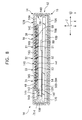
- Figs. 8 and 9 show another embodiment of the present invention, where the embodiment herein differs from that illustrated in Fig. 2 in that an edge portion 141R of the upper sheet 141 is electrically connected to an upper end plane of the electrical connection portion 190 through a hole 14F provided to the portion 14B of the upper enclosure portion 14.That is, each of the electrical wiring portions 200 to 204 of the upper sheet, 141 is connected to each of the electrical wiring portions 300 to 304 on the circuit board 170 via each of the conductive members 260 to 264, while the electrical wiring portions 200 to 204 at the edge portion 141R of the upper sheet 141 as shown in Fig. 6 being clamped between the upper end plane of the electrical connection portion 190 and the portion 14B.
- the embodiment illustrated in Figs. 8 and 9 differs from that in Fig. 2 only in the above point and residual points are the same, so that the same explanation with same symbols will apply to the residual parts.
- Fig. 10 shows an example of the sheet-type switch portion 140 positioned to the portion 14A or 14B of the upper enclosure portion 14 shown in Fig. 2 or Fig. 8. That is, the portion 14A or 14B has a plurality of pins 350, and the sheet-type switch portion 140 is positioned through engagement with these pins 350.
- Fig. 11 shows an example of the sheet-type switch portion 140 positioned through engagement with a projection 130T formed on the inner section 130 of the upper enclosure portion 14.
- Fig. 12 shows an example of the sheet-type switch portion 140 having on the lower sheet 142 thereof, instead of on the upper surface of the upper sheet 141 thereof, the electrical wiring portions 200 to 204 as shown in Fig. 6.
- the lower sheet 142 is electrically connected to the upper end plane of the electrical connection portion 190 through a hole 380 provided to the receiving portion 14E. Since the electrical wiring portions 200 to 204 are formed on the upper surface of the lower sheet 142, the lower sheet 142 is electrically connected to an upper end of the electrical connection portion 190 as folded once at 180° . That is, the electrical wiring portions 200 to 204 are electrically connected individually to one ends of the conductive members 260 to 264 through the folded portion 142A of the lower sheet 142.
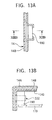
- Figs. 13A and 13B show an example of the electrical connection portion 190 fixed, for example, to the portion 14B of the upper enclosure portion 14 shown Fig. 2
- the position of the electrical connection portion 190 can be positioned with respect to the upper enclosure portion 14.
- the electrical connection between the sheet-type switch portion 140 and the circuit board 170 is achieved by engaging the lower enclosure portion 16 holding the circuit board 170 and the upper enclosure portion 14.
- the electrical connection portion 190 now can be independent of the upper enclosure portion 14 if the electrical connection portion 190 made of a conductive rubber is press fit in some degree to the attachment portion 222 for positioning the upper enclosure portion 14.
- Fig. 14 shows an exemplary electrical connection between the input device 18 and the individual components of the electronic apparatus 10 previously shown in Fig. 1.
- a microcomputer 80 dedicated for key input
- a general control microcomputer 84 for controlling the operation of the input device 18 and the individual components of the electronic apparatus 10 previously shown in Fig. 1.
- a memory 86 for storing, for example, arbitrary music information
- a music information amplifying output portion 88 for storing, for example, arbitrary music information.
- the microcomputers 80 and 84, the memory 86 and the music information amplifying output portion 88 compose a circuit unit 90, and the circuit unit 90 is located in an inner space of the enclosure 12.
- the microcomputer 80 is connected to the switch contact points 50 to 54 of the sheet-type switch portion 140 previously shown in Fig. 2.
- the microcomputer 80 is also connected to the general control microcomputer 84.
- the memory 86 is connected to the general control microcomputer 84.
- the microcomputer 84 controls the microcomputer 80, memory 86 and music information amplifying output portion 88.
- the microcomputer 84 is connected to the music information amplifying output portion 88.
- the music information amplifying output portion 88 amplifies music information received from the memory 86 via the microcomputer 84 and then outputs the information to the output portion 92 such as a headphone or earphone. The user is able to listen to the music information through the output portion 92.
- the information output from the output portion 92 may of course not only the music information but also other type of audible information.
- a semiconductor memory for example, and any other type of memory are applicable as the memory 86.
- the memory 86 may be fixed to the circuit unit 90, or may be composed so as to be detachable from the circuit unit 90. It is also possible to directly store music or other information in the memory 86 through a communication network such as internet.
- DRAM dynamic random access memory
- SRAM static random access memory
- Hard disk is the typical of other type of memory.
- Fig. 15 shows an exemplary connection between the microcomputer 80 and switch contact points 50 to 54 previously shown in Fig. 14.
- the switch contact points 50 to 54 are denoted as key0 to key4.
- the switch contact points 50 to 54 are individually connected to ports P10 to P14 of the microcomputer 80 as shown in Fig. 15. Port P20 of the microcomputer is connected to a common electrode 68 for the switch contact points 50 to 54.
- Input key code VOL+ in Table (A) in Fig. 15 enables raising of the sound level from the music information amplifying output portion 88, the corresponding output voltage ratio being 0.5.
- Input key code VOL- enables lowering of the sound level, the corresponding output voltage ratio being 0.57.
- Input key code STOP stops playback of music information, the corresponding output voltage ratio being 0.59.
- Input key code PLAY/FF enables transfer of music information from the memory 86, shown in Fig. 14, to the output portion 92 and fast -forward of the music information, the corresponding output voltage ratio being 0.73.
- Input key code REW enables recovering the rewind position of music information from the memory 86, shown in Fig. 14, the corresponding output voltage ratio being 0.91.
- output voltage ratio output voltage ratio X Vcc where, Vcc is a reference voltage and is typically 5 V.
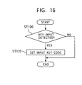
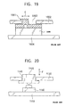
- Fig. 16 shows an exemplary key input operation f or the input device 18 previously shown in Figs. 1 to 3.
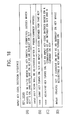
- Fig. 17 shows an exemplary input key code decision table.
- step ST100 a key input is detected in step ST100 in Fig. 16, which-is actually done by the switch contact points 50 to 54 in Fig. 2, an input key code listed in Fig. 17 is set in step ST120.
- the exemplary input key code decision table of Fig. 17 shows key initially turned ON in column (A), current ON key in column (B) and applied input key code in column (C).
- the input key code decision table of Fig. 17 also has columns (D), (E) and (F).
- Column (D) shows various key codes defined by combinations of the key initially turned ON in column (A) and the current ON key in column (B). For example, when the key initially turned ON is key0 and current ON key defined within a predetermined period is again key0, that is, when the same key was pressed twice within a predetermined period, the input key code will be VOL+ (raising sound level).
- Key2 for the key initially turned ON and key2 for the current ON key defined within a predetermined period will result in an input key code of STOP (cessation of playback of music information); and key 4 for the key initially turned ON and key4 for the current ON key defined within a predetermined period will result in an input key code of VOL-(lowering sound level).
- Column (E) of Fig. 17 indicates that combination of different keys for the key initially turned ON and the current ON key defined within a predetermined period will yield an input key code PLAY/FF. For example, when the key initially turned ON is key0 and the current ON key defined within a predetermined period is key0, the input key code will be PLAY (playback operation of music information) /FF (fast -forward to playback position of music information).
- While Column (E) corresponds to the cases in which the key initially turned ON is smaller than the current ON key, Column (F) on the contrary corresponds to the cases in which the key initially turned ON is larger than the current ON key.
- the input key code will be REW (rewind namely back to position of music information). For example, when the key initially turned ON is key4 and the current ON key defined within a predetermined period is key3, the input key code will be REW.
- Fig. 18 shows an exemplary input key code decision sequence.
- the microcomputer 80 previously shown in Fig. 15 scans the ports P 10 to P 14 to detect ON state thereof, and sets those in the ON state as the initially ON keys.
- chattering elimination, noise isolation and other software-base processing internally proceed at that time so as to avoid false recognition of pressing the key despite no human intention of pressing the key, or to avoid false judgment of pressing the key interfered by external electromagnetic noise.
- the switch will be pressed again according to the modes shown in columns (B) to (D), that is, any key will be pressed within a predetermined period.
- FIG. D of Fig. 18 indicates other key operation, in which a. current ON key is set as an initially ON key while neglecting the function of a key initially turned ON.
- a. current ON key is set as an initially ON key while neglecting the function of a key initially turned ON.
- One typical case relates to that the current ON key shown in column (A) of Fig. 17 is pressed after an elapse of a predetermined period after pressing the key initially turned ON.
- the user serially presses the key tops 30 to 34 with the finger by scanning along the longitudinal direction X1 of the slit portion 40 or the counter direction X2; or presses only one key top.
- the slit portion 40 shown in Figs. 2 and 3 can correctly guide the belly of the finger towards the key tops 30 to 34, which allows the user's finger surely touch the key tops 30 to 34. Since the slit portion 40 can support a part of the belly of the finger, the belly of the finger will never exert an unnecessary force on the sheet-type switch portion 140, which will successfully prevent properties of the sheet-type switch 140 and the switch contact points 50 to 54 from being degraded.
- the microcomputer 80 shown in Fig. 15 will send a control signal representing the input key code VOL+ to another microcomputer 84 shown in Fig. 14 according to the description in column (D) of Fig. 17.
- the microcomputer 84 will send a control signal to the music information amplifying output portion 88, which will raise the sound level of the music information output from the output portion 92.
- the input key code of PLAY/FF will come into effect as shown in column (E) of Fig. 17, and a control signal f or PLAY/FF will be sent from the microcomputer 80 to the microcomputer 84 shown in Fig. 14.
- a control signal f or PLAY/FF will be sent from the microcomputer 80 to the microcomputer 84 shown in Fig. 14.
- the music information stored in the memory 86 will be in playback from the output portion 92 with the aid of the microcomputer 84, or playback position thereof will be fed forward.
- the fast forward operation allows search for the beginning of the next title.
- the input key code of REW will come into effect by the microcomputer 80 as shown in column (F) of Fig. 17, and a control signal for REW will be sent from the microcomputer 80 to the microcomputer 84 shown in Fig. 14.
- the microcomputer 84 will recover a certain playback position of the music information stored in the memory 86.
- microcomputers 80 and 84 shown in Fig. 14 can be integrated into a single microcomputer.
- the input device 18 shown in Fig. 1 is provided for an electronic apparatus, and more specifically for a portable music playback device.
- a music playback device including such input device may be of hand-held type, arm-held type, pendant type or of other types.
- the input device of the present invention can be applicable not only to such electronic apparatus for playback music or music information, but also to a recording and playback apparatus for music information.
- the input device of the present invention still can be applicable not only to recording and playback of music information, but also to recording and playback apparatus of image and voice information, or to playback apparatus of image and voice information.
- the input device of the present invention still further can be applicable to electronic apparatus of other types or in other fields besides the applications described above.
Landscapes
- Push-Button Switches (AREA)
- Mounting Of Printed Circuit Boards And The Like (AREA)
- Input From Keyboards Or The Like (AREA)
Abstract
Description
Column (E) of Fig. 17 indicates that combination of different keys for the key initially turned ON and the current ON key defined within a predetermined period will yield an input key code PLAY/FF. For example, when the key initially turned ON is key0 and the current ON key defined within a predetermined period is key0, the input key code will be PLAY (playback operation of music information) /FF (fast -forward to playback position of music information).
Claims (10)
- An input device (18) for entering a desired command comprising:an enclosure (12) having a slit portion (40);a sheet-type switch portion (140) located within said enclosure so as to be aligned with said slit portion;a circuit board (170) located within said enclosure; andelectrical connection portion (190) which establishes electrical connection between said circuit board and said sheet-type switch portion by elastic deformation caused by assembly process of said enclosure.
- The input device as claimed in Claim 1, wherein said enclosure comprises an outer section (120) and an inner section (130) located inside the outer section, and said sheet-type switch portion is fixed between the outer section and the inner section.
- The input device as claimed in Claim 2, wherein said electrical connection portion comprisesan elastic insulating member (280); anda plurality of conductive members (260-264) provided in said elastic insulating member, wherein said plurality of conductive members establish electrical connection between said sheet-type switch and said circuit board upon elastic deformation of said elastic insulating member.
- The input device as claimed in Claim 3, wherein said sheet-type switch has an electrical wiring portion (200) connected to one end of said conductive members of the electrical connection portion.
- The input device as claimed in Claim 3, wherein said circuit board has an electrical wiring portion (300) connected to the other end of said conductive members of the electrical connection portion.
- The input device as claimed in Claim 1, wherein said electrical connection portion (190) is connected to said sheet-type switch portion (140) through a hole (14D) provided to said inner section of the enclosure.
- The input device as claimed in Claim 1, wherein said sheet-type switch has an electrical wiring portion (200), said electrical wiring portion being connected to said electrical connection portion through a hole (14F) provided to said inner section of the enclosure.
- A method for fabricating an input device (18) for entering a desired command comprising the steps of:placing a sheet-type switch portion (140) in an enclosure (12) so as to correspond with a slit portion (40) provided to said enclosure; andestablishing electrical connection (190) between said sheet-type switch portion and a circuit board (170) housed in said enclosure through an electrical connection portion (200) by elastic deformation of said electrical connection portion caused by assembly process of said enclosure.
- A method for fabricating an input device as claimed in Claim 8, wherein said enclosure is composed of an outer section (120) and an inner section (130) located inside said outer section, and said sheet-type switch portion is fixed between said outer section and said inner section.
- A method for fabricating an input device as claimed in Claim 8, wherein said electrical connection portion (190) is composed of an elastic insulating member (280) and conductive members (260-264), and electrical connection is established between said sheet-type switch portion and said circuit board through said conductive members upon elastic deformation of said insulating member.
Applications Claiming Priority (2)
| Application Number | Priority Date | Filing Date | Title |
|---|---|---|---|
| JP24917399A JP2001077561A (en) | 1999-09-02 | 1999-09-02 | Input device and method of manufacturing input device |
| JP24917399 | 1999-09-02 |
Publications (2)
| Publication Number | Publication Date |
|---|---|
| EP1081729A2 true EP1081729A2 (en) | 2001-03-07 |
| EP1081729A3 EP1081729A3 (en) | 2002-12-11 |
Family
ID=17189003
Family Applications (1)
| Application Number | Title | Priority Date | Filing Date |
|---|---|---|---|
| EP00402399A Withdrawn EP1081729A3 (en) | 1999-09-02 | 2000-08-30 | Input device employing sheet type switch and method for fabricating thereof |
Country Status (4)
| Country | Link |
|---|---|
| EP (1) | EP1081729A3 (en) |
| JP (1) | JP2001077561A (en) |
| KR (1) | KR20010030204A (en) |
| CN (1) | CN1288350A (en) |
Cited By (4)
| Publication number | Priority date | Publication date | Assignee | Title |
|---|---|---|---|---|
| EP2081418A3 (en) * | 2008-01-17 | 2010-03-10 | Harris Corporation | Method for making three-dimensional liquid crystal polymer multilayer circuit boards |
| EP2081204A3 (en) * | 2008-01-17 | 2010-03-10 | Harris Corporation | Three-dimensional liquid crystal polymer multilayer circuit board including membrane switch and related methods |
| EP2081245B1 (en) * | 2008-01-17 | 2010-09-22 | Harris Corporation | Three-dimensional liquid crystal polymer multilayer circuit board including membrane switch and related manufacturing method |
| US10427256B2 (en) | 2011-03-31 | 2019-10-01 | Seiko Instruments Inc. | Printed substrate holding device |
Families Citing this family (1)
| Publication number | Priority date | Publication date | Assignee | Title |
|---|---|---|---|---|
| JP4517823B2 (en) * | 2004-11-11 | 2010-08-04 | アイシン精機株式会社 | Electronic components |
Family Cites Families (3)
| Publication number | Priority date | Publication date | Assignee | Title |
|---|---|---|---|---|
| US4368369A (en) * | 1980-03-14 | 1983-01-11 | Citizen Watch Co., Ltd. | Electrical switch |
| US5187647A (en) * | 1991-03-11 | 1993-02-16 | John Fluke Mfg. Co., Inc. | Electronic instrument keypad assembly with z-axis oriented electrical interconnect |
| GB2327908A (en) * | 1997-08-02 | 1999-02-10 | Motorola Gmbh | Keypad membrane having integrated elastomeric connectors |
-
1999
- 1999-09-02 JP JP24917399A patent/JP2001077561A/en not_active Withdrawn
-
2000
- 2000-08-30 EP EP00402399A patent/EP1081729A3/en not_active Withdrawn
- 2000-08-31 KR KR1020000051108A patent/KR20010030204A/en not_active Withdrawn
- 2000-09-02 CN CN00131729A patent/CN1288350A/en active Pending
Cited By (11)
| Publication number | Priority date | Publication date | Assignee | Title |
|---|---|---|---|---|
| EP2081418A3 (en) * | 2008-01-17 | 2010-03-10 | Harris Corporation | Method for making three-dimensional liquid crystal polymer multilayer circuit boards |
| EP2081204A3 (en) * | 2008-01-17 | 2010-03-10 | Harris Corporation | Three-dimensional liquid crystal polymer multilayer circuit board including membrane switch and related methods |
| EP2081245B1 (en) * | 2008-01-17 | 2010-09-22 | Harris Corporation | Three-dimensional liquid crystal polymer multilayer circuit board including membrane switch and related manufacturing method |
| EP2428971A1 (en) * | 2008-01-17 | 2012-03-14 | Harris Corporation | Three-dimensional liquid crystal polymer multilayer circuit board including membrane switch and related methods |
| US8778124B2 (en) | 2008-01-17 | 2014-07-15 | Harris Corporation | Method for making three-dimensional liquid crystal polymer multilayer circuit boards |
| US9117602B2 (en) | 2008-01-17 | 2015-08-25 | Harris Corporation | Three-dimensional liquid crystal polymer multilayer circuit board including membrane switch and related methods |
| US9922783B2 (en) | 2008-01-17 | 2018-03-20 | Harris Corporation | Method for making a three-dimensional liquid crystal polymer multilayer circuit board including membrane switch |
| US10818448B2 (en) | 2008-01-17 | 2020-10-27 | Harris Corporation | Method for making a three-dimensional liquid crystal polymer multilayer circuit board including membrane switch including air |
| US11657989B2 (en) | 2008-01-17 | 2023-05-23 | Harris Corporation | Method for making a three-dimensional liquid crystal polymer multilayer circuit board including membrane switch including air |
| US12400810B2 (en) | 2008-01-17 | 2025-08-26 | Harris Corporation | Method for making a three-dimensional liquid crystal polymer electronic device |
| US10427256B2 (en) | 2011-03-31 | 2019-10-01 | Seiko Instruments Inc. | Printed substrate holding device |
Also Published As
| Publication number | Publication date |
|---|---|
| EP1081729A3 (en) | 2002-12-11 |
| KR20010030204A (en) | 2001-04-16 |
| CN1288350A (en) | 2001-03-21 |
| JP2001077561A (en) | 2001-03-23 |
Similar Documents
| Publication | Publication Date | Title |
|---|---|---|
| US6307465B1 (en) | Input device | |
| RU2734386C2 (en) | Electronic device connecting unit | |
| EP1156643B1 (en) | Step keys, step key assembly, and terminal having the step key assembly | |
| US5214514A (en) | Compact video/sound apparatus with foldable screen | |
| US6794798B2 (en) | Display device and electronic equipment employing piezoelectric speaker | |
| WO2003088428A1 (en) | Jack | |
| US8634885B2 (en) | Mobile device having a plate in a gap between sliding bodies | |
| EP1081729A2 (en) | Input device employing sheet type switch and method for fabricating thereof | |
| JP2009514129A (en) | Socket assembly | |
| JP2002359890A (en) | Display device and electronic equipment | |
| US6542092B1 (en) | Keyboard with multiple input/output function | |
| CN112166401A (en) | Input device and electronic device including the same | |
| US6735377B1 (en) | Control device for CD player | |
| JP2001119777A (en) | Electronics | |
| JP4411707B2 (en) | Electronics | |
| JP2003031079A (en) | Input device and electronic apparatus having input device | |
| JP2000011812A (en) | Operation button device | |
| JP4315574B2 (en) | INPUT DEVICE AND ELECTRONIC DEVICE HAVING INPUT DEVICE | |
| KR200324866Y1 (en) | Apparatus for reproducing audio data | |
| JP2001307591A (en) | Key button structure for electronic equipment | |
| JP4115172B2 (en) | Switch mechanism | |
| WO1995028711A1 (en) | Multidirectional switch assembly for hand held recording devices | |
| JP2001117572A (en) | Electronics | |
| JP2002078061A (en) | Card type electronic equipment | |
| KR200241708Y1 (en) | Pen type Digital voice recoder |
Legal Events
| Date | Code | Title | Description |
|---|---|---|---|
| PUAI | Public reference made under article 153(3) epc to a published international application that has entered the european phase |
Free format text: ORIGINAL CODE: 0009012 |
|
| AK | Designated contracting states |
Kind code of ref document: A2 Designated state(s): AT BE CH CY DE DK ES FI FR GB GR IE IT LI LU MC NL PT SE |
|
| AX | Request for extension of the european patent |
Free format text: AL;LT;LV;MK;RO;SI |
|
| PUAL | Search report despatched |
Free format text: ORIGINAL CODE: 0009013 |
|
| AK | Designated contracting states |
Kind code of ref document: A3 Designated state(s): AT BE CH CY DE DK ES FI FR GB GR IE IT LI LU MC NL PT SE |
|
| AX | Request for extension of the european patent |
Free format text: AL;LT;LV;MK;RO;SI |
|
| STAA | Information on the status of an ep patent application or granted ep patent |
Free format text: STATUS: THE APPLICATION IS DEEMED TO BE WITHDRAWN |
|
| AKX | Designation fees paid | ||
| REG | Reference to a national code |
Ref country code: DE Ref legal event code: 8566 |
|
| 18D | Application deemed to be withdrawn |
Effective date: 20030301 |