EP1081675A2 - A power circuit for a liquid crystal display - Google Patents
A power circuit for a liquid crystal display Download PDFInfo
- Publication number
- EP1081675A2 EP1081675A2 EP00118146A EP00118146A EP1081675A2 EP 1081675 A2 EP1081675 A2 EP 1081675A2 EP 00118146 A EP00118146 A EP 00118146A EP 00118146 A EP00118146 A EP 00118146A EP 1081675 A2 EP1081675 A2 EP 1081675A2
- Authority
- EP
- European Patent Office
- Prior art keywords
- voltage
- output
- power circuit
- output voltage
- mosfet
- Prior art date
- Legal status (The legal status is an assumption and is not a legal conclusion. Google has not performed a legal analysis and makes no representation as to the accuracy of the status listed.)
- Granted
Links
Images



Classifications
-
- G—PHYSICS
- G09—EDUCATION; CRYPTOGRAPHY; DISPLAY; ADVERTISING; SEALS
- G09G—ARRANGEMENTS OR CIRCUITS FOR CONTROL OF INDICATING DEVICES USING STATIC MEANS TO PRESENT VARIABLE INFORMATION
- G09G3/00—Control arrangements or circuits, of interest only in connection with visual indicators other than cathode-ray tubes
- G09G3/20—Control arrangements or circuits, of interest only in connection with visual indicators other than cathode-ray tubes for presentation of an assembly of a number of characters, e.g. a page, by composing the assembly by combination of individual elements arranged in a matrix no fixed position being assigned to or needed to be assigned to the individual characters or partial characters
- G09G3/34—Control arrangements or circuits, of interest only in connection with visual indicators other than cathode-ray tubes for presentation of an assembly of a number of characters, e.g. a page, by composing the assembly by combination of individual elements arranged in a matrix no fixed position being assigned to or needed to be assigned to the individual characters or partial characters by control of light from an independent source
- G09G3/36—Control arrangements or circuits, of interest only in connection with visual indicators other than cathode-ray tubes for presentation of an assembly of a number of characters, e.g. a page, by composing the assembly by combination of individual elements arranged in a matrix no fixed position being assigned to or needed to be assigned to the individual characters or partial characters by control of light from an independent source using liquid crystals
- G09G3/3611—Control of matrices with row and column drivers
- G09G3/3696—Generation of voltages supplied to electrode drivers
Definitions
- the invention relates to a power circuit for performing impedance conversion of a given voltage to provide an output, in particular to a power circuit for use in a liquid crystal display (LCD) apparatus which requires a multiplicity of voltage sources.
- LCD liquid crystal display
- Apparatuses have been commonly used as display means for portable communication devices such as cellular phones and pagers.
- a drive circuit is used to drive a multiplicity of display elements or pixels in a given duty cycle using a multiplicity of bias voltages as shown in Fig. 1.
- the LCD apparatus of Fig. 1 comprises:
- An LCD apparatus having such arrangement must be operated at a low power on one hand in order to maximize the life of the LCD as much as possible, but on the other hand, in order to provide a good display quality, it must be operable by a large driving power to prevent deterioration of output waveforms especially for a large capacitate load.
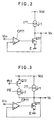
- a constant current source I11 connected between the source voltage Vdd and the ground voltage E are a constant current source I11 and an N channel MOSFET Q11 connected in series with each other, providing at the node therebetween an output voltage Vo.
- a difference amplifier CP11 is also provided in the power circuit, having a negative or inverting input terminal for receiving an input voltage Vin and a positive or non-inverting input terminal for receiving the output voltage Vo, and generating a gate voltage for the MOSFET Q11.
- a constant current i1 is provided from the constant current source I11.
- the input voltage Vin and the output voltage Vo are compared in the difference amplifier CP11 to control switching operation of the MOSFET Q11.
- the output voltage Vo is controlled to balance the input voltage Vin.
- the MOSFET Q11 is turned on by the output voltage of the difference amplifier CP11 to lower the output voltage Vo, until the output voltage Vo balances the input voltage Vin.
- the ability of the circuit to lower the output voltage Vo raised by a positive noise depends on the driving power of the MOSFET Q11.
- the MOSFET Q11 is turned off by the output of the difference amplifier CP11, and as a result, a constant current i1 is supplied from the constant current source I11, which gradually pushes up the output voltage Vo.
- the output level of the difference amplifier CP11 will become high to turn the MOSFET Q11 as the output voltage Vo equals the input voltage Vin, thereby keeping the output voltage Vo at the same level of the input level Vin.
- the ability of the power circuit to raise lowered output voltage Vo is determined by the magnitude of the constant current i1 from the constant current source I11.
- MOSFET Q11 keeps the current i1 flowing to have the output voltage Vo balancing the input voltage Vin.
- Fig. 3 illustrates a conventional circuit with an improvement to overcome such problem as discussed above in conjunction with Fig. 2, in which a P channel MOSFET Q12 and a further constant current source I12 are connected in parallel with the constant current source I11.
- the basic structure and function of the improved circuit are the same as those of Fig. 2.
- the MOSFET Q12 is supplied at the gate thereof with a periodic control signal for turning on the MOSFET Q12 at times when noises are supposedily likely to superpose on the output voltage Vo, thereby turning on the MOSFET Q12 to provide an extra constant current i2 from the constant current source I12 superposing on the constant current i1 from the constant current source I11, which adds to the power circuit a counteractive power against L-noises.
- the MOSFET Q12 is turned on periodically, irrespective of whether a noise exists affecting the output voltage Vo or not. Hence, although anti-L noise capacity is improved a little, the improvement cannot be a fundamental solution to the drive circuit for LCD apparatus.
- a power circuit comprising:
- the second switching element Q42 of the power circuit is turned on in raising the output voltage Vo, so that the power needed to run a load is significantly reduced as compared with conventional constant current type power circuits.
- the hysteresis of the second comparator CP42 controlling the second switching element Q42 may improve noise reduction, and hence output distortions caused by the noise in the power circuit.
- the power circuit may be provided, between the input end of the second comparator CP42 for receiving the reference voltage and either one of the voltage supplies, with a resistor and a third switching element which is controlled by the output of the second comparator CP42.
- the reference voltage to the second comparator CP42 is automatically switched between two levels in accordance with the output of the second comparator CP42.
- the arrangement adds to the second comparator CP42 a hysteresis character with respect to the output voltage Vo.
- the third switching element Q43 as well as the first and the second switching elements Q41 and Q42, respectively, can be MOSFETs.
- first switching element Q41 can be an N channel MOSFET while the second switching element Q42 can be a P channel MOSFET.
- the power circuit having this arrangement can control the switching elements involved at a very low power in response to the output voltages of the first and the second comparators CP41 and CP42, respectively.
- FIG. 4 there is shown an exemplary power circuit according to the invention for use as voltage followers for example.
- a P channel MOSFET Q42 and an N channel MOSFET Q41 are connected in series between a first voltage supply providing a supply voltage Vdd and a second voltage supply E providing the ground voltage, to generate at the node A thereof an output voltage Vo.
- the MOSFET Q42 serves as a switch for supplying electric power to a capacitive load such as a common electrode of an LCD selectively connected to the node A, while the MOSFET Q41 serves as a switch for draining electric energy from the load.
- the difference amplifier CP41 serves as a comparator comparing the two inputs to generate an output, which is supplied to the gate of the MOSFET Q41.
- the inverting input terminal of the difference amplifier CP42 is supplied with a reference voltage Vref which selectively assumes either a high reference voltage Vref1 or a low reference voltage Vref2 in accordance with the condition of the power circuit.
- the output voltage Vo is input to the non-inverted input terminal of the difference amplifier CP42 serving as a comparator.
- the output voltage Vo is compared with the reference voltage.
- the output of the comparator (potential at point C) is applied to the gate of the MOSFET Q42.
- resistors R41 and R42 Connected between the voltage supply at voltage Vdd and the ground at voltage E are resistors R41 and R42 connected in series.
- a resistor R43 and an N channel MOSFET Q43 connected in series with each other is connected in parallel with the resistor R42.
- point B has a reference voltage which equals either Vdd ⁇ R42/(R41 + R42) (referred to as the high reference voltage Vref1) or Vdd ⁇ (R42 ⁇ R43)/(R41 ⁇ R42 + R42 ⁇ R43 + R43 ⁇ R41) (referred to as lower reference voltage Vref2), depending on whether the MOSFET Q43 is turned on or off.
- Vref1 Vdd ⁇ R42/(R41 + R42)
- Vref2 lower reference voltage
- the gate of the MOSFET Q43 is connected to the output of the difference amplifier CP42, so that the gate has the same voltage as the output. Hence the difference amplifier CP42 exhibits a hysteresis.
- the high reference voltage Vref1 is the same as the input voltage Vin. Any one of the outputs of the bias circuit 11 of LCD apparatus shown in Fig. 1 can be used as the input voltage Vin.
- This power circuit may be used as a drive circuit of an LCD apparatus in driving capacitive loads, where various bias voltages are generated and used in combination.
- the power circuit shown in Fig. 4 may provide such bias voltage, thus, under the influences of these bias voltages, the output voltage Vo deviates from a predetermined level because it is pushed up by H noises or pull down by L noises.
- the output voltage Vo is substantially the same as the input voltage Vin, and the MOSFET Q42 is turned off.
- the condition of the MOSFET Q41 is indefinite in that it can assume ON state and OFF state equally well. Meanwhile, the output of the difference amplifier CP42 is at H level and the MOSFET Q43 is in ON state, so that the B point voltage equals the lower reference voltage Vref2.
- the output voltage Vo tends to decrease.
- the output voltage Vo is lowered to the level of the reference voltage Vref2
- the output of the difference amplifier CP42 is inverted, generating at the output terminal thereof a low level voltage L. Consequently, the MOSFET Q42 is turned ON, resulting in a current flowing from the voltage supply at Vdd through the MOSFET Q42.
- the MOSFET Q43 is turned OFF, providing the difference amplifier CP42 with the high reference voltage Vref1.
- the MOSFET Q41 is turned OFF since then the output voltage of the MOSFET Q41 is low L.
- the output of the difference amplifier CP42 is inverted to high level H. This turns the MOSFET Q42 off and the MOSFET Q43 on, so that the reference voltage Vref for the difference amplifier CP42 becomes low Vref2, thereby allowing the power circuit to restore the normal operating condition.
- the difference amplifier CP42 has a hysteresis with respect to the output voltage Vo.
- the MOSFET Q41 As the MOSFET Q41 is turned on, a current is drawn from the load. Meanwhile, the output voltage Vo increases above the input voltage Vin due to the energy of the H noise, and begins to decrease later at time t5. The output voltage Vo will further decrease, until it balances the input voltage Vin at t6 say to turn off the MOSFET Q41, allowing the power circuit to return to the normal operating condition.
- the power circuit of the invention advantageously operates as describe above, owing to the hysteresis character of the difference amplifier CP42.
- This feature of the invention will be better understood by comparing the invention with a referential circuit as shown in Figs. 6, having no hysteresis character.
- the behavior of the circuit of Fig. 6 is shown in Fig. 7.
- the referential circuit shown in Fig. 6 has the same structure as the inventive circuit shown in Figs. 4 and 5 except that the former circuit has only one reference voltage Vref.
- the reference voltage Vref is set a little lower than that of the input voltage Vin. Since the driving power of the MOSFET Q42 is made as large as that of the MOSFET Q41 to enable quick absorption of noise from the load, this lower setting of the reference voltage is necessary because otherwise the MOSFET Q41 and the MOSFET Q42 would be simultaneously conducted, resulting in a large current between the voltage supply at Vdd and the ground.
- the output voltage Vo is further lowered below the reference voltage Vref, until the energy is exhausted at time t2 when the output voltage Vo begins to rise.
- the output voltage Vo overshoots the input voltage Vin due to the energy of the H noise at t5, and thereafter begins to decrease as shown in Fig. 7.
- the output voltage Vo continues to decrease until it balances the input voltage Vin at time t6, when the MOSFET Q41 is turned off to restore the normal operating condition of the power circuit.
- the power circuit can recover the output voltage only up to the reference voltage Vref if the difference amplifier CP42 has no hysteresis character. Therefore, the distortion in the output of the power circuit caused by an L noise remains as much as (Vin - Vref), unless an H noise follows the L noise as shown in Fig. 7. However, one may not always anticipate such H noise to restore the output.
- the reference voltage Vref could be set equal to or close to the input voltage Vin.
- the invention allows the MOSFET Q42 to be turned on only when a current is required for the load or for raising the lowered output voltage Vo to the normal level, as described in conjunction with Figs. 4 and 5. This implies that the impedance of the MOSFET Q42 can be very small.
- the power circuit of the invention can provide a much greater current to the load as compared with conventional constant current type power circuits, which implies that the power circuit of the invention has an enhanced driving power to a highly capacitive load.
- the power circuit of the invention can minimize the influences of both H noises and L noises. It should be appreciated that the output voltage Vo can be set to a given input voltage Vin from above and below Vin, corrected to the level of the input voltage Vin if the output voltage is deviated above or below Vin.
- the current providing MOSFET Q42 and the current absorbing MOSFET Q41 are conditioned not to be conductive simultaneously by the respective difference amplifiers CP41 and CP42, so that an inter-source current will never be incurred.
- the power consumption by the power circuit will be negligibly small if the load is capacitive.
- the invention enables a design of a compact power circuit which includes advantageously smaller elements such as MOSFETs consuming only a small amount of electric energy.
Landscapes
- Engineering & Computer Science (AREA)
- Chemical & Material Sciences (AREA)
- Crystallography & Structural Chemistry (AREA)
- Physics & Mathematics (AREA)
- Computer Hardware Design (AREA)
- General Physics & Mathematics (AREA)
- Theoretical Computer Science (AREA)
- Liquid Crystal Display Device Control (AREA)
- Control Of Indicators Other Than Cathode Ray Tubes (AREA)
- Continuous-Control Power Sources That Use Transistors (AREA)
- Amplifiers (AREA)
Abstract
Description
Claims (4)
- A power circuit comprising:a first switching element Q41 connected between an output terminal of said power circuit and a first voltage supply E;a second switching element Q42 connected between a second voltage supply having voltage Vdd and said output terminal;a first comparator CP41 for comparing an input voltage Vin with an output voltage Vo at said output terminal, to turn on said first switching element Q41 if said output voltage Vo exceeds said input voltage Vin;a second comparator CP42 for comparing said output voltage Vo with a reference voltage Vref, to turn on said second switching element Q42 if said output voltage Vo becomes lower than the reference voltage Vref, wherein said second comparator CP42 exhibits a hysteresis in the operation.
- The power circuit as set forth in claim 1, further comprising, between the input end of said second comparator CP42 for receiving said reference voltage and either one of said voltage supplies, with a resistor and a third switching element which is controlled by the output of said second comparator CP42.
- The power circuit as set forth in claim 2, wherein said first, second and third switching elements (Q41, Q42, and Q43) are MOSFETs.
- The power circuit as set forth in claim 3, wherein said first switching element (Q41) is an N channel MOSFET while said second switching element (Q42) is a P channel MOSFET.
Applications Claiming Priority (2)
| Application Number | Priority Date | Filing Date | Title |
|---|---|---|---|
| JP24250999A JP3781924B2 (en) | 1999-08-30 | 1999-08-30 | Power circuit |
| JP24250999 | 1999-08-30 |
Publications (3)
| Publication Number | Publication Date |
|---|---|
| EP1081675A2 true EP1081675A2 (en) | 2001-03-07 |
| EP1081675A3 EP1081675A3 (en) | 2002-01-02 |
| EP1081675B1 EP1081675B1 (en) | 2003-04-02 |
Family
ID=17090171
Family Applications (1)
| Application Number | Title | Priority Date | Filing Date |
|---|---|---|---|
| EP00118146A Expired - Lifetime EP1081675B1 (en) | 1999-08-30 | 2000-08-29 | Voltage follower for a liquid crystal display |
Country Status (4)
| Country | Link |
|---|---|
| US (1) | US6426670B1 (en) |
| EP (1) | EP1081675B1 (en) |
| JP (1) | JP3781924B2 (en) |
| DE (1) | DE60001885T2 (en) |
Cited By (1)
| Publication number | Priority date | Publication date | Assignee | Title |
|---|---|---|---|---|
| WO2018188175A1 (en) * | 2017-04-11 | 2018-10-18 | 惠科股份有限公司 | Overcurrent protection circuit, display panel, and display apparatus |
Families Citing this family (15)
| Publication number | Priority date | Publication date | Assignee | Title |
|---|---|---|---|---|
| JP3832627B2 (en) * | 2000-08-10 | 2006-10-11 | シャープ株式会社 | Signal line driving circuit, image display device, and portable device |
| JP3539940B2 (en) | 2001-07-30 | 2004-07-07 | 沖電気工業株式会社 | Voltage regulator |
| JP3800050B2 (en) * | 2001-08-09 | 2006-07-19 | 日本電気株式会社 | Display device drive circuit |
| US6690148B2 (en) * | 2001-11-28 | 2004-02-10 | Micron Technology, Inc. | Method and circuit for limiting a pumped voltage |
| JP2003168290A (en) * | 2001-11-29 | 2003-06-13 | Fujitsu Ltd | Power supply circuit and semiconductor device |
| US7102608B2 (en) * | 2002-06-21 | 2006-09-05 | Himax Technologies, Inc. | Method and related apparatus for driving pixels located in a row of an LCD panel toward the same average voltage value |
| JP3960848B2 (en) * | 2002-04-17 | 2007-08-15 | 株式会社ルネサステクノロジ | Potential generator |
| JP3910579B2 (en) * | 2003-12-08 | 2007-04-25 | ローム株式会社 | Display device driving device and display device using the same |
| JP4215254B2 (en) * | 2004-02-20 | 2009-01-28 | 沖電気工業株式会社 | Comparison circuit |
| ATE494577T1 (en) * | 2004-07-14 | 2011-01-15 | Nxp Bv | COMMON MODE VOLTAGE GENERATOR FOR A BATTERY POWERED HANDSET |
| JP5224702B2 (en) * | 2006-03-13 | 2013-07-03 | キヤノン株式会社 | Pixel circuit and image display device having the pixel circuit |
| JP2009211052A (en) * | 2008-02-06 | 2009-09-17 | Canon Inc | Drive circuit of display panel and display apparatus |
| JP4666010B2 (en) * | 2008-06-12 | 2011-04-06 | セイコーエプソン株式会社 | Load drive circuit and inkjet printer |
| US8080983B2 (en) * | 2008-11-03 | 2011-12-20 | Microchip Technology Incorporated | Low drop out (LDO) bypass voltage regulator |
| KR101226275B1 (en) * | 2011-02-28 | 2013-01-25 | 에스케이하이닉스 주식회사 | Internal voltage generation circuit |
Family Cites Families (7)
| Publication number | Priority date | Publication date | Assignee | Title |
|---|---|---|---|---|
| US5087834A (en) * | 1990-03-12 | 1992-02-11 | Texas Instruments Incorporated | Buffer circuit including comparison of voltage-shifted references |
| US5317254A (en) * | 1992-09-17 | 1994-05-31 | Micro Control Company | Bipolar power supply |
| JP3234043B2 (en) * | 1993-05-10 | 2001-12-04 | 株式会社東芝 | Power supply circuit for driving LCD |
| JPH0974347A (en) * | 1995-06-26 | 1997-03-18 | Mitsubishi Electric Corp | MOS integrated circuit |
| JP2806324B2 (en) * | 1995-08-25 | 1998-09-30 | 日本電気株式会社 | Internal step-down circuit |
| KR100186344B1 (en) * | 1996-10-18 | 1999-04-15 | 문정환 | Hysteresis Input Buffer |
| US5959475A (en) * | 1998-01-13 | 1999-09-28 | Xerox Corporation | Complementary push-pull CMOS source follower analog video buffer |
-
1999
- 1999-08-30 JP JP24250999A patent/JP3781924B2/en not_active Expired - Fee Related
-
2000
- 2000-08-29 EP EP00118146A patent/EP1081675B1/en not_active Expired - Lifetime
- 2000-08-29 DE DE60001885T patent/DE60001885T2/en not_active Expired - Lifetime
- 2000-08-29 US US09/650,295 patent/US6426670B1/en not_active Expired - Lifetime
Cited By (1)
| Publication number | Priority date | Publication date | Assignee | Title |
|---|---|---|---|---|
| WO2018188175A1 (en) * | 2017-04-11 | 2018-10-18 | 惠科股份有限公司 | Overcurrent protection circuit, display panel, and display apparatus |
Also Published As
| Publication number | Publication date |
|---|---|
| JP2001067133A (en) | 2001-03-16 |
| JP3781924B2 (en) | 2006-06-07 |
| EP1081675A3 (en) | 2002-01-02 |
| DE60001885T2 (en) | 2003-11-13 |
| DE60001885D1 (en) | 2003-05-08 |
| US6426670B1 (en) | 2002-07-30 |
| EP1081675B1 (en) | 2003-04-02 |
Similar Documents
| Publication | Publication Date | Title |
|---|---|---|
| EP1081675B1 (en) | Voltage follower for a liquid crystal display | |
| US6310616B1 (en) | Voltage generating circuit, and common electrode drive circuit signal line drive circuit and gray-scale voltage generating circuit for display device | |
| US20210200252A1 (en) | Adjuster and chip | |
| US6496175B1 (en) | Output circuit | |
| US6157360A (en) | System and method for driving columns of an active matrix display | |
| US7420356B2 (en) | Current direction detection circuit and switching regulator having the same | |
| JP4757623B2 (en) | Power circuit | |
| US20070040855A1 (en) | Display control apparatus capable of decreasing the size thereof | |
| US7701281B1 (en) | Flyback capacitor level shifter feedback regulation for negative pumps | |
| US20040095105A1 (en) | Power supply device and liquid crystal display device using the same | |
| WO1998040873A9 (en) | System and method for driving columns of an active matrix display | |
| US20060164374A1 (en) | Source driver and source driving method | |
| US7423479B2 (en) | Offset canceller for compensating for offset in signal output | |
| JPH0819250A (en) | Power supply apparatus | |
| KR100270033B1 (en) | Charging apparatus and current/voltage detector for use therein | |
| US6621439B1 (en) | Method for implementing a segmented current-mode digital/analog converter with matched segment time constants | |
| JP2003114727A (en) | Power supply circuit | |
| US6118261A (en) | Slew rate control circuit | |
| JPH1124764A (en) | DC stabilized power supply | |
| KR20000020856A (en) | Thin film transistor liquid crystal display having circuit for stabilizing driving power source | |
| JP7791049B2 (en) | Voltage amplifier circuit and circuit module | |
| US7609105B2 (en) | Voltage level generating device | |
| CN113359915B (en) | Low dropout linear voltage stabilizing circuit, chip and electronic equipment | |
| US20050046447A1 (en) | Hysteresis circuits used in comparator | |
| JP2000098331A (en) | Drive source device for liquid crystal display |
Legal Events
| Date | Code | Title | Description |
|---|---|---|---|
| PUAI | Public reference made under article 153(3) epc to a published international application that has entered the european phase |
Free format text: ORIGINAL CODE: 0009012 |
|
| AK | Designated contracting states |
Kind code of ref document: A2 Designated state(s): DE Kind code of ref document: A2 Designated state(s): AT BE CH CY DE DK ES FI FR GB GR IE IT LI LU MC NL PT SE |
|
| AX | Request for extension of the european patent |
Free format text: AL;LT;LV;MK;RO;SI |
|
| PUAL | Search report despatched |
Free format text: ORIGINAL CODE: 0009013 |
|
| AK | Designated contracting states |
Kind code of ref document: A3 Designated state(s): AT BE CH CY DE DK ES FI FR GB GR IE IT LI LU MC NL PT SE |
|
| AX | Request for extension of the european patent |
Free format text: AL;LT;LV;MK;RO;SI |
|
| 17P | Request for examination filed |
Effective date: 20020301 |
|
| GRAH | Despatch of communication of intention to grant a patent |
Free format text: ORIGINAL CODE: EPIDOS IGRA |
|
| AKX | Designation fees paid |
Free format text: DE |
|
| RTI1 | Title (correction) |
Free format text: VOLTAGE FOLLOWER FOR A LIQUID CRYSTAL DISPLAY |
|
| GRAH | Despatch of communication of intention to grant a patent |
Free format text: ORIGINAL CODE: EPIDOS IGRA |
|
| GRAA | (expected) grant |
Free format text: ORIGINAL CODE: 0009210 |
|
| AK | Designated contracting states |
Designated state(s): DE |
|
| REG | Reference to a national code |
Ref country code: IE Ref legal event code: FG4D |
|
| REF | Corresponds to: |
Ref document number: 60001885 Country of ref document: DE Date of ref document: 20030508 Kind code of ref document: P |
|
| PLBE | No opposition filed within time limit |
Free format text: ORIGINAL CODE: 0009261 |
|
| STAA | Information on the status of an ep patent application or granted ep patent |
Free format text: STATUS: NO OPPOSITION FILED WITHIN TIME LIMIT |
|
| 26N | No opposition filed |
Effective date: 20040105 |
|
| REG | Reference to a national code |
Ref country code: IE Ref legal event code: MM4A |
|
| PGFP | Annual fee paid to national office [announced via postgrant information from national office to epo] |
Ref country code: DE Payment date: 20090827 Year of fee payment: 10 |
|
| REG | Reference to a national code |
Ref country code: DE Ref legal event code: R119 Ref document number: 60001885 Country of ref document: DE Effective date: 20110301 |
|
| PG25 | Lapsed in a contracting state [announced via postgrant information from national office to epo] |
Ref country code: DE Free format text: LAPSE BECAUSE OF NON-PAYMENT OF DUE FEES Effective date: 20110301 |