EP1081498A1 - Scan latch circuit - Google Patents
Scan latch circuit Download PDFInfo
- Publication number
- EP1081498A1 EP1081498A1 EP00302835A EP00302835A EP1081498A1 EP 1081498 A1 EP1081498 A1 EP 1081498A1 EP 00302835 A EP00302835 A EP 00302835A EP 00302835 A EP00302835 A EP 00302835A EP 1081498 A1 EP1081498 A1 EP 1081498A1
- Authority
- EP
- European Patent Office
- Prior art keywords
- input
- scan
- latch
- scan latch
- circuitry
- Prior art date
- Legal status (The legal status is an assumption and is not a legal conclusion. Google has not performed a legal analysis and makes no representation as to the accuracy of the status listed.)
- Granted
Links
- 238000012360 testing method Methods 0.000 claims abstract description 32
- 230000015654 memory Effects 0.000 claims description 19
- 238000010586 diagram Methods 0.000 description 1
- 238000000034 method Methods 0.000 description 1
Images
Classifications
-
- G—PHYSICS
- G01—MEASURING; TESTING
- G01R—MEASURING ELECTRIC VARIABLES; MEASURING MAGNETIC VARIABLES
- G01R31/00—Arrangements for testing electric properties; Arrangements for locating electric faults; Arrangements for electrical testing characterised by what is being tested not provided for elsewhere
- G01R31/28—Testing of electronic circuits, e.g. by signal tracer
- G01R31/317—Testing of digital circuits
- G01R31/3181—Functional testing
- G01R31/3185—Reconfiguring for testing, e.g. LSSD, partitioning
- G01R31/318533—Reconfiguring for testing, e.g. LSSD, partitioning using scanning techniques, e.g. LSSD, Boundary Scan, JTAG
- G01R31/318541—Scan latches or cell details
Definitions
- the present invention relates to a scan latch circuit useable where alternative testing methods are employed on an associated circuit, and to the combination of such a scan latch circuit with an associated circuit.
- Scan latches are known components of test circuitry for circuits, and especially complex circuits such as memories.
- Such scan lathes typically have a two-input multiplexer with a control input for selecting between those two inputs from the output of the multiplexer feeding to latch circuitry.
- the control input receives a two state signal called scan enable, so that when it is a logical 1 state the second input, the scan input is applied from the multiplexer output to the latch circuitry.
- scan enable input is at logical 0, the first input, the data input is provided by the multiplexer to the latch circuitry.
- scan latches are used with a built-in self-test (BIST) arrangement - so that both scan test and built-in self-test (BIST) can be used - it is conventional to connect an input multiplexer to the first input of the scan latch, the input multiplexer having a first input for data output from the memory, a second input for the built-in self-test data from the memory and a control input for selecting between the two inputs.
- BIST built-in self-test
- Such a scan latch circuit is disadvantageous in that an additional gate delay is built in to the memory data path.
- a scan latch circuit for a circuit having a data output and first and second outputs for test information
- the scan latch circuit comprising a scan latch having first and second inputs and a control input for selecting between said first and second inputs for input to latch circuitry of said scan latch, the circuit further having first and second select signal inputs for selecting first and second test modes in which a respective one of said first and second test information is passed to said latch circuitry, wherein said data output is connected directly to one of said first and second inputs of said scan latch, and wherein said first and second outputs and said first and second select signals are connected by further circuitry to said control and said other input of said scan latch.
- said further circuitry comprises a two input multiplexer having one input connected to receive said first output, the other input of said two input multiplexer being connected to receive said second output, the select terminal of said multiplexer being connected to receive one of said first and second select signals.
- said first and second select signals are connected to the control input of said scan latch via an OR gate whereby said control input responds to the logical OR of said select signals.
- a circuit having a data output and first and second outputs for test information with a scan latch circuit
- the scan latch circuit comprising a scan latch having first and second inputs and a control input for selecting between said first and second inputs for input to latch circuitry of said scan latch, the scan latch circuit further having first and second select signal inputs for selecting first and second test modes in which a respective one of said first and second test information is passed to said latch circuitry, wherein said data output is connected directly to one of said first and second inputs of said scan latch, and wherein said first and second outputs and said first and second select signals are connected by further circuitry to said control and said other input of said scan latch.
- said further circuitry comprises a two input multiplexer having one input connected to receive said first output, the other input of said two input multiplexer being connected to receive said second output, the select terminal of said multiplexer being connected to receive one of said first and second select signals.
- said first and second select signals are connected to the control input of said scan latch via an OR gate whereby said control input responds to the logical OR of said select signals.
- said circuit comprise a memory.
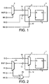
- the scan latch 1 consists of a two input multiplexer 2 having a first input 10 and a second input 11 and further having a control input 12.
- the multiplexer output is connected to the input of latch circuitry 3, here shown figuratively as a single flip flop.
- An input multiplexer 4 has an output terminal connected to the first input 10 of the scan latch and further has two inputs D and BIST as well as a control input BE.
- the second input 11 of the scan latch is provided at an input terminal (SI) and the control input at an input terminal (SE).
- the circuitry of Figure 1 is connected to memory circuitry and has three modes of operation, a normal mode in which the memory is addressed in a conventional way to provide a data output connected to terminal D, a scan mode in which data are scanned through the memory and the output provided at the terminal (SI) and a third built-in self-test mode in which the configuration of the memory is set, together with external circuitry to cause the memory to cycle through all the possible states of the memory.
- the input terminal (BE) BIST enable
- SE input to terminal
- the input multiplexer 4 connects the D input (memory data) to the first input terminal 10 of the scan latch and the multiplexer 2 of the scan latch connects the first input 10 to the latch circuitry 3.
- signal (BE) is set to logical 1
- signal (SE) is set to logical 0.
- the built-in self-test input (BIST) is connected by the input multiplexer 4 to the first input terminal 10 of the scan latch, the multiplexer 2 continuing to supply the first input 10 to the latch circuitry 3.
- the scan enable signal (SE) is set to logical 1 and the second input 11 which receives the scan input from the memory is connected by the multiplexer 2 to the latch circuitry 3.
- the scan latch circuitry of the present invention connects the data input terminal D directly to the first input terminal 10 of the scan latch 1.
- the second input terminal 11 of the scan latch 1 is derived from the output of a two-input multiplexer 24, the two inputs to the multiplexer being derived from the built-in self-test (BIST) and the scan input data signal (SI).
- the two-input multiplexer 24 is controlled by the scan enable signal (SE).
- the control input 12 of the scan latch is provided by the output of the two input OR gate 25 whose inputs are provided by the BIST enable signal (BE) and the scan enable signal (SE).
- control input 12 of the scan latch 1 is at logical 0 and the data input D of the memory is connected via the multiplexer 2 of the scan latch to the latch circuitry 3 of the scan latch.
- the input multiplexer 24 connects the second input (SI) to the second input 11 of the scan latch and thus to the latch circuitry 3. Only if the BIST enable signal (BE) is at logical 1 and the scan enable signal (SE) as at logic 0 is the BIST data signal BIST connected by the input multiplexer 24 to the second input 11 of the scan latch, and thus to the latch circuitry 3 of the scan latch.
- this arrangement is advantageous in that the data input to the scan latch, which is critical path for normal operation, is not impeded by passage through a multiplexer or by gating circuitry.
- the arrangement is disadvantageous in that an additional gate 25 is required by comparison with the conventional circuit but it will be understood by those skilled in the art that for a conventional memory arrangement there will be a scan latch for each bit (e.g. 32 bits) of the memory and that the gate 25 is shared between all of the scan latches.
Landscapes
- Engineering & Computer Science (AREA)
- General Engineering & Computer Science (AREA)
- Physics & Mathematics (AREA)
- General Physics & Mathematics (AREA)
- Tests Of Electronic Circuits (AREA)
Abstract
Description
As has previously been discussed, the circuitry shown in Figure 1 is disadvantageous in that the data input D from the memory suffers undesirable delay.
Claims (8)
- A scan latch circuit for a circuit having a data output and first and second outputs for test information, the scan latch circuit comprising a scan latch having first and second inputs and a control input for selecting between said first and second inputs for input to latch circuitry of said scan latch, the circuit further having first and second select signal inputs for selecting first and second test modes in which a respective one of said first and second test information is passed to said latch circuitry, wherein said data output is connected directly to one of said first and second inputs of said scan latch, and wherein said first and second outputs and said first and second select signals are connected by further circuitry to said control and said other input of said scan latch.
- A scan latch circuit as claimed in claim 1 wherein said further circuitry comprises a two input multiplexer having one input connected to receive said first output, the other input of said two input multiplexer being connected to receive said second output, the select terminal of said multiplexer being connected to receive one of said first and second select signals.
- A scan latch circuit as claimed in claim 2 wherein said first and second select signals are connected to the control input of said scan latch via an OR gate whereby said control input responds to the logical OR of said select signals.
- The combination of a circuit having a data output and first and second outputs for test information with a scan latch circuit, the scan latch circuit comprising a scan latch having first and second inputs and a control input for selecting between said first and second inputs for input to latch circuitry of said scan latch, the scan latch circuit further having first and second select signal inputs for selecting first and second test modes in which a respective one of said first and second test information is passed to said latch circuitry, wherein said data output is connected directly to one of said first and second inputs of said scan latch, and wherein said first and second outputs and said first and second select signals are connected by further circuitry to said control and said other input of said scan latch.
- The combination of claim 4, wherein said further circuitry comprises a two input multiplexer having one input connected to receive said first output, the other input of said two input multiplexer being connected to receive said second output, the select terminal of said multiplexer being connected to receive one of said first and second select signals.
- The combination of claim 5 wherein said first and second select signals are connected to the control input of said scan latch via an OR gate whereby said control input responds to the logical OR of said select signals.
- The combination of any one of claims 4-6 wherein said circuit comprises a memory.
- The combination of any one of claims 4-7 wherein said first and second test modes are respectively scan and built-in self-test modes, and said first and second signals are respectively scan and built-in self-test enable signals
Applications Claiming Priority (2)
| Application Number | Priority Date | Filing Date | Title |
|---|---|---|---|
| GB9920077 | 1999-08-24 | ||
| GBGB9920077.6A GB9920077D0 (en) | 1999-08-24 | 1999-08-24 | Scan latch circuit |
Publications (2)
| Publication Number | Publication Date |
|---|---|
| EP1081498A1 true EP1081498A1 (en) | 2001-03-07 |
| EP1081498B1 EP1081498B1 (en) | 2006-08-02 |
Family
ID=10859747
Family Applications (1)
| Application Number | Title | Priority Date | Filing Date |
|---|---|---|---|
| EP00302835A Expired - Lifetime EP1081498B1 (en) | 1999-08-24 | 2000-04-04 | Scan latch circuit |
Country Status (4)
| Country | Link |
|---|---|
| US (1) | US6622273B1 (en) |
| EP (1) | EP1081498B1 (en) |
| DE (1) | DE60029705D1 (en) |
| GB (1) | GB9920077D0 (en) |
Families Citing this family (19)
| Publication number | Priority date | Publication date | Assignee | Title |
|---|---|---|---|---|
| US7246287B1 (en) * | 2002-04-04 | 2007-07-17 | Mips Technologies, Inc. | Full scan solution for latched-based design |
| WO2004073041A2 (en) * | 2003-02-13 | 2004-08-26 | Mentor Graphics Corporation | Testing embedded memories in an integrated circuit |
| KR20050039256A (en) * | 2003-10-24 | 2005-04-29 | 삼성전자주식회사 | Scan test device |
| US7842948B2 (en) * | 2004-02-27 | 2010-11-30 | Nvidia Corporation | Flip chip semiconductor die internal signal access system and method |
| US7313744B2 (en) * | 2004-02-27 | 2007-12-25 | International Business Machines Corporation | Methods and apparatus for testing a scan chain to isolate defects |
| KR101076809B1 (en) * | 2004-06-18 | 2011-10-25 | 삼성전자주식회사 | Scan flip-flop circuit to reduce redundant power consumption |
| US7279887B1 (en) * | 2004-08-06 | 2007-10-09 | Nvidia Corporation | In-process system level test before surface mount |
| US7272761B2 (en) * | 2004-11-04 | 2007-09-18 | International Business Machines Corporation | Method, system, and program product for controlling test data of a logic built-in self-test of an integrated circuit |
| US7237163B2 (en) * | 2004-11-05 | 2007-06-26 | International Business Machines Corporation | Leakage current reduction system and method |
| US8051350B2 (en) * | 2004-11-09 | 2011-11-01 | Via Technologies Inc. | Serial interface device built-in self test |
| TWI273259B (en) * | 2004-11-09 | 2007-02-11 | Via Tech Inc | Built-in test architecture |
| US7640475B2 (en) * | 2006-03-30 | 2009-12-29 | Texas Instruments Incorporated | At-speed transition fault testing with low speed scan enable |
| US7707466B2 (en) * | 2007-02-23 | 2010-04-27 | Freescale Semiconductor, Inc. | Shared latch for memory test/repair and functional operations |
| US8065647B2 (en) * | 2007-10-19 | 2011-11-22 | The University Of Utah Research Foundation | Method and system for asynchronous chip design |
| US8271252B2 (en) * | 2007-11-08 | 2012-09-18 | Nvidia Corporation | Automatic verification of device models |
| US8510616B2 (en) * | 2008-02-14 | 2013-08-13 | Nvidia Corporation | Scalable scan-based test architecture with reduced test time and test power |
| US8745200B2 (en) * | 2008-05-06 | 2014-06-03 | Nvidia Corporation | Testing operation of processors setup to operate in different modes |
| US8943457B2 (en) * | 2008-11-24 | 2015-01-27 | Nvidia Corporation | Simulating scan tests with reduced resources |
| US11017135B2 (en) | 2015-11-24 | 2021-05-25 | Microchip Technology Incorporated | Scan logic for circuit designs with latches and flip-flops |
Citations (2)
| Publication number | Priority date | Publication date | Assignee | Title |
|---|---|---|---|---|
| US4740970A (en) * | 1985-01-17 | 1988-04-26 | Plessey Overseas Limited | Integrated circuit arrangement |
| EP0822497A2 (en) * | 1996-04-09 | 1998-02-04 | Texas Instruments Incorporated | Boundary scan cell |
Family Cites Families (9)
| Publication number | Priority date | Publication date | Assignee | Title |
|---|---|---|---|---|
| US5319646A (en) * | 1991-09-18 | 1994-06-07 | Ncr Corporation | Boundary-scan output cell with non-critical enable path |
| JPH05232196A (en) * | 1992-02-25 | 1993-09-07 | Mitsubishi Electric Corp | Test circuit |
| US5592493A (en) * | 1994-09-13 | 1997-01-07 | Motorola Inc. | Serial scan chain architecture for a data processing system and method of operation |
| US5574731A (en) * | 1995-02-22 | 1996-11-12 | National Semiconductor Corporation | Set/reset scan flip-flops |
| US5825785A (en) * | 1996-05-24 | 1998-10-20 | Internaitonal Business Machines Corporation | Serial input shift register built-in self test circuit for embedded circuits |
| US6158032A (en) * | 1998-03-27 | 2000-12-05 | International Business Machines Corporation | Data processing system, circuit arrangement and program product including multi-path scan interface and methods thereof |
| US6185710B1 (en) * | 1998-03-30 | 2001-02-06 | International Business Machines Corporation | High-performance IEEE1149.1-compliant boundary scan cell |
| US6195775B1 (en) * | 1998-09-02 | 2001-02-27 | International Business Machines Corporation | Boundary scan latch configuration for generalized scan designs |
| US6393592B1 (en) * | 1999-05-21 | 2002-05-21 | Adaptec, Inc. | Scan flop circuitry and methods for making the same |
-
1999
- 1999-08-24 GB GBGB9920077.6A patent/GB9920077D0/en not_active Ceased
-
2000
- 2000-04-04 EP EP00302835A patent/EP1081498B1/en not_active Expired - Lifetime
- 2000-04-04 DE DE60029705T patent/DE60029705D1/en not_active Expired - Lifetime
- 2000-04-11 US US09/546,752 patent/US6622273B1/en not_active Expired - Lifetime
Patent Citations (2)
| Publication number | Priority date | Publication date | Assignee | Title |
|---|---|---|---|---|
| US4740970A (en) * | 1985-01-17 | 1988-04-26 | Plessey Overseas Limited | Integrated circuit arrangement |
| EP0822497A2 (en) * | 1996-04-09 | 1998-02-04 | Texas Instruments Incorporated | Boundary scan cell |
Also Published As
| Publication number | Publication date |
|---|---|
| US6622273B1 (en) | 2003-09-16 |
| DE60029705D1 (en) | 2006-09-14 |
| EP1081498B1 (en) | 2006-08-02 |
| GB9920077D0 (en) | 1999-10-27 |
Similar Documents
| Publication | Publication Date | Title |
|---|---|---|
| US6622273B1 (en) | Scan latch circuit | |
| US5352940A (en) | Ram convertible look-up table based macrocell for PLDs | |
| US6191603B1 (en) | Modular embedded test system for use in integrated circuits | |
| US4841233A (en) | Semiconductor integrated circuit adapted to carry out operation test | |
| US7046035B2 (en) | Programmable driver for an I/O pin of an integrated circuit | |
| US5260948A (en) | Bidirectional boundary-scan circuit | |
| US4855958A (en) | Semiconductor integrated circuit device having logic macro and random access memory macro | |
| US20090115453A1 (en) | Ic output signal path with switch, bus holder, and buffer | |
| KR100303618B1 (en) | Fully testable chip with self-timed memory array | |
| US20140215282A1 (en) | 1149.1 tap linking modules | |
| EP0758113B1 (en) | Test mode matrix circuit for an embedded microprocessor core | |
| US6873197B2 (en) | Scan flip-flop circuit capable of guaranteeing normal operation | |
| JP2000002754A (en) | Scan flip-flop circuit | |
| US5384533A (en) | Testing method, testing circuit and semiconductor integrated circuit having testing circuit | |
| US5109383A (en) | Scan path circuit | |
| US5406567A (en) | Off-line test circuit of a semiconnector integrated logic circuit | |
| JPH08278840A (en) | Keeper circuit for three-state bus and integrated circuit containing it | |
| US5347520A (en) | Boundary-scan enable cell with non-critical enable path | |
| US6327683B1 (en) | Device scan testing | |
| US5936976A (en) | Selecting a test data input bus to supply test data to logical blocks within an integrated circuit | |
| HK6793A (en) | Integrated semiconducteur memory | |
| US4766593A (en) | Monolithically integrated testable registers that cannot be directly addressed | |
| EP1061375B1 (en) | Semiconductor device including macros and its testing method | |
| US7746140B2 (en) | Scannable latch | |
| US20030226079A1 (en) | Scan-path flip-flop circuit for integrated circuit memory |
Legal Events
| Date | Code | Title | Description |
|---|---|---|---|
| PUAI | Public reference made under article 153(3) epc to a published international application that has entered the european phase |
Free format text: ORIGINAL CODE: 0009012 |
|
| AK | Designated contracting states |
Kind code of ref document: A1 Designated state(s): AT BE CH CY DE DK ES FI FR GB GR IE IT LI LU MC NL PT SE |
|
| AX | Request for extension of the european patent |
Free format text: AL;LT;LV;MK;RO;SI |
|
| 17P | Request for examination filed |
Effective date: 20010906 |
|
| AKX | Designation fees paid |
Free format text: DE FR GB IT |
|
| 17Q | First examination report despatched |
Effective date: 20040521 |
|
| GRAP | Despatch of communication of intention to grant a patent |
Free format text: ORIGINAL CODE: EPIDOSNIGR1 |
|
| GRAS | Grant fee paid |
Free format text: ORIGINAL CODE: EPIDOSNIGR3 |
|
| GRAA | (expected) grant |
Free format text: ORIGINAL CODE: 0009210 |
|
| AK | Designated contracting states |
Kind code of ref document: B1 Designated state(s): DE FR GB IT |
|
| PG25 | Lapsed in a contracting state [announced via postgrant information from national office to epo] |
Ref country code: IT Free format text: LAPSE BECAUSE OF FAILURE TO SUBMIT A TRANSLATION OF THE DESCRIPTION OR TO PAY THE FEE WITHIN THE PRESCRIBED TIME-LIMIT;WARNING: LAPSES OF ITALIAN PATENTS WITH EFFECTIVE DATE BEFORE 2007 MAY HAVE OCCURRED AT ANY TIME BEFORE 2007. THE CORRECT EFFECTIVE DATE MAY BE DIFFERENT FROM THE ONE RECORDED. Effective date: 20060802 |
|
| REG | Reference to a national code |
Ref country code: GB Ref legal event code: FG4D |
|
| REF | Corresponds to: |
Ref document number: 60029705 Country of ref document: DE Date of ref document: 20060914 Kind code of ref document: P |
|
| PG25 | Lapsed in a contracting state [announced via postgrant information from national office to epo] |
Ref country code: DE Free format text: LAPSE BECAUSE OF FAILURE TO SUBMIT A TRANSLATION OF THE DESCRIPTION OR TO PAY THE FEE WITHIN THE PRESCRIBED TIME-LIMIT Effective date: 20061103 |
|
| ET | Fr: translation filed | ||
| PLBE | No opposition filed within time limit |
Free format text: ORIGINAL CODE: 0009261 |
|
| STAA | Information on the status of an ep patent application or granted ep patent |
Free format text: STATUS: NO OPPOSITION FILED WITHIN TIME LIMIT |
|
| 26N | No opposition filed |
Effective date: 20070503 |
|
| PGFP | Annual fee paid to national office [announced via postgrant information from national office to epo] |
Ref country code: FR Payment date: 20070426 Year of fee payment: 8 |
|
| REG | Reference to a national code |
Ref country code: FR Ref legal event code: ST Effective date: 20081231 |
|
| PG25 | Lapsed in a contracting state [announced via postgrant information from national office to epo] |
Ref country code: FR Free format text: LAPSE BECAUSE OF NON-PAYMENT OF DUE FEES Effective date: 20080430 |
|
| PGFP | Annual fee paid to national office [announced via postgrant information from national office to epo] |
Ref country code: GB Payment date: 20140327 Year of fee payment: 15 |
|
| GBPC | Gb: european patent ceased through non-payment of renewal fee |
Effective date: 20150404 |
|
| PG25 | Lapsed in a contracting state [announced via postgrant information from national office to epo] |
Ref country code: GB Free format text: LAPSE BECAUSE OF NON-PAYMENT OF DUE FEES Effective date: 20150404 |