EP1079524A1 - CMOS switching circuitry - Google Patents
CMOS switching circuitry Download PDFInfo
- Publication number
- EP1079524A1 EP1079524A1 EP00303948A EP00303948A EP1079524A1 EP 1079524 A1 EP1079524 A1 EP 1079524A1 EP 00303948 A EP00303948 A EP 00303948A EP 00303948 A EP00303948 A EP 00303948A EP 1079524 A1 EP1079524 A1 EP 1079524A1
- Authority
- EP
- European Patent Office
- Prior art keywords
- output
- circuit
- terminal
- input
- circuitry
- Prior art date
- Legal status (The legal status is an assumption and is not a legal conclusion. Google has not performed a legal analysis and makes no representation as to the accuracy of the status listed.)
- Granted
Links
- 230000000295 complement effect Effects 0.000 claims description 3
- 238000006880 cross-coupling reaction Methods 0.000 description 1
- 238000010586 diagram Methods 0.000 description 1
- 238000005516 engineering process Methods 0.000 description 1
- 230000003068 static effect Effects 0.000 description 1
- 230000007704 transition Effects 0.000 description 1
Images
Classifications
-
- H—ELECTRICITY
- H03—ELECTRONIC CIRCUITRY
- H03K—PULSE TECHNIQUE
- H03K3/00—Circuits for generating electric pulses; Monostable, bistable or multistable circuits
- H03K3/02—Generators characterised by the type of circuit or by the means used for producing pulses
- H03K3/353—Generators characterised by the type of circuit or by the means used for producing pulses by the use, as active elements, of field-effect transistors with internal or external positive feedback
- H03K3/356—Bistable circuits
- H03K3/356104—Bistable circuits using complementary field-effect transistors
- H03K3/356113—Bistable circuits using complementary field-effect transistors using additional transistors in the input circuit
- H03K3/356121—Bistable circuits using complementary field-effect transistors using additional transistors in the input circuit with synchronous operation
-
- H—ELECTRICITY
- H03—ELECTRONIC CIRCUITRY
- H03K—PULSE TECHNIQUE
- H03K3/00—Circuits for generating electric pulses; Monostable, bistable or multistable circuits
- H03K3/02—Generators characterised by the type of circuit or by the means used for producing pulses
- H03K3/353—Generators characterised by the type of circuit or by the means used for producing pulses by the use, as active elements, of field-effect transistors with internal or external positive feedback
- H03K3/356—Bistable circuits
- H03K3/356104—Bistable circuits using complementary field-effect transistors
- H03K3/356182—Bistable circuits using complementary field-effect transistors with additional means for controlling the main nodes
- H03K3/356191—Bistable circuits using complementary field-effect transistors with additional means for controlling the main nodes with synchronous operation
Definitions
- the present invention relates to CMOS switching circuitry, and more specifically but not exclusively to CMOS level shift circuitry.
- level shift circuitry providing an output at a different voltage level to the input.
- a difficulty may arise in that the relative current carrying ability of the p FETs and n FETs may vary from chip-to-chip.
- the level shifting circuitry requires a particular relationship between p FETs and n FETs to operate properly, difficulties may arise. For example, where the pull-up of an output node is provided by a p FET and the pull-down by an n FET the circuit may operate too slowly under certain tolerance conditions.
- a CMOS switching circuit comprising input circuitry and output circuitry, said input circuitry having a first input switch and a second input switch, each input switch being connected to an input terminal, a pair of cross-coupled CMOS inverters forming bistable circuitry, said bistable circuitry connectable to a power terminal and having a first and a second branch, said first branch being connectable to a reference terminal via said first input switch and said second branch being connectable to said reference terminal via said second input switch, said output circuitry being connected to said bistable circuitry for providing a circuit output.
- said first input switch has a control node coupled directly to said input terminal and said second switch has a control node coupled to said input terminal via a first inverter, whereby drive to said input switches is complementary.
- each of said CMOS inverters has a respective common gate, the common gate of the CMOS inverter of the first branch and the common gate of the CMOS inverter of the second branch being connected to said output circuitry.
- the two CMOS inverters have a common source terminal connectable to said power terminal via a power switch.
- said power switch is a p FET.
- the output circuitry comprises an output p FET having a gate coupled to the common gate of said CMOS inverter of the first branch via a further inverter, and an output n FET having a gate coupled to the common gate of said CMOS inverter of the second branch, the output p FET and the output n FET having a common source/drain terminal.
- the common gates of the CMOS inverters of said first and second branches are connected to said reference terminal via respective equalization switches.
- said common source/drain terminal is connected to a circuit output terminal via cross-coupled output inverters.
- the cross-coupled output inverters comprise a forward inverter and a relatively weak feedback inverter.
- the power switch has a control node connected in common with the control nodes of the equalization switches.
- a voltage supply to said input circuitry differs from a voltage supply to said output circuitry whereby said circuit output is level shifted.
- a level shifting flip-flop 1 consists of a first input switch 11, which is an n FET having a source terminal connected to a reference voltage 45 and a gate terminal connected to an input terminal 30, and a second input switch 21, which is likewise an n FET having a source terminal connected to a first negative supply terminal 45.
- the second input switch 21 has a control gate coupled to the input terminal 30 via an input inverter 31 so that the drive to the input switches is complementary whereby one input switch is on, the other is off.
- the first input switch 11 further has a drain node connected to a circuit node 41 via a first CMOS inverter 10 while the second input switch 21 has a drain node connected to the circuit node 41 via a second CMOS inverter 20.
- the first CMOS inverter 10 consists of an n FET 13 having a source/drain terminal connected to the drain of the first input switch 20, a drain/source terminal connected to a drain/source terminal of a p FET 12, which has a source/drain terminal connected to the circuit node 41.
- the gates of the p and n FETs 12, 13 of the first CMOS inverter 10 are connected in common at a first gate node 15.
- the second CMOS inverter consists of an n FET 23 having a source/drain terminal connected to the drain terminal of the second input transistor 21, and a drain/source terminal connected to a drain/source terminal of a p FET 22, which in turn has a source/drain terminal connected to the circuit node 41.
- the gates of the p and n FETs 22, 23 of the second CMOS inverter 20 are connected in common at a second gate terminal 14.
- the first gate terminal 15 is further connected to the common source/drain terminals of the second CMOS inverter 20 and the second gate terminal 14 is connected to the common source/drain terminals of the first CMOS inverter 10.
- the first gate terminal 15 is also connected directly to the gate of an output n FET 55, which has a source terminal connected to a second negative supply terminal 47, and a drain terminal.
- the second gate terminal 14 is connected via a further inverter 56 to the gate of an output p FET 54 having a source connected to a supply terminal 46 and a drain connected to the drain of the output n FET 55.
- the common terminal of the output p and n FETs is connected to an output terminal 60 via an output inverter 51 which comprises a forward inverter 53 and a feedback inverter 52, the feedback inverter 52 being weak by comparison with the forward inverter 53.
- the first gate terminal 15 is connectable to the reference terminal via a first equalization transistor 58, which is an n FET and the second gate terminal 14 is connectable to a third negative supply terminal 48 via a second equalization transistor 57, which is a similar n FET.
- the two equalization transistors have a common control node 59.
- the circuit node 41 is connectable to a second power supply terminal 43 via a power supply switch 42, in the form of a p FET having a source/drain terminal connected to the power supply terminal and a drain/source terminal connected to the circuit node 41.
- the gate of the power supply switch is connected to a clock terminal 44.
- the power supply modes 43 and 46 are typically supplied with diferent positive supply voltage, with the negative supply modes being connected in common.
- the first negative supply mode 45 may be at a different potential to the second and third modes 47, 48.
- the clock terminal 44 and the equalization transistor control terminal 59 are supplied with a clock signal such that while the clock is at a logic low the circuit 1 is active and while the clock is at a logic high the circuit 1 is inactive.
- With the clock at a logic low, (circuit active) assume that the first gate terminal 15 is at a high potential. Due to the cross-coupling of the two CMOS inverters 10, 20 this means that the second gate terminal 14 is at a low potential with the n FET 13 of the first inverter in a conductive condition and the p FET 22 of the second inverter likewise in a conductive condition. Thus, the output n FET 55 will be on and the output p FET 54 will be off. Hence the output node 60 will be high.
- This condition corresponds to the input terminal 30 being at a high potential which causes the first input switch 11 to be conductive and the second input switch 21 to be non conductive.
- the input terminal changes to a low potential, this causes the first input switch 11 to be rendered non-conductive and the second input switch 21 to be rendered conductive. Then, when the clock signal once again assumes its logic low state, the circuit node 41 becomes again connected to the power supply terminal 43 and the equalization transistors 57 and 58 turn off.
- the "off" state of the first input switch 11 means that the first inverter 10 is pulled up towards the positive supply and the common node between the p transistor 12 and the n transistor 13 goes high. This node is connected to the second gate terminal 14 of the second CMOS inverter 20 which is in turn being connected to the reference terminal 45 via the on second switch 21.
- the n transistor 23 of the second CMOS inverter 20 turns on which in turn positively pulls the first gate terminal 15 of the first inverter to a low level, turning on the p FET 12 of the CMOS inverter 10.
- the application of a low potential at the first gate terminal 15 to the output circuit causes the output n transistor 55 to turn off.
- the application of a high potential at the second gate terminal 14 causes, via the inverter 56, a low potential to be applied to the p output FET 54 which then turns on pulling the common output node of the output inverter high to the potential on the supply terminal 46, and causing the output terminal via the latch 51 to go low.
- the clock signal goes to a logic high state isolating the common node 41 from the power supply terminal 43 and equalizing the potential at the gate terminals 14 and 15 to the reference level at mode 48.
- the output inverter again goes to a tristate and the output terminal 60 remains at an unchanged potential.
Landscapes
- Logic Circuits (AREA)
Abstract
Description
- The present invention relates to CMOS switching circuitry, and more specifically but not exclusively to CMOS level shift circuitry.
- The art is replete with level shift circuitry providing an output at a different voltage level to the input.
- In an integrated circuit using CMOS technology it is desirable to use p FETs and n FETS. A difficulty may arise in that the relative current carrying ability of the p FETs and n FETs may vary from chip-to-chip. Where the level shifting circuitry requires a particular relationship between p FETs and n FETs to operate properly, difficulties may arise. For example, where the pull-up of an output node is provided by a p FET and the pull-down by an n FET the circuit may operate too slowly under certain tolerance conditions.
- It is accordingly an object of the present invention to at least partially mitigate the difficulties of the prior art.
- According to a first aspect of the present invention there is provided a CMOS switching circuit comprising input circuitry and output circuitry, said input circuitry having a first input switch and a second input switch, each input switch being connected to an input terminal, a pair of cross-coupled CMOS inverters forming bistable circuitry, said bistable circuitry connectable to a power terminal and having a first and a second branch, said first branch being connectable to a reference terminal via said first input switch and said second branch being connectable to said reference terminal via said second input switch, said output circuitry being connected to said bistable circuitry for providing a circuit output.
- Preferably said first input switch has a control node coupled directly to said input terminal and said second switch has a control node coupled to said input terminal via a first inverter, whereby drive to said input switches is complementary.
- Advantageously each of said CMOS inverters has a respective common gate, the common gate of the CMOS inverter of the first branch and the common gate of the CMOS inverter of the second branch being connected to said output circuitry.
- Conveniently the two CMOS inverters have a common source terminal connectable to said power terminal via a power switch.
- Advantageously said power switch is a p FET.
- Advantageously the output circuitry comprises an output p FET having a gate coupled to the common gate of said CMOS inverter of the first branch via a further inverter, and an output n FET having a gate coupled to the common gate of said CMOS inverter of the second branch, the output p FET and the output n FET having a common source/drain terminal.
- Preferably the common gates of the CMOS inverters of said first and second branches are connected to said reference terminal via respective equalization switches.
- Advantageously said common source/drain terminal is connected to a circuit output terminal via cross-coupled output inverters.
- Conveniently the cross-coupled output inverters comprise a forward inverter and a relatively weak feedback inverter.
- Conveniently the power switch has a control node connected in common with the control nodes of the equalization switches.
- Preferably a voltage supply to said input circuitry differs from a voltage supply to said output circuitry whereby said circuit output is level shifted.
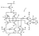
- An embodiment of the invention will now be described, by way of example only, with reference to the accompanying drawing which shows a schematic diagram of an embodiment of a CMOS switching circuit in accordance with the invention.
- A level shifting flip-flop 1 consists of a
first input switch 11, which is an n FET having a source terminal connected to areference voltage 45 and a gate terminal connected to aninput terminal 30, and asecond input switch 21, which is likewise an n FET having a source terminal connected to a firstnegative supply terminal 45. Thesecond input switch 21 has a control gate coupled to theinput terminal 30 via aninput inverter 31 so that the drive to the input switches is complementary whereby one input switch is on, the other is off. Thefirst input switch 11 further has a drain node connected to acircuit node 41 via afirst CMOS inverter 10 while thesecond input switch 21 has a drain node connected to thecircuit node 41 via asecond CMOS inverter 20. Thefirst CMOS inverter 10 consists of ann FET 13 having a source/drain terminal connected to the drain of thefirst input switch 20, a drain/source terminal connected to a drain/source terminal ofa p FET 12, which has a source/drain terminal connected to thecircuit node 41. The gates of the p andn FETs first CMOS inverter 10 are connected in common at afirst gate node 15. - Similarly, the second CMOS inverter consists of an
n FET 23 having a source/drain terminal connected to the drain terminal of thesecond input transistor 21, and a drain/source terminal connected to a drain/source terminal ofa p FET 22, which in turn has a source/drain terminal connected to thecircuit node 41. The gates of the p andn FETs second CMOS inverter 20 are connected in common at asecond gate terminal 14. - The
first gate terminal 15 is further connected to the common source/drain terminals of thesecond CMOS inverter 20 and thesecond gate terminal 14 is connected to the common source/drain terminals of thefirst CMOS inverter 10. - The
first gate terminal 15 is also connected directly to the gate of an output n FET 55, which has a source terminal connected to a secondnegative supply terminal 47, and a drain terminal. Thesecond gate terminal 14 is connected via afurther inverter 56 to the gate of an output p FET 54 having a source connected to a supply terminal 46 and a drain connected to the drain of theoutput n FET 55. The common terminal of the output p and n FETs is connected to anoutput terminal 60 via anoutput inverter 51 which comprises aforward inverter 53 and afeedback inverter 52, thefeedback inverter 52 being weak by comparison with theforward inverter 53. - The
first gate terminal 15 is connectable to the reference terminal via afirst equalization transistor 58, which is an n FET and thesecond gate terminal 14 is connectable to a thirdnegative supply terminal 48 via asecond equalization transistor 57, which is a similar n FET. The two equalization transistors have acommon control node 59. - The
circuit node 41 is connectable to a secondpower supply terminal 43 via apower supply switch 42, in the form of a p FET having a source/drain terminal connected to the power supply terminal and a drain/source terminal connected to thecircuit node 41. The gate of the power supply switch is connected to aclock terminal 44. - The operation of the circuit 1 will now be described:-
- To provide level shifting, the
power supply modes 43 and 46 are typically supplied with diferent positive supply voltage, with the negative supply modes being connected in common. Alternatively, or as well, the firstnegative supply mode 45 may be at a different potential to the second andthird modes - The
clock terminal 44 and the equalizationtransistor control terminal 59 are supplied with a clock signal such that while the clock is at a logic low the circuit 1 is active and while the clock is at a logic high the circuit 1 is inactive. With the clock at a logic low, (circuit active) assume that thefirst gate terminal 15 is at a high potential. Due to the cross-coupling of the twoCMOS inverters second gate terminal 14 is at a low potential with then FET 13 of the first inverter in a conductive condition and thep FET 22 of the second inverter likewise in a conductive condition. Thus, theoutput n FET 55 will be on and theoutput p FET 54 will be off. Hence theoutput node 60 will be high. - This condition corresponds to the
input terminal 30 being at a high potential which causes thefirst input switch 11 to be conductive and thesecond input switch 21 to be non conductive. - When the clock pulse makes its transition to a logic high state the
circuit node 41 becomes disconnected from the power supply atmode 43 and theequalization transistors 57 an 58 are turned on thus supplying an off signal to both the p andn output FETs output terminal 60 remains in its previous state. - If the input terminal changes to a low potential, this causes the
first input switch 11 to be rendered non-conductive and thesecond input switch 21 to be rendered conductive. Then, when the clock signal once again assumes its logic low state, thecircuit node 41 becomes again connected to thepower supply terminal 43 and theequalization transistors first input switch 11 means that thefirst inverter 10 is pulled up towards the positive supply and the common node between thep transistor 12 and then transistor 13 goes high. This node is connected to thesecond gate terminal 14 of thesecond CMOS inverter 20 which is in turn being connected to thereference terminal 45 via the onsecond switch 21. The result is that then transistor 23 of thesecond CMOS inverter 20 turns on which in turn positively pulls thefirst gate terminal 15 of the first inverter to a low level, turning on thep FET 12 of theCMOS inverter 10.
The application of a low potential at thefirst gate terminal 15 to the output circuit causes theoutput n transistor 55 to turn off. The application of a high potential at thesecond gate terminal 14 causes, via theinverter 56, a low potential to be applied to thep output FET 54 which then turns on pulling the common output node of the output inverter high to the potential on the supply terminal 46, and causing the output terminal via thelatch 51 to go low. - Once again the clock signal goes to a logic high state isolating the
common node 41 from thepower supply terminal 43 and equalizing the potential at thegate terminals mode 48. The output inverter again goes to a tristate and theoutput terminal 60 remains at an unchanged potential. - When the
input terminal 30 is again at logic high theinput switch 11 will be turned on and thesecond input switch 21 will be turned on and when the clock signal returns to its logic low state,transistor 13 will turn on during thesecond gate 14 low, turning thep FET 22 of the second CMOS inverter on so that the above-described first state will pertain. - From a review of the above description of operation it will be seen that at no stage is the relative current carrying capability of PMOS and NMOS transistors compared. Moreover, there is no static flow of current at any time.
Claims (11)
- A CMOS switching circuit comprising input circuitry and output circuitry, said input circuitry having a first input switch and a second input switch, each input switch being connected to an input terminal, a pair of cross-coupled CMOS inverters forming bistable circuitry, said bistable circuitry connectable to a power terminal and having a first and a second branch, said first branch being connectable to a reference terminal via said first input switch and said second branch being connectable to said reference terminal via said second input switch, said output circuitry being connected to said bistable circuitry for providing a circuit output.
- A circuit as claimed in claim 1 wherein said first input switch has a control node coupled directly to said input terminal and said second switch has a control node coupled to said input terminal via a first inverter, whereby drive to said input switches is complementary.
- A circuit as claimed in claim 2 wherein each of said CMOS inverters has a respective common gate, the common gate of the CMOS inverter of the first branch and the common gate of the CMOS inverter of the second branch being connected to said output circuitry.
- A circuit as claimed in claim 3 wherein the two CMOS inverters have a common source terminal connectable to said power terminal via a power switch.
- A circuit as claimed in claim 4 wherein said power switch is a p FET.
- A circuit as claimed in any preceding claim wherein the output circuitry comprises an output p FET having a gate coupled to the common gate of said CMOS inverter of the first branch via a further inverter, and an output n FET having a gate coupled to the common gate of said CMOS inverter of the second branch, the output p FET and the output n FET having a common source/drain terminal.
- A circuit as claimed in claim 6 the common gates of the CMOS inverters of said first and second branches are connected to said reference terminal via respective equalization switches.
- A circuit as claimed in claim 6 or 7 wherein said common source/drain terminal is connected to a circuit output terminal via cross-coupled output inverters.
- A circuit as claimed in claim 8 wherein the cross-coupled output inverters comprise a forward inverter and a relatively weak feedback inverter.
- A circuit as claimed in claims 7, 8 or 9 the power switch has a control node connected in common with the control nodes of the equalization switches.
- A circuit as claimed in any preceding claim wherein a voltage supply to said input circuitry differs from a voltage supply to said output circuitry whereby said circuit output is level shifted.
Applications Claiming Priority (2)
| Application Number | Priority Date | Filing Date | Title |
|---|---|---|---|
| GBGB9920172.5A GB9920172D0 (en) | 1999-08-25 | 1999-08-25 | Cmos switching cicuitry |
| GB9920172 | 1999-08-25 |
Publications (2)
| Publication Number | Publication Date |
|---|---|
| EP1079524A1 true EP1079524A1 (en) | 2001-02-28 |
| EP1079524B1 EP1079524B1 (en) | 2006-08-16 |
Family
ID=10859814
Family Applications (1)
| Application Number | Title | Priority Date | Filing Date |
|---|---|---|---|
| EP00303948A Expired - Lifetime EP1079524B1 (en) | 1999-08-25 | 2000-05-10 | CMOS switching circuitry |
Country Status (4)
| Country | Link |
|---|---|
| US (1) | US6369632B1 (en) |
| EP (1) | EP1079524B1 (en) |
| DE (1) | DE60030052D1 (en) |
| GB (1) | GB9920172D0 (en) |
Cited By (3)
| Publication number | Priority date | Publication date | Assignee | Title |
|---|---|---|---|---|
| GB2400247A (en) * | 2003-02-28 | 2004-10-06 | Sun Microsystems Inc | A combined flip-flop and voltage level up-converter for a CMOS IC output circuit |
| DE102006016356A1 (en) * | 2006-04-05 | 2007-10-11 | Micronas Gmbh | Circuit arrangement for glitch-free or glitch-reduced signal transmission between voltage ranges |
| DE102016100044A1 (en) * | 2015-11-16 | 2017-05-18 | Taiwan Semiconductor Manufacturing Company, Ltd. | Level shifter and method |
Families Citing this family (11)
| Publication number | Priority date | Publication date | Assignee | Title |
|---|---|---|---|---|
| US7032146B2 (en) * | 2002-10-29 | 2006-04-18 | International Business Machines Corporation | Boundary scan apparatus and interconnect test method |
| WO2004040765A1 (en) * | 2002-10-31 | 2004-05-13 | Nec Corporation | Level converting circuit |
| JP4128091B2 (en) * | 2003-02-20 | 2008-07-30 | 三洋電機株式会社 | Switch circuit device |
| US7030678B1 (en) * | 2004-02-11 | 2006-04-18 | National Semiconductor Corporation | Level shifter that provides high-speed operation between power domains that have a large voltage difference |
| US7053651B2 (en) * | 2004-09-15 | 2006-05-30 | Avago Technologies General Ip Pte. Ltd. | Low power CMOS switching |
| US20070176666A1 (en) * | 2006-01-30 | 2007-08-02 | Broadcom Corporation | Level translator for adapting a signal to a voltage level |
| WO2007135799A1 (en) * | 2006-05-24 | 2007-11-29 | Sharp Kabushiki Kaisha | Signal processing circuit, level shifter, display panel driving circuit, display device, signal processing circuit |
| US7554860B1 (en) * | 2007-09-21 | 2009-06-30 | Actel Corporation | Nonvolatile memory integrated circuit having assembly buffer and bit-line driver, and method of operation thereof |
| US7772912B2 (en) * | 2007-11-13 | 2010-08-10 | Himax Technologies Limited | Level shift circuit and method thereof |
| KR101020298B1 (en) * | 2009-05-28 | 2011-03-07 | 주식회사 하이닉스반도체 | Level shifter and semiconductor memory device |
| CN118631241B (en) * | 2024-08-09 | 2024-10-29 | 深圳市微源半导体股份有限公司 | Level conversion circuit, switching power supply circuit and electronic equipment |
Citations (5)
| Publication number | Priority date | Publication date | Assignee | Title |
|---|---|---|---|---|
| EP0487911A2 (en) * | 1990-11-29 | 1992-06-03 | International Business Machines Corporation | A fast cycle time clocked amplifier |
| EP0529545A1 (en) * | 1991-08-22 | 1993-03-03 | Sony Corporation | Level shifting CMOS integrated circuits |
| EP0661811A2 (en) * | 1993-12-28 | 1995-07-05 | Oki Electric Industry Co., Ltd. | Level shifter circuit |
| EP0772302A2 (en) * | 1995-10-31 | 1997-05-07 | Hyundai Electronics America, Inc. | Output driver for mixed supply voltage system |
| EP0788235A2 (en) * | 1994-08-10 | 1997-08-06 | Cirrus Logic, Inc. | Digital voltage shifters and systems using the same |
Family Cites Families (6)
| Publication number | Priority date | Publication date | Assignee | Title |
|---|---|---|---|---|
| US5148061A (en) * | 1991-02-27 | 1992-09-15 | Motorola, Inc. | ECL to CMOS translation and latch logic circuit |
| SE9102062D0 (en) | 1991-07-02 | 1991-07-02 | Svenska Toa Throne Ab | PROCEDURES FOR THE MULTIPLE MULTIPLE AND THE MULTIPLE MULTIPLE |
| KR100218336B1 (en) * | 1996-11-28 | 1999-09-01 | 구본준 | Level shifter |
| JP3036481B2 (en) * | 1997-09-16 | 2000-04-24 | 日本電気株式会社 | Level shift circuit |
| US6026011A (en) * | 1998-09-23 | 2000-02-15 | Intel Corporation | CMOS latch design with soft error immunity |
| US6107853A (en) * | 1998-11-09 | 2000-08-22 | Texas Instruments Incorporated | Sense amplifier based flip-flop |
-
1999
- 1999-08-25 GB GBGB9920172.5A patent/GB9920172D0/en not_active Ceased
-
2000
- 2000-05-10 DE DE60030052T patent/DE60030052D1/en not_active Expired - Lifetime
- 2000-05-10 EP EP00303948A patent/EP1079524B1/en not_active Expired - Lifetime
- 2000-08-21 US US09/643,064 patent/US6369632B1/en not_active Expired - Lifetime
Patent Citations (5)
| Publication number | Priority date | Publication date | Assignee | Title |
|---|---|---|---|---|
| EP0487911A2 (en) * | 1990-11-29 | 1992-06-03 | International Business Machines Corporation | A fast cycle time clocked amplifier |
| EP0529545A1 (en) * | 1991-08-22 | 1993-03-03 | Sony Corporation | Level shifting CMOS integrated circuits |
| EP0661811A2 (en) * | 1993-12-28 | 1995-07-05 | Oki Electric Industry Co., Ltd. | Level shifter circuit |
| EP0788235A2 (en) * | 1994-08-10 | 1997-08-06 | Cirrus Logic, Inc. | Digital voltage shifters and systems using the same |
| EP0772302A2 (en) * | 1995-10-31 | 1997-05-07 | Hyundai Electronics America, Inc. | Output driver for mixed supply voltage system |
Non-Patent Citations (1)
| Title |
|---|
| ALOWERSSON J ET AL: "622 MHZ CURRENT-MODE SENSE AMPLIFIER", ELECTRONICS LETTERS,GB,IEE STEVENAGE, vol. 32, no. 3, 1 February 1996 (1996-02-01), pages 154 - 156, XP000554907, ISSN: 0013-5194 * |
Cited By (11)
| Publication number | Priority date | Publication date | Assignee | Title |
|---|---|---|---|---|
| GB2400247A (en) * | 2003-02-28 | 2004-10-06 | Sun Microsystems Inc | A combined flip-flop and voltage level up-converter for a CMOS IC output circuit |
| DE102006016356A1 (en) * | 2006-04-05 | 2007-10-11 | Micronas Gmbh | Circuit arrangement for glitch-free or glitch-reduced signal transmission between voltage ranges |
| EP1843471A3 (en) * | 2006-04-05 | 2008-06-25 | Micronas GmbH | Circuit configuration for glitch-free or reduced glitch signal transmission between voltage areas |
| DE102016100044A1 (en) * | 2015-11-16 | 2017-05-18 | Taiwan Semiconductor Manufacturing Company, Ltd. | Level shifter and method |
| US9866205B2 (en) | 2015-11-16 | 2018-01-09 | Taiwan Semiconductor Manufacturing Co., Ltd. | Level conversion device and method |
| US10164615B2 (en) | 2015-11-16 | 2018-12-25 | Taiwan Semiconductor Manufacturing Co., Ltd. | Level conversion device and method |
| US10291210B2 (en) | 2015-11-16 | 2019-05-14 | Taiwan Semiconductor Manufacturing Co., Ltd. | Level conversion device and method |
| US10483950B2 (en) | 2015-11-16 | 2019-11-19 | Taiwan Semiconductor Manufacturing Co., Ltd. | Level conversion device and method |
| US10778197B2 (en) | 2015-11-16 | 2020-09-15 | Taiwan Semiconductor Manufacturing Co., Ltd. | Level conversion device and method |
| US11063578B2 (en) | 2015-11-16 | 2021-07-13 | Taiwan Semiconductor Manufacturing Co., Ltd. | Level conversion device and method |
| US11387818B2 (en) | 2015-11-16 | 2022-07-12 | Taiwan Semiconductor Manufacturing Co., Ltd. | Level conversion device and method |
Also Published As
| Publication number | Publication date |
|---|---|
| US6369632B1 (en) | 2002-04-09 |
| EP1079524B1 (en) | 2006-08-16 |
| DE60030052D1 (en) | 2006-09-28 |
| GB9920172D0 (en) | 1999-10-27 |
Similar Documents
| Publication | Publication Date | Title |
|---|---|---|
| US5467038A (en) | Quick resolving latch | |
| US4656373A (en) | High-speed voltage level shift circuit | |
| EP1079524B1 (en) | CMOS switching circuitry | |
| US8120404B2 (en) | Flip-flop circuit with internal level shifter | |
| US6137319A (en) | Reference-free single ended clocked sense amplifier circuit | |
| KR970029765A (en) | Signal transmission circuit, signal reception circuit and signal transmission and reception circuit, signal transmission method, signal reception method and signal transmission and reception method, semiconductor integrated circuit and control method thereof | |
| KR100472836B1 (en) | High speed sampling receiver | |
| WO2005036752A1 (en) | Level shifter | |
| US6288591B1 (en) | Level shifter for multiple supply voltage circuitry | |
| IE861394L (en) | Input buffer | |
| US5097148A (en) | Integrated circuit buffer with improved drive capability | |
| US6480050B1 (en) | Level shifter with no quiescent DC current flow | |
| EP0788235B1 (en) | Digital voltage shifters and systems using the same | |
| EP1098438A1 (en) | Complementary logic circuit | |
| US7843234B2 (en) | Break-before-make predriver and level-shifter | |
| US6081153A (en) | Latch circuit and flip-flop circuit having voltage level converting function | |
| US5789942A (en) | High speed signal level converting circuit having a reduced consumed electric power | |
| US6169432B1 (en) | High voltage switch for providing voltages higher than 2.5 volts with transistors made using a 2.5 volt process | |
| US20060164147A1 (en) | Level conversion circuit | |
| JP2878072B2 (en) | CMOS off-chip driver circuit | |
| JP2920043B2 (en) | Driver device using complementary FET | |
| US6741106B2 (en) | Programmable driver method and apparatus for high and low voltage operation | |
| US5767696A (en) | Tri-state devices having exclusive gate output control | |
| EP0984360A3 (en) | Bus signal line driver | |
| KR100314732B1 (en) | Sate machine using the OR gate circuit |
Legal Events
| Date | Code | Title | Description |
|---|---|---|---|
| PUAI | Public reference made under article 153(3) epc to a published international application that has entered the european phase |
Free format text: ORIGINAL CODE: 0009012 |
|
| AK | Designated contracting states |
Kind code of ref document: A1 Designated state(s): DE FR GB IT |
|
| AX | Request for extension of the european patent |
Free format text: AL;LT;LV;MK;RO;SI |
|
| 17P | Request for examination filed |
Effective date: 20010816 |
|
| AKX | Designation fees paid |
Free format text: DE FR GB IT |
|
| GRAP | Despatch of communication of intention to grant a patent |
Free format text: ORIGINAL CODE: EPIDOSNIGR1 |
|
| GRAS | Grant fee paid |
Free format text: ORIGINAL CODE: EPIDOSNIGR3 |
|
| GRAA | (expected) grant |
Free format text: ORIGINAL CODE: 0009210 |
|
| AK | Designated contracting states |
Kind code of ref document: B1 Designated state(s): DE FR GB IT |
|
| PG25 | Lapsed in a contracting state [announced via postgrant information from national office to epo] |
Ref country code: IT Free format text: LAPSE BECAUSE OF FAILURE TO SUBMIT A TRANSLATION OF THE DESCRIPTION OR TO PAY THE FEE WITHIN THE PRESCRIBED TIME-LIMIT;WARNING: LAPSES OF ITALIAN PATENTS WITH EFFECTIVE DATE BEFORE 2007 MAY HAVE OCCURRED AT ANY TIME BEFORE 2007. THE CORRECT EFFECTIVE DATE MAY BE DIFFERENT FROM THE ONE RECORDED. Effective date: 20060816 |
|
| REG | Reference to a national code |
Ref country code: GB Ref legal event code: FG4D |
|
| REF | Corresponds to: |
Ref document number: 60030052 Country of ref document: DE Date of ref document: 20060928 Kind code of ref document: P |
|
| PG25 | Lapsed in a contracting state [announced via postgrant information from national office to epo] |
Ref country code: DE Free format text: LAPSE BECAUSE OF FAILURE TO SUBMIT A TRANSLATION OF THE DESCRIPTION OR TO PAY THE FEE WITHIN THE PRESCRIBED TIME-LIMIT Effective date: 20061117 |
|
| ET | Fr: translation filed | ||
| PLBE | No opposition filed within time limit |
Free format text: ORIGINAL CODE: 0009261 |
|
| STAA | Information on the status of an ep patent application or granted ep patent |
Free format text: STATUS: NO OPPOSITION FILED WITHIN TIME LIMIT |
|
| 26N | No opposition filed |
Effective date: 20070518 |
|
| GBPC | Gb: european patent ceased through non-payment of renewal fee |
Effective date: 20070510 |
|
| REG | Reference to a national code |
Ref country code: FR Ref legal event code: ST Effective date: 20080131 |
|
| PG25 | Lapsed in a contracting state [announced via postgrant information from national office to epo] |
Ref country code: GB Free format text: LAPSE BECAUSE OF NON-PAYMENT OF DUE FEES Effective date: 20070510 |
|
| PG25 | Lapsed in a contracting state [announced via postgrant information from national office to epo] |
Ref country code: FR Free format text: LAPSE BECAUSE OF NON-PAYMENT OF DUE FEES Effective date: 20070531 |