EP1079007A2 - Single crystal SiC composite material for producing a semiconductor device and a method of producing the same - Google Patents
Single crystal SiC composite material for producing a semiconductor device and a method of producing the same Download PDFInfo
- Publication number
- EP1079007A2 EP1079007A2 EP00117180A EP00117180A EP1079007A2 EP 1079007 A2 EP1079007 A2 EP 1079007A2 EP 00117180 A EP00117180 A EP 00117180A EP 00117180 A EP00117180 A EP 00117180A EP 1079007 A2 EP1079007 A2 EP 1079007A2
- Authority
- EP
- European Patent Office
- Prior art keywords
- single crystal
- producing
- crystal sic
- semiconductor device
- composite material
- Prior art date
- Legal status (The legal status is an assumption and is not a legal conclusion. Google has not performed a legal analysis and makes no representation as to the accuracy of the status listed.)
- Granted
Links
Images


Classifications
-
- H—ELECTRICITY
- H10—SEMICONDUCTOR DEVICES; ELECTRIC SOLID-STATE DEVICES NOT OTHERWISE PROVIDED FOR
- H10D—INORGANIC ELECTRIC SEMICONDUCTOR DEVICES
- H10D62/00—Semiconductor bodies, or regions thereof, of devices having potential barriers
- H10D62/80—Semiconductor bodies, or regions thereof, of devices having potential barriers characterised by the materials
- H10D62/83—Semiconductor bodies, or regions thereof, of devices having potential barriers characterised by the materials being Group IV materials, e.g. B-doped Si or undoped Ge
- H10D62/832—Semiconductor bodies, or regions thereof, of devices having potential barriers characterised by the materials being Group IV materials, e.g. B-doped Si or undoped Ge being Group IV materials comprising two or more elements, e.g. SiGe
- H10D62/8325—Silicon carbide
-
- C—CHEMISTRY; METALLURGY
- C30—CRYSTAL GROWTH
- C30B—SINGLE-CRYSTAL GROWTH; UNIDIRECTIONAL SOLIDIFICATION OF EUTECTIC MATERIAL OR UNIDIRECTIONAL DEMIXING OF EUTECTOID MATERIAL; REFINING BY ZONE-MELTING OF MATERIAL; PRODUCTION OF A HOMOGENEOUS POLYCRYSTALLINE MATERIAL WITH DEFINED STRUCTURE; SINGLE CRYSTALS OR HOMOGENEOUS POLYCRYSTALLINE MATERIAL WITH DEFINED STRUCTURE; AFTER-TREATMENT OF SINGLE CRYSTALS OR A HOMOGENEOUS POLYCRYSTALLINE MATERIAL WITH DEFINED STRUCTURE; APPARATUS THEREFOR
- C30B25/00—Single-crystal growth by chemical reaction of reactive gases, e.g. chemical vapour-deposition growth
- C30B25/02—Epitaxial-layer growth
-
- C—CHEMISTRY; METALLURGY
- C30—CRYSTAL GROWTH
- C30B—SINGLE-CRYSTAL GROWTH; UNIDIRECTIONAL SOLIDIFICATION OF EUTECTIC MATERIAL OR UNIDIRECTIONAL DEMIXING OF EUTECTOID MATERIAL; REFINING BY ZONE-MELTING OF MATERIAL; PRODUCTION OF A HOMOGENEOUS POLYCRYSTALLINE MATERIAL WITH DEFINED STRUCTURE; SINGLE CRYSTALS OR HOMOGENEOUS POLYCRYSTALLINE MATERIAL WITH DEFINED STRUCTURE; AFTER-TREATMENT OF SINGLE CRYSTALS OR A HOMOGENEOUS POLYCRYSTALLINE MATERIAL WITH DEFINED STRUCTURE; APPARATUS THEREFOR
- C30B29/00—Single crystals or homogeneous polycrystalline material with defined structure characterised by the material or by their shape
- C30B29/10—Inorganic compounds or compositions
- C30B29/36—Carbides
-
- H—ELECTRICITY
- H10—SEMICONDUCTOR DEVICES; ELECTRIC SOLID-STATE DEVICES NOT OTHERWISE PROVIDED FOR
- H10P—GENERIC PROCESSES OR APPARATUS FOR THE MANUFACTURE OR TREATMENT OF DEVICES COVERED BY CLASS H10
- H10P90/00—Preparation of wafers not covered by a single main group of this subclass, e.g. wafer reinforcement
-
- H—ELECTRICITY
- H10—SEMICONDUCTOR DEVICES; ELECTRIC SOLID-STATE DEVICES NOT OTHERWISE PROVIDED FOR
- H10P—GENERIC PROCESSES OR APPARATUS FOR THE MANUFACTURE OR TREATMENT OF DEVICES COVERED BY CLASS H10
- H10P90/00—Preparation of wafers not covered by a single main group of this subclass, e.g. wafer reinforcement
- H10P90/19—Preparing inhomogeneous wafers
- H10P90/1904—Preparing vertically inhomogeneous wafers
Definitions
- the invention has been conducted in view of the above-mentioned circumstances. It is an object of the invention to provide a single crystal SiC composite material for producing a semiconductor device, in which the thickness and the strength required in production of a semiconductor device can be ensured, and lattice defects and micropipe defects due to impurity doping seldom occur to enable a high-quality and accurate semiconductor device to be produced, and a method of producing a single crystal SiC composite material for producing a semiconductor device, which can produces such a material at a very high efficiency.
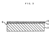
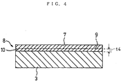
- Figs. 1 to 4 are views illustrating steps of the method of producing such a single crystal SiC composite material for producing a semiconductor device of the invention.
- a single crystal SiC film 2 in which the thickness t2 is about 1 ⁇ m is formed by the heteroepitaxial growth method on a single crystal Si substrate 1 in which the thickness t1 is about 0.5 cm.
- the residual Si substrate 1 in the stacked member 5 is dissolved by using a mixed acid of hydrofluoric acid (HF) and nitric acid (HNO 3 ) to be completely removed away, to obtain a composite member 6 in which, as shown in Fig. 3, only the single crystal SiC film 2 is bonded onto the surface 3a of the polycrystalline plate 3 via the SiO 2 layer 4.
- HF hydrofluoric acid
- HNO 3 nitric acid
- the solid phase growth is performed in which the thermally decomposed Si atoms, and Si and C atoms that sublime from the surface of the polycrystalline plate 3 are rapidly diffused and moved toward the single crystal SiC film 2 which is maintained at a lower temperature, and the portion extending from the bonding interface 9 of the polycrystalline plate 3 by a thickness t4 of about 200 ⁇ m is rearranged in accordance with the single crystal orientation of the single crystal SiC film 2.
- the single crystal SiC composite material 8 in which a thick single crystal SiC portion 10 of a high quality is integrally grown on the polycrystalline plate 3 can be obtained.
Landscapes
- Chemical & Material Sciences (AREA)
- Engineering & Computer Science (AREA)
- Crystallography & Structural Chemistry (AREA)
- Materials Engineering (AREA)
- Metallurgy (AREA)
- Organic Chemistry (AREA)
- Inorganic Chemistry (AREA)
- Chemical Kinetics & Catalysis (AREA)
- General Chemical & Material Sciences (AREA)
- Crystals, And After-Treatments Of Crystals (AREA)
- Recrystallisation Techniques (AREA)
- Physical Deposition Of Substances That Are Components Of Semiconductor Devices (AREA)
Abstract
Description
Claims (12)
- A single crystal SiC composite material which is used for producing a semiconductor device, whereina single crystal SiC film is stacked and bonded via a film-like SiO2 layer onto a surface of a polycrystalline plate consisting of Si and C atoms in a closely contacted manner, andsingle crystal SiC is grown on said polycrystalline plate by a heat treatment conducted on the stacked composite member.
- A single crystal SiC composite material for producing a semiconductor device according to claim 1, wherein said composite member is produced by stacking a single crystal SiC film that is produced on an Si substrate by a heteroepitaxial growth method, via said SiO2 layer onto the surface of said polycrystalline plate in a closely contacted manner, bonding said single crystal SiC film to said polycrystalline plate by a heat treatment on said composite material, and removing away said Si substrate under the bonded state by at least one of hydrofluoric acid and nitric acid.
- A single crystal SiC composite material for producing a semiconductor device according to claim 1, wherein said polycrystalline plate is an SiC polycrystalline plate which is produced into a plate-like shape by a thermal chemical vapor deposition method, or an SiC sintered member.
- A single crystal SiC composite material for producing a semiconductor device according to claim 2, wherein said polycrystalline plate is an SiC polycrystalline plate which is produced into a plate-like shape by a thermal chemical vapor deposition method, or an SiC sintered member.
- A method of producing a single crystal SiC composite material which is used for producing a semiconductor device, comprising the steps of:stacking and bonding a single crystal SiC film via a film-like SiO2 layer onto a surface of a polycrystalline plate consisting of Si and C atoms in a closely contacted manner; andheat-treating said stacked composite member, thereby growing single crystal SiC in which crystal is transformed in the same orientation as single crystal of said single crystal SiC film, integrally on said polycrystalline plate.
- A method of producing a single crystal SiC composite material for producing a semiconductor device according to claim 5, wherein said composite member is produced by stacking a single crystal SiC film that is produced on an Si substrate by a heteroepitaxial growth method, via said SiO2 layer onto the surface of said polycrystalline plate in a closely contacted manner, bonding said single crystal SiC film to said polycrystalline plate by a heat treatment on said composite material at a temperature of 1,100 to 1,500°C, and, after the bonding, removing away said Si substrate by at least one of hydrofluoric acid and nitric acid.
- A method of producing a single crystal SiC composite material for producing a semiconductor device according to claim 5, wherein said polycrystalline plate is an SiC polycrystalline plate which is produced into a plate-like shape by a thermal chemical vapor deposition method, or an SiC sintered member.
- A method of producing a single crystal SiC composite material for producing a semiconductor device according to claim 6, wherein said polycrystalline plate is an SiC polycrystalline plate which is produced into a plate-like shape by a thermal chemical vapor deposition method, or an SiC sintered member.
- A method of producing a single crystal SiC composite material for producing a semiconductor device according to claim 5, wherein said SiO2 layer is formed into a film-like shape by application of SiO2 powder or a silicon compound, or thermal oxidation of said single crystal SiC film and/or the surface of said polycrystalline plate.
- A method of producing a single crystal SiC composite material for producing a semiconductor device according to claim 6, wherein said SiO2 layer is formed into a film-like shape by application of SiO2 powder or a silicon compound, or thermal oxidation of said single crystal SiC film and/or the surface of said polycrystalline plate.
- A method of producing a single crystal SiC composite material for producing a semiconductor device according to claim 5, wherein a temperature of the heat treatment on said composite member is set to a range of 1,850 to 2,000°C.
- A method of producing a single crystal SiC composite material for producing a semiconductor device according to claim 6, wherein a temperature of the heat treatment on said composite member is set to a range of 1,850 to 2,000°C.
Applications Claiming Priority (2)
| Application Number | Priority Date | Filing Date | Title |
|---|---|---|---|
| JP11236968A JP3087070B1 (en) | 1999-08-24 | 1999-08-24 | Single crystal SiC composite material for semiconductor device production and method for producing the same |
| JP23696899 | 1999-08-24 |
Publications (3)
| Publication Number | Publication Date |
|---|---|
| EP1079007A2 true EP1079007A2 (en) | 2001-02-28 |
| EP1079007A3 EP1079007A3 (en) | 2003-11-05 |
| EP1079007B1 EP1079007B1 (en) | 2007-10-17 |
Family
ID=17008443
Family Applications (1)
| Application Number | Title | Priority Date | Filing Date |
|---|---|---|---|
| EP00117180A Expired - Lifetime EP1079007B1 (en) | 1999-08-24 | 2000-08-10 | Single crystal SiC composite material for producing a semiconductor device and a method of producing the same |
Country Status (5)
| Country | Link |
|---|---|
| US (1) | US6524385B1 (en) |
| EP (1) | EP1079007B1 (en) |
| JP (1) | JP3087070B1 (en) |
| DE (1) | DE60036761T2 (en) |
| TW (1) | TW539782B (en) |
Families Citing this family (4)
| Publication number | Priority date | Publication date | Assignee | Title |
|---|---|---|---|---|
| WO2006090432A1 (en) * | 2005-02-22 | 2006-08-31 | Neomax Co., Ltd. | PROCESS FOR PRODUCING SiC SINGLE-CRYSTAL SUBSTRATE |
| JP5672786B2 (en) * | 2010-06-15 | 2015-02-18 | 株式会社デンソー | Method for manufacturing silicon carbide semiconductor substrate and silicon carbide semiconductor device using the substrate |
| JP6572694B2 (en) * | 2015-09-11 | 2019-09-11 | 信越化学工業株式会社 | Method for manufacturing SiC composite substrate and method for manufacturing semiconductor substrate |
| JP6515757B2 (en) * | 2015-09-15 | 2019-05-22 | 信越化学工業株式会社 | Method of manufacturing SiC composite substrate |
Family Cites Families (8)
| Publication number | Priority date | Publication date | Assignee | Title |
|---|---|---|---|---|
| EP1531491A2 (en) * | 1996-04-18 | 2005-05-18 | Matsushita Electric Industrial Co., Ltd. | SiC device and method for manufacturing the same |
| JP3296998B2 (en) * | 1997-05-23 | 2002-07-02 | 日本ピラー工業株式会社 | Single crystal SiC and method for producing the same |
| US6153166A (en) * | 1997-06-27 | 2000-11-28 | Nippon Pillar Packing Co., Ltd. | Single crystal SIC and a method of producing the same |
| JP3043675B2 (en) * | 1997-09-10 | 2000-05-22 | 日本ピラー工業株式会社 | Single crystal SiC and method for producing the same |
| JP3043690B2 (en) * | 1997-11-17 | 2000-05-22 | 日本ピラー工業株式会社 | Single crystal SiC and method for producing the same |
| JP3043689B2 (en) * | 1997-11-17 | 2000-05-22 | 日本ピラー工業株式会社 | Single crystal SiC and method for producing the same |
| JP2884085B1 (en) * | 1998-04-13 | 1999-04-19 | 日本ピラー工業株式会社 | Single crystal SiC and method for producing the same |
| EP1130137B1 (en) * | 1999-07-30 | 2006-03-08 | Nissin Electric Co., Ltd. | Material for raising single crystal sic and method of preparing single crystal sic |
-
1999
- 1999-08-24 JP JP11236968A patent/JP3087070B1/en not_active Expired - Fee Related
-
2000
- 2000-06-16 TW TW089111876A patent/TW539782B/en active
- 2000-08-08 US US09/634,599 patent/US6524385B1/en not_active Expired - Fee Related
- 2000-08-10 EP EP00117180A patent/EP1079007B1/en not_active Expired - Lifetime
- 2000-08-10 DE DE60036761T patent/DE60036761T2/en not_active Expired - Lifetime
Also Published As
| Publication number | Publication date |
|---|---|
| DE60036761D1 (en) | 2007-11-29 |
| DE60036761T2 (en) | 2008-07-17 |
| EP1079007A3 (en) | 2003-11-05 |
| EP1079007B1 (en) | 2007-10-17 |
| JP2001064096A (en) | 2001-03-13 |
| JP3087070B1 (en) | 2000-09-11 |
| TW539782B (en) | 2003-07-01 |
| US6524385B1 (en) | 2003-02-25 |
Similar Documents
| Publication | Publication Date | Title |
|---|---|---|
| EP2314737B1 (en) | Method of producing a high quality single crystal of silicon carbide in a seeded growth system | |
| US6153166A (en) | Single crystal SIC and a method of producing the same | |
| JP5498163B2 (en) | Multilayer semiconductor wafer, method of manufacturing the same, and element | |
| US6083812A (en) | Heteroepitaxy by large surface steps | |
| US6326667B1 (en) | Semiconductor devices and methods for producing semiconductor devices | |
| JP6508050B2 (en) | Method of manufacturing silicon carbide ingot, method of manufacturing silicon carbide substrate, and method of manufacturing semiconductor device | |
| TW201212286A (en) | Method for manufacturing nitride semiconductor crystal layer | |
| EP0964081B1 (en) | Method of producing a single crystal of SiC | |
| EP0921214B1 (en) | Single crystal silicon carbide and process for preparing the same | |
| KR20230009363A (en) | Base substrate for crystallization of group III-V compound and method for manufacturing the same | |
| EP1079007B1 (en) | Single crystal SiC composite material for producing a semiconductor device and a method of producing the same | |
| EP1424410A1 (en) | Semiconductor crystal producing method | |
| EP1130137B1 (en) | Material for raising single crystal sic and method of preparing single crystal sic | |
| KR100288473B1 (en) | SINGLE CRYSTAL SiC AND PROCESS FOR PREPARING THE SAME | |
| JP3487254B2 (en) | Single crystal SiC and method for producing the same | |
| US7112243B2 (en) | Method for producing Group III nitride compound semiconductor | |
| JP3551106B2 (en) | Method for producing single crystal SiC | |
| JP3087030B2 (en) | SiC composite, method for producing the same, and single crystal SiC | |
| JP2917149B1 (en) | Single crystal SiC and method for producing the same | |
| JP2002261011A (en) | Multilayer substrate for device | |
| EP2172967A1 (en) | Method for manufacturing silicon carbide | |
| CN1434153A (en) | Method for preparing expitaxial hetero crystal and film material on yield substrate | |
| JP3043687B2 (en) | Single crystal SiC and method for producing the same |
Legal Events
| Date | Code | Title | Description |
|---|---|---|---|
| PUAI | Public reference made under article 153(3) epc to a published international application that has entered the european phase |
Free format text: ORIGINAL CODE: 0009012 |
|
| 17P | Request for examination filed |
Effective date: 20000908 |
|
| AK | Designated contracting states |
Kind code of ref document: A2 Designated state(s): AT BE CH CY DE DK ES FI FR GB GR IE IT LI LU MC NL PT SE |
|
| AX | Request for extension of the european patent |
Free format text: AL;LT;LV;MK;RO;SI |
|
| RAP1 | Party data changed (applicant data changed or rights of an application transferred) |
Owner name: NISSIN ELECTRIC CO., LTD. |
|
| PUAL | Search report despatched |
Free format text: ORIGINAL CODE: 0009013 |
|
| AK | Designated contracting states |
Kind code of ref document: A3 Designated state(s): AT BE CH CY DE DK ES FI FR GB GR IE IT LI LU MC NL PT SE |
|
| AX | Request for extension of the european patent |
Extension state: AL LT LV MK RO SI |
|
| RIC1 | Information provided on ipc code assigned before grant |
Ipc: 7C 30B 23/02 B Ipc: 7C 30B 25/02 A Ipc: 7C 30B 29/36 B Ipc: 7C 30B 33/06 B |
|
| 17Q | First examination report despatched |
Effective date: 20040608 |
|
| AKX | Designation fees paid |
Designated state(s): DE FR GB |
|
| GRAP | Despatch of communication of intention to grant a patent |
Free format text: ORIGINAL CODE: EPIDOSNIGR1 |
|
| GRAC | Information related to communication of intention to grant a patent modified |
Free format text: ORIGINAL CODE: EPIDOSCIGR1 |
|
| GRAJ | Information related to disapproval of communication of intention to grant by the applicant or resumption of examination proceedings by the epo deleted |
Free format text: ORIGINAL CODE: EPIDOSDIGR1 |
|
| GRAP | Despatch of communication of intention to grant a patent |
Free format text: ORIGINAL CODE: EPIDOSNIGR1 |
|
| GRAS | Grant fee paid |
Free format text: ORIGINAL CODE: EPIDOSNIGR3 |
|
| GRAA | (expected) grant |
Free format text: ORIGINAL CODE: 0009210 |
|
| AK | Designated contracting states |
Kind code of ref document: B1 Designated state(s): DE FR GB |
|
| REG | Reference to a national code |
Ref country code: GB Ref legal event code: FG4D |
|
| REF | Corresponds to: |
Ref document number: 60036761 Country of ref document: DE Date of ref document: 20071129 Kind code of ref document: P |
|
| ET | Fr: translation filed | ||
| PLBE | No opposition filed within time limit |
Free format text: ORIGINAL CODE: 0009261 |
|
| STAA | Information on the status of an ep patent application or granted ep patent |
Free format text: STATUS: NO OPPOSITION FILED WITHIN TIME LIMIT |
|
| 26N | No opposition filed |
Effective date: 20080718 |
|
| GBPC | Gb: european patent ceased through non-payment of renewal fee |
Effective date: 20080810 |
|
| REG | Reference to a national code |
Ref country code: FR Ref legal event code: ST Effective date: 20090430 |
|
| PG25 | Lapsed in a contracting state [announced via postgrant information from national office to epo] |
Ref country code: FR Free format text: LAPSE BECAUSE OF NON-PAYMENT OF DUE FEES Effective date: 20080901 |
|
| PG25 | Lapsed in a contracting state [announced via postgrant information from national office to epo] |
Ref country code: GB Free format text: LAPSE BECAUSE OF NON-PAYMENT OF DUE FEES Effective date: 20080810 |
|
| PGFP | Annual fee paid to national office [announced via postgrant information from national office to epo] |
Ref country code: DE Payment date: 20100823 Year of fee payment: 11 |
|
| REG | Reference to a national code |
Ref country code: DE Ref legal event code: R119 Ref document number: 60036761 Country of ref document: DE Effective date: 20120301 |
|
| PG25 | Lapsed in a contracting state [announced via postgrant information from national office to epo] |
Ref country code: DE Free format text: LAPSE BECAUSE OF NON-PAYMENT OF DUE FEES Effective date: 20120301 |