BACKGROUND OF THE INVENTION
-
The present invention relates to a dielectric film having
an ABO3 perovskite structure with a high dielectric constant
suitably used as a dielectric film for sandwiching upper and lower
conducting electrodes in a thin film capacitor and a method of
fabricating the dielectric film.
-
Recently, electronic equipment is desired to have small size
and thickness. Electronic equipment includes a circuit substrate
or the like mounting electronic components (elements) such as an
IC and a capacitor, and therefore, an electronic component and
a circuit substrate used in electronic equipment are also required
to have small area and thickness. Among such electronic components
(elements), a capacitor in particular occupies a large area, and
hence, reduction in its area can lead to a great effect in reducing
the area and the thickness of the electronic component.
-
On the other hand, a memory utilizing charge and polarization
of a capacitor is remarkably widely used these days, and various
structures have been proposed for a capacitor. For example, in
order to realize a compact and thin capacitor, not only a
semiconductor substrate is used but also a compact, light and
inexpensive substrate, such as glass, ceramics, a metallic foil
and a flexible organic polymer film, is used, so as to provide
a compact and light thin film capacitor having a laminated structure
including electrode thin films and a highly dielectric thin film.
-
In particular, a dielectric film having a perovskite
structure whose stoichiometric composition is represented by ABO3
(wherein A and B are metal atoms) has a large dielectric constant
and is a significant material in reducing the area and the size
of the electronic component. Also, a dielectric film having the
perovskite structure has, depending upon its orientation and kind,
a hysteresis characteristic that predetermined polarization
remains after removal of voltage application, and hence, such a
dielectric film can function as a ferroelectric film. Since SrTiO3
(namely, so-called STO), that is, one of dielectrics having the
perovskite structure, has a comparatively large dielectric
constant, its use in a thin film capacitor for a non-contact IC
card is now increasing.
-
A dielectric film having the perovskite structure is
generally formed by CVD such as so-called MOCVD utilizing a reaction
of an organic metal, and is sometimes formed by sputtering,
deposition or the like for the purpose of improving through-put
and reducing fabrication cost.
-
Although a dielectric film having the perovskite structure
has the aforementioned good characteristics but also has unsolved
problems as follows:
-
First, although a dielectric film having the perovskite
structure has a large dielectric constant and a ferroelectric
property, it is known that these dielectric characteristics depend
upon the crystallinity of the dielectric film. It is known, for
example, that the dielectric constant and residual polarization
can be lowered when the dielectric film is poor at the crystallinity
and the orientation. When the sputtering is employed for the
purpose of fabricating an inexpensive thin film capacitor, the
composition of the dielectric film is often shifted from the
stoichiometric composition, and in such a case, the crystallinity
is degraded. As a result, the desired dielectric characteristics
cannot be always attained.
-
Also, when the thickness of the dielectric film is reduced
so as to reduce the thickness of the element and increase the
capacitance, a leakage current tends to unavoidably increase. In
particular, when a dielectric film having the ABO3 perovskite
structure includes a large number of crystal defects, much leakage
occurs. Such crystal defects include loss of an oxygen atom (O)
(oxygen loss) in a crystal lattice of the perovskite structure
represented by ABO3 and shift of the existing ratio between the
metal atoms A and B from 1:1. These crystal defects can result
in various problems, and for example, breakdown can easily occur
in the dielectric film, data stored in the dielectric film serving
as a memory can be easily volatized, or when the dielectric film
is used as a ferroelectric film, sufficient polarization cannot
be attained by applying a voltage.
-
These problems are particularly conspicuous when the
dielectric film is formed by sputtering or deposition carried out
at a low temperature. In other words, when the dielectric film
is formed at a high deposition rate, in particular, at a low
temperature by the sputtering or deposition so as to improve the
through-put for the purpose of lowering the fabrication cost, a
phenomenon such as degradation in the crystallinity and occurrence
of crystal defects can be easily caused. In fabrication of a thin
film capacitor formed on a flexible organic film with low heat
resistance as in application to an IC card or the like, the dielectric
film is unavoidably formed at a low temperature. Accordingly,
it is difficult to fabricate, at low cost, a thin film capacitor
including a dielectric film with the ABO3 perovskite structure,
such as an STO film, formed on a substrate with low heat resistance.
-
An object of the invention is providing a dielectric film
having the ABO3 perovskite structure that can be fabricated at
low cost with keeping good dielectric characteristics such as a
leakage characteristic, and a method of fabricating the dielectric
film.
SUMMARY OF THE INVENTION
-
The dielectric film of this invention has a perovskite
structure with a stoichiometric composition represented by ABO3,
including a group II element A, a group IV element B and oxygen
O, and the perovskite structure includes nitrogen.
-
Accordingly, owing to nitrogen included in the perovskite
structure, leakage caused in applying a voltage to the dielectric
film upward or downward can be reduced. Also, the dielectric film
can attain improved crystallinity and minuteness. Therefore,
other characteristics, such as a dielectric constant, residual
polarization in applying a voltage to the dielectric film upward
or downward, and dielectric loss, can be improved.
-
In the dielectric film, the nitrogen is bonded to at least
one of the element A and the element B. Therefore, an effect to
suppress electron tunneling can be definitely attained.
-
In the dielectric film, the nitrogen is included in the
perovskite structure in a concentration of 5 at % or less. Therefore,
a problem caused by excessive nitrogen can be avoided.
-
In the dielectric film, the element A is at least one material
selected from the group consisting of Sr, Ba, Bi, La and Pb and
the element B is at least one material selected from the group
consisting of Ti, Ca, Nb, and Zr. Therefore, the invention is
applicable to a widely used dielectric film having a perovskite
structure.
-
The dielectric film of this invention may function as a
capacitor dielectric film of a capacitor disposed on a substrate
made from an organic material, namely, a capacitor formed on a
so-called flexible substrate. Thus, a capacitor dielectric film
made from a dielectric film with a high dielectric constant can
be realized at low cost. In other words, a high quality and highly
reliable thin film capacitor with large capacitance, small loss,
a small leakage current and a high breakdown voltage can be obtained.
-
The first method of this invention of fabricating a
dielectric film having a perovskite structure with a stoichiometric
composition represented by ABO3, including a group II element A,
a group IV element B and oxygen O, comprises a step (a) of supplying
a gas including an element lighter than Ar and a gas including
oxygen into a chamber; and a step (b) of depositing the dielectric
film having the perovskite structure including the element A, the
element B and oxygen on an object surface by drawing atoms of the
element A and atoms of the element B from a metal material into
a space within the chamber.
-
In this method, the existing ratio between the atoms of the
element A and the atoms of the element B drawn into the space within
the chamber can be adjusted, even at a low temperature, so as to
attain a condition for forming a dielectric film having a
composition close to the stoichiometric composition of the ABO3
perovskite structure. Accordingly, a dielectric film good at
dielectric characteristics can be formed on a substrate with low
heat resistance.
-
In the first method, an Ar gas maybe supplied into the chamber
in addition to the gas including an element lighter than Ar in
the step (a). In this manner, the existing ratio between the atoms
of the element A and the atoms of the element B drawn into the
space within the chamber can be more easily adjusted to fall within
an appropriate range also by utilizing comparatively heavy Ar
atoms.
-
It is experimentally confirmed that a mixed gas including
an Ar gas, an oxygen gas and a nitrogen-containing gas is preferably
supplied into the chamber in the step (a).
-
When the atoms of the element A and the element B are drawn
into the space within the chamber by sputtering from the metal
material in the step (b), the deposition rate for the dielectric
film can be increased, which can make the method suitable to
mass-production.
-
When the dielectric film is deposited at a rate of 10 nm/min.
or more in the step (b), the productivity is improved, resulting
in forming the dielectric film at low cost.
-
When the object surface used in the step (b) is a top surface
of a metal electrode disposed on a substrate made from an organic
material, a dielectric film with good characteristics can be formed
on a flexible substrate or the like at a low temperature. As a
result, an inexpensive capacitor can be fabricated by using the
dielectric film of this invention. In other words, the method
is applicable to fabrication of a high quality and highly reliable
thin film capacitor with large capacitance, small loss, a small
leakage current and a high breakdown voltage.
-
The second method of this invention of fabricating a
dielectric film having a perovskite structure with a stoichiometric
composition represented by ABO3, including a group II element A,
a group IV element B and oxygen O, comprises a step (a) of supplying
at least two kinds of sputtering gases having different weights
and an oxygen-containing gas into a chamber; a step (b) of setting
the two kinds of sputtering gases and the oxygen-containing gas
to a plasma state; and a step (c) of depositing the dielectric
film having the perovskite structure including the element A, the
element B and oxygen on an object surface by striking a target
material with atoms of the two kinds of sputtering gases in a plasma
state so as to draw atoms of the element A and atoms of the element
B into a space within the chamber.
-
In this method, the elements A and B are sputtered by the
at least two kinds of gases having different weights, and hence,
a ratio in the sputtered amount between the elements A and B can
be varied by varying the flow ratio between the two kinds of gases.
Specifically, by adjusting the flow ratio of the at least two kinds
of gases, the existing ratios between the elements A and B can
be adjusted to be optimal for attaining the stoichiometric
composition.
-
In the second method, the two kinds of sputtering gases are
preferably inert gases.
BRIEF DESCRIPTION OF THE DRAWINGS
-
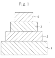
- Figure 1 is a cross-sectional view of a thin film capacitor
according to Embodiment 1 of the invention;
- Figures 2(a), 2(b), 2(c), 2(d) and 2(e) are cross-sectional
views for showing procedures in fabrication of the thin film
capacitor of Embodiment 1;
- Figures 3(a) and 3(b) are diagrams of images obtained through
analysis, with a scanning electron microscope (SEM), of surfaces
of SrTiO3 films of a comparative example and Embodiment 1;
- Figures 4(a) and 4(b) are diagrams of profiles obtained
through analysis with SIMS of change in components along a depth
direction in the SrTiO3 films of the comparative example and
Embodiment 1;
- Figure 5 is a diagram for showing a result of analysis with
XPS of a bond state of nitrogen in the SrTiO3 film of Embodiment
1 formed by using an Ar/O2/N2 gas as a film forming gas;
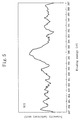
- Figure 6 is a diagram of an emission spectrum obtained as
a result of analysis with CL of the SrTiO3 films of the comparative
example and Embodiment 1;
- Figures 7(a) and 7(b) are diagrams for showing estimated
models of crystal structures of SrTiO3 films formed by respectively
using an Ar/O2 gas and an Ar/O2/N2 gas;
- Figure 8 is a partial band chart for explaining mechanism
of leakage in a thin film capacitor including a dielectric film
with the ABO3 perovskite structure;
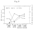
- Figure 9 is a diagram for showing data obtained through
analysis with OES of plasma atmospheres for forming the SrTiO3
films of the comparative example and Embodiment 1 with conditions
varied;
- Figures 10(a) and 10(b) are SEM photographs of the surfaces
of the SrTiO3 films formed by respectively using an Ar/O2 gas and
an Ar/O2/N2 gas as the film forming gas;
- Figure 11 is a diagram of a Ti/Sr emission intensity ratio
in using a He gas, a Ne gas, an Ar gas or a Xe gas together with
an O2 gas as the film forming gas; and
- Figures 12(a), 12(b) and 12(c) are SEM photographs of SrTiO3
films formed by respectively using a He gas, an Ar gas and a Xe
gas as a rare gas included in the film forming gas.
-
DETAILED DESCRIPTION OF THE INVENTION
EMBODIMENT 1
-
Figure 1 is a sectional view for showing the structure of
a thin film capacitor according to Embodiment 1. As is shown in
Figure 1, the thin film capacitor of this embodiment includes a
bottom electrode 2 of a Pt/Ti laminated film disposed on a substrate
1 of a boro-silicated glass, a capacitor dielectric film 3 of a
SrTiO3 film disposed on the bottom electrode 2, and a top electrode
4 of a Pt film disposed on the capacitor dielectric film 3. In
other words, the thin film capacitor has a structure in which the
capacitor dielectric film 3 is sandwiched between the bottom
electrode 2 and the top electrode 4.
-
Next, a method of fabricating the thin film capacitor of
this embodiment will be described. Figures 2(a) through 2(e) are
sectional views for showing procedures in the fabrication of the
thin film capacitor of this embodiment.
-
First, in the procedure shown in Figure 2(a), a substrate
1 of a boro-silicated glass with a thickness of 0.5 mm is prepared,
and a Pt/Ti film 10 to be formed into a bottom electrode is formed
on the substrate 1 by DC sputtering. The DC sputtering is carried
out, for example, within a high vacuum chamber evacuated to a level
of 10-6 Torr (0.0013Pa) in an atmosphere of Ar at DC power of 200
W, at a film forming pressure of 8 x 10⁻³ Torr (1.1 Pa) and at
a temperature of the substrate of 25°C. In the Pt/Ti film 10,
a Pt film has a thickness of 100 nm and a Ti film has a thickness
of 10 nm. Furthermore, these films are both deposited at a
deposition rate of approximately 10 nm/min.
-
Next, in the procedure shown in Figure 2(b), the Pt/Ti film
is patterned by using a metal mask, thereby forming a bottom
electrode 2 on the substrate 1. The bottom electrode 2 has a size
of approximately 5 x 5 mm.
-
Then, in the procedure shown in Figure 2(c), a SrTiO3 film
11, that is, a dielectric film to be formed into a capacitor
dielectric film, is formed on the substrate by RF magnetron
sputtering. In forming the SrTiO3 film 11, a mixture of an Ar
gas, an O2 gas and a N2 gas is used as a film forming gas. Specifically,
Ar ions generated by plasma are allowed to strike Sr and Ti targets,
so that Sr atoms and Ti atoms can be sputtered owing to a momentum
exchange function. As a result, O atoms included in the atmosphere
and the sputtered Sr and Ti atoms are deposited on the substrate,
thereby forming the SrTiO3 film. As the conditions for the
sputtering, the pressure within the chamber is reduced to high
vacuum at a level of 10-6 Torr (0.13 mPa), the film forming pressure
is set to 8 x 10⁻³ Torr (1.1 Pa), the RF power is set to 200 W
and the temperature of the substrate is set to 200°C.
-
In this embodiment, the SrTiO3 film is formed by the
sputtering conducted within a film forming gas including Ar, O2
and N2 in a mixing ratio of 2:1:0.5. The SrTiO3 film 11 has a
thickness of approximately 300 nm, and the deposition rate is
approximately 3.0 nm/min.
-
Next, in the procedure shown in Figure 2(d), the SrTiO3 film
11 is patterned, thereby forming a capacitor dielectric film 3
on the bottom electrode 2. The capacitor dielectric film 3 has
a size of approximately 4 x 4 mm.
-
Then, in the procedure shown in Figure 2(e), a Pt film is
deposited on the substrate by DC magnetron sputtering, and the
Pt film is patterned into atop electrode 4 disposed on the capacitor
dielectric film 3. The Pt film to be formed into the top electrode
4 is deposited under the same conditions as in depositing the Pt
film included in the bottom electrode 2. The top electrode 4 has
a plane size of approximately 3 x 3 mm. Accordingly, a portion
of the capacitor dielectric film 3 sandwiched between the bottom
electrode 2 and the top electrode 4 has a size of approximately
3 x 3 mm.
-
In the fabrication method of this embodiment, a N2 gas is
used in addition to an Ar/O2 gas as the film forming gas. Therefore,
as compared with the case where an Ar/O2 gas alone is used as the
film forming gas, the SrTiO3 film can attain a large dielectric
constant and less leakage. Since such a SrTiO3 film is used, the
thin film capacitor can attain good characteristics as described
in detail below.
-Comparison in characteristics between embodiment and comparative
example -
-
In order to compare the SrTiO3 film formed as described above
and the thin film capacitor using the SrTiO3 film with a conventional
product, a SrTiO3 film is formed as a comparative example by using
a mixed gas including Ar and O2 in a ratio of 2:1 as the film forming
gas in the procedure shown in Figure 2(c). This SrTiO3 film has
a thickness of approximately 300 nm, and the deposition rate is
approximately 3.5 nm/min. Now, results of various evaluations
will be described for comparing the SrTiO3 films of this embodiment
and the comparative example in their structures and
characteristics.
-
Figures 3(a) and 3(b) are diagrams of images obtained through
analysis with a scanning electron microscope (SEM) of the surfaces
of the SrTiO3 films in the laminated films having a
Pt/SrTiO3/Pt/Ti/glass structure formed in the comparative example
and this embodiment. Figure 3(a) reveals that the SrTiO3 film
formed by using the Ar/O2 gas as the film forming gas has large
irregularities on the surface and rough grain boundaries. In
contrast, Figure 3(b) reveals that the SrTiO3 film formed by using
the Ar/O2/N2 gas as the film forming gas has small irregularities
on the surface and minute grain boundaries.
-
Figures 4(a) and 4(b) are diagrams of profiles obtained
through analysis with secondary ion mass spectrometry (SIMS) of
change in composition along the depth direction in the laminated
films having the Pt/SrTiO3/Pt/Ti/glass structure formed in the
comparative example and this embodiment. Figure 4(a) reveals that
the SrTiO3 film formed by using the Ar/O2 gas as the film forming
gas has a nitrogen concentration of approximately 1016/cm3. In
contrast, Figure 4(b) reveals that the SrTiO3 film formed by using
the Ar/O2/N2 gas as the film forming gas includes more nitrogen
than the SrTiO3 film formed by using the Ar/O2 gas. In addition,
nitrogen is uniformly present in this SrTiO3 film. The nitrogen
concentration in this SrTiO3 film calculated on the basis of the
depth profile of SIMS is approximately 3 at%.
-
Figure 5 is a diagram for showing the result of analysis
with X-ray photoelectron spectroscopy (XPS) of a bond state of
nitrogen in the SrTiO3 film of this embodiment formed by using
the Ar/O2/N2 gas as the film forming gas. In obtaining data shown
in this drawing, nitrogen is identified by using the N1S spectrum.
In general, nitrogen as a simple substance has a binding energy
of 399 through 400 eV. According to the data of Figure 5, however,
nitrogen included in the SrTiO3 film of this embodiment formed
by using the Ar/O2/N2 gas is in a bond state with a lower energy
of approximately 396 eV, which probably means that the nitrogen
is bonded to any metal. Specifically, the nitrogen seems to present
within the SrTiO3 film in a state bonded to Sr or Ti. In the
(conventional) SrTiO3 film of the comparative example formed by
using the Ar/O2 gas as the film forming gas, the concentration
of the nitrogen element is approximately 1016/cm3, and hence, the
content of nitrogen is too small to observe the N1S spectrum with
XPS.
-
Figure 6 shows emission spectra obtained as a result of
analysis with a cathode luminescence (CL) of the SrTiO3 films
included in the laminated films having the Pt/SrTiO3/Pt/Ti/glass
structure of the comparative example and this embodiment. As shown
in Figure 6, a CL spectrum in the vicinity of a wavelength of 530
nm corresponds to an emission spectrum related to oxygen loss.
In the SrTiO3 film of this embodiment formed by using the Ar/O2/N2
gas as the film forming gas, the intensity of the CL spectrum is
remarkably lower than in the SrTiO3 film of the comparative example
formed by using the Ar/O2 gas as the film forming gas. In other
words, it seems that the SrTiO3 film of this embodiment formed
by using the Ar/O2/N2 gas includes nitrogen and the nitrogen is
bonded to the metal, so as to compensate the harmful effect of
the oxygen loss in the SrTiO3 film.
-
Figures 7(a) and 7(b) are diagrams for showing estimated
models of the crystal structures of the SrTiO3 films formed by
using the Ar/O2 gas and the Ar/O2/N2 gas, respectively. As is shown
in Figure 7(a), in a SrTiO3 lattice of the comparative example
formed by using the Ar/O2 gas, a hole (shown with a broken line)
is formed due to the oxygen loss. In contrast, in a SrTiO3 lattice
of this embodiment formed by the Ar/O2/N2 gas, it seems that nitrogen
is substituted for a hole as is shown in Figure 7(b), or that a
nitrogen atom is bonded to a metal atom through any bonding in
any position within the lattice. Since the nitrogen atom is linked
with a bond of a metal atom unlinked due to the hole, the harmful
effect of the oxygen loss can be compensated so as to reduce leakage
as described in detail below.
-
Table 1 shows the results of evaluations of various
characteristics of thin film capacitors including the SrTiO
3 films
formed by using the Ar/O
2 gas and the Ar/O
2/N
2 gas, respectively.
A value corresponding to each characteristic listed in this table
is obtained at a measurement frequency of 1 kHz, and a leakage
current listed in the table is obtained by applying a voltage of
+5 V to the top electrode with the bottom electrode grounded.
| Dependence of capacitor characteristics on film
forming gas |
| Film forming gas for SrTiO3 film | Ar/O2 | Ar/O2/N2 |
| ε r | 70 | 80 |
| tan δ(%) | 0.7 | 0.4 |
| I(mA/cm2) | 2.1 x 10⁻⁶ | 2.6 x 10⁻⁷ |
-
As listed in Table 1, the SrTiO3 film of the comparative
example formed by using the Ar/O2 gas has a dielectric constant
of 70, dielectric loss tangent of 0.7% and a current density of
2.1 x 10⁻⁶ mA/cm2. In contrast, the SrTiO3 film of this embodiment
formed by using the Ar/O2/N2 gas has a dielectric constant of 80.
dielectric loss tangent of 0.4% and a current density of 2.6 x
10-7 mA/cm2. In this manner, the SrTiO3 film of this embodiment
has a larger dielectric constant, smaller dielectric loss tangent
and a smaller leakage current than the conventional SrTiO3 film
(of the comparative example). These differences in the
characteristic values such as the dielectric loss tangent and the
current density between this embodiment and the comparative example
are probably derived from the differences in the fine structure
and the crystallinity between the SrTiO3 films observed with SEM,
SIMS, XPS and CL.
- Mechanism of occurrence of leakage and effect attained by reducing
leakage -
-
Figure
8 is a partial band chart for explaining the mechanism
of leakage occurring in a thin film capacitor including a dielectric
film with the ABO
3 perovskite structure such as a SrTiO
3 (STO)
film. As is shown in Figure
8, the procedure of occurrence of
a leakage current is roughly divided into tunneling through a
potential barrier and jump over a potential barrier. The tunneling
through a potential barrier is classified into:
- 1 ○ tunneling from a valence band to a conduction band;
- 2 ○ tunneling from an impurity level to a conduction band;
- 3 ○ tunneling from a bottom electrode (electrode with lower
potential) to a conduction band; and
- 4 ○ tunneling from a valence band to a top electrode (electrode
with higher potential).
On the other hand, the jump over a potential barrier is
classified into:
- 5 ○ jump from a top electrode to a conduction band owing to
the Schottky effect; and
- 6 ○ jump from an impurity level to a conduction band owing
to the Poole-Frenkel effect.
-
-
It seems that 1 ○ the tunneling from a valence band to a
conduction band is caused mainly by electrons flowing through a
grain boundary, and hence, it is necessary to reduce the area of
a grain boundary. The area of a grain boundary can be probably
reduced by forming a dielectric film with the ABO3 perovskite
structure, such as a SrTiO3 film, oriented along one direction
(specifically, along a direction where the film surface accords
with the (111) surface orientation), so as to increase the
minuteness of the dielectric film.
-
2 ○ The tunneling from an impurity level to a conduction band
is caused mainly because oxygen loss formed within a dielectric
film having the ABO3 perovskite structure generates donor levels
and electrons captured by the donor levels tunnel into the
conduction band. Accordingly, the leakage resulting from this
tunneling can be reduced by forming a dielectric film having the
ABO3 perovskite structure including less donor levels derived from
the oxygen loss.
-
3 ○ The tunneling from a bottom electrode to a conduction
band and 4 ○ the tunneling from a valence band to a top electrode
are probably caused by electrons piercing from the electrode to
the conduction band or from the valence band to the electrode through
a space-charge region present on one surface closer to the
dielectric film of a Schottky barrier, which is considered to be
formed in a contact portion between an electrode and a dielectric
film. Accordingly, it is significant to suppress the pierce of
the electrons by increasing the width of the space-charge region.
In order to increase the width of the space-charge region, it is
significant to reduce the carrier concentration in the dielectric
film, namely, to reduce lattice defects causing donor levels in
the dielectric film.
-
5 ○ The jump from a top electrode to a valence band is probably
caused by electrons released beyond the Schottky barrier that is
considered to be formed between an electrode and a dielectric film.
Accordingly, this electron jump can be suppressed by increasing
the height of the Schottky barrier (Φm - x), and the height of
the Schottky barrier can be increased by increasing the work
function Φm of the bottom electrode.
-
6 ○ The jump form an impurity level to a conduction band is
probably caused because oxygen loss and the like formed within
a perovskite dielectric film generate donor levels and electrons
captured by the donor levels jump over a potential difference
between the donor levels and the conduction band. Accordingly,
leakage resulting from this jump can be reduced by forming a
dielectric film including less donor levels derived from the oxygen
loss.
-
As described so far, in order to reduce leakage in a dielectric
film having the ABO3 perovskite structure, reduction of donor levels
derived from the oxygen loss and reduction of defects such as lattice
defects (namely, improvement of crystallinity) are particularly
effective.
-
As is obvious from the aforementioned evaluation results,
the SrTiO3 film formed by the fabrication method of this embodiment
has a high nitrogen concentration, and nitrogen is incorporated
into the crystal lattice to be bonded to Sr or Ti. Since the nitrogen
is thus bonded to Sr or Ti, the donor levels derived from the oxygen
loss are probably reduced. It seems that the leakage is reduced
because the harmful effect of the oxygen loss is thus compensated
by the nitrogen. Furthermore, when nitrogen is incorporated into
the oxygen loss in the SrTiO3 film, the resultant film structure
attains good crystallinity and minuteness. A SrTiO3 film with
good crystallinity having a composition close to the stoichiometric
composition can be formed by adjusting the atmosphere of sputtering
as described below.
-
In this manner, in the dielectric film having the ABO3
(wherein A is a group II element and B is a group IV element)
perovskite structure of this embodiment, the crystallinity is
improved and the donor levels derived from the oxygen loss are
reduced owing to the nitrogen included therein. Since the
dielectric film can thus attain minuteness, the capacitance is
increased, the loss is decreased and a leakage current is reduced.
Furthermore, since heat loss under application of a high frequency
voltage is smaller as a leakage current is smaller, the dielectric
loss tangent (tan δ) is reduced. Accordingly, the fabrication
method of this embodiment provides a high quality and highly
reliable thin film capacitor with a high breakdown voltage.
-
When the nitrogen concentration in the SrTiO3 film exceeds
5 at%, the quality of the film is degraded, resulting in lowering
all the characteristics of the thin film capacitor. Accordingly,
the nitrogen concentration in the SrTiO3 film is preferably 5 at%
or less. Furthermore, the nitrogen concentration in the SrTiO3
film is preferably higher than a nitrogen content attained without
intentionally introducing nitrogen into the dielectric film
(namely, approximately 1016/cm3).
-
The dielectric film is preferably made from at least one
material capable of attaining a high dielectric constant or
spontaneous polarization (ferroelectric property) selected from
the group consisting of SrTiO3, (SrCa)TiO3, (SrBi)TiO3, BaTiO3,
PbTiO3, (PbLa)TiO3, Pb(ZrTi)O3 and a substance including any of
these materials as a solid-solution element.
-
The dielectric film is formed preferably by RF magnetron
sputtering or ECR magnetron sputtering. The deposition rate of
the dielectric film is preferably 10 nm/min. or more from the point
of view of fabrication cost. A rare gas included as an inert gas
in the film forming gas is preferably at least one selected from
the group consisting of He, Ne and Ar.
-Relationship between deposition rate and film characteristic-
-
Figure 9 is a diagram for showing data obtained by analysis
through optical emission spectroscopy (hereinafter referred to
as OES) of plasma atmosphere in forming the SrTiO3 films of this
embodiment and the comparative example with varying the RF power
(high frequency power) and the composition of the film forming
gas. As is shown in Figure 9, the RF power and the film forming
gas employed in forming the SrTiO3 films are set to four conditions:
200 W and an Ar/O2 gas; 1000 W and an Ar/O2 gas; 1000 W and an
Ar/O2/N2 gas (in a flow ratio of 12:5.5:1); and 1000 W and an Ar/O2/N2
gas (in a flow ratio of 12:5.5:5). Also in Figure 9, the ordinate
on the left hand side indicates the OES intensity (in arbitrary
unit) of Sr and Ti, and the ordinate on the right hand side indicates
the Ti/Sr emission intensity ratio, whereas Sr and Ti are different
in the detection sensitivity and hence the emission intensity ratio
does not correspond to the existing ratio between Sr and Ti in
the actual atmosphere. It is empirically known that a SrTiO3 film
having a composition close to the stoichiometric composition can
be formed when the Ti/Sr emission intensity ratio thus detected
is approximately "2". Furthermore, as the composition of the
SrTiO3 film is closer to the stoichiometric composition, the
orientation of the crystal grains is better, which makes easy to
attain the desired dielectric constant and ferroelectric property.
-
As is shown in Figure 9, in using an Ar/O2 gas with the RF
power set to 200 W, the Ti/Sr emission intensity ratio is "2",
which means that a SrTiO3 film with a composition close to the
stoichiometric composition can be formed. However, the
concentrations of Ti and Sr in the atmosphere are low, and hence,
the deposition rate of the film is too low to be suitably employed
in a mass-production process. On the other hand, in using an Ar/O2
gas with the RF power set to 1000 W, although the deposition rates
of Ti and Sr are increased, the Sr concentration is much higher
than the Ti concentration, which makes the composition of the SrTiO3
film largely deviated from the stoichiometric composition.
Therefore, it is difficult to attain the desired ferroelectric
property. In contrast, in using an Ar/O2/N2 gas (in a flow ratio
of 12:5.5:1) with the RF power set to 1000 W, not only the Ti and
Sr concentrations are higher than in using an Ar/O2 gas but also
the Ti/Sr emission intensity ratio is approximate to "2".
Accordingly, under this condition, a SrTiO2 film having a
composition close to the stoichiometric composition can be formed
at a high deposition rate. Furthermore, in using an Ar/O2/N2 gas
(in a flow ratio of 12:5.5:5), namely, when the ratio of the N2
gas included in the Ar/O2/N2 gas is increased with the RF power
kept at 1000 W, the Ti/Sr emission intensity ratio is more
approximate to "2". The mechanism of this effect is not clear
yet, but plasma ions of the N2 gas may adjust sputtered amounts
of the two metals.
-
Figures
10(a) and
10(b) are photographs obtained with a
scanning electron microscope (SEM) of surfaces of a SrTiO
3 film
formed at RF power of 800 W by using an Ar/O
2 gas as the film forming
gas and a SrTiO
3 film formed at the same RF power by using an Ar/O
2/N
2
gas as the film forming gas. As is understood from Figure
10(a),
the SrTiO
3 film formed by using the Ar/O
2 gas has large
irregularities on the surface and rough grain boundaries. In
contrast, as is understood from Figure
10(b), the SrTiO
3 film formed
by using the Ar/O
2/N
2 gas has small irregularities on the surface
and minute grain boundaries.
| Dependence of capacitor characteristics on film
forming gas at high deposition rate |
| Film forming gas for SrTiO3 film | Ar/O2 | Ar/O2/N2 |
| ε r | 75 | 85 |
| tan δ (%) | 1.8 | 0.5 |
| I (mA/cm2) | 5.3 x 10⁻⁵ | 2.9 x 10⁻⁷ |
-
Table 2 above shows various characteristics of thin film
capacitors including, as a capacitor dielectric film, the
dielectric films respectively formed under the aforementioned two
conditions. As is shown in Table 2, in the thin film capacitor
including the SrTiO3 film formed by using the Ar/O2 gas, the
dielectric loss tangent (tan δ) and the leakage (current density)
are largely degraded to 1.8 % and 5.3 x 10⁻⁵ mA/cm2, respectively
as a result of increase of the deposition rate. In contrast, in
the thin film capacitor including the SrTiO3 film formed by using
theAr/O2/N2 gas, the dielectric loss tangent (tan δ ) and the leakage
(current density) are not largely degraded as compared with the
data obtained at the RF power of 200 W. These differences in the
characteristics of the dielectric loss tangent (tan δ) and the
leakage (current density) seem to be derived from the differences
in the fine structure and the crystallinity of the SrTiO3 films
observed with SEM. In otherwords, the data shown in Figures 10(a),
10(b) and Table 2 substantiate that degradation in the
crystallinity and the like resulting from increase of the
deposition rate can be avoided by introducing a nitrogen gas.
-
It is understood on the basis of these data that in formation
of a dielectric film having an ABO3 perovskite structure, even
a deposition rate of 10 nm/min. or more can realize a minute
dielectric film having high crystallinity and including less donor
levels derived from the oxygen loss by introducing nitrogen.
-
Furthermore, when the Ar/O2/N2 gas is used instead of the
Ar/O2 gas as the film forming gas, the crystallinity can be increased
as is shown in Figures 3(a) and 3(b). In addition, it is known
that the crystallinity can be further increased in using the Ar/O2/N2
gas by setting the RF power to 1000 W instead of 200 W.
-
Accordingly, in the fabrication method of this embodiment,
by using an Ar/O2/N2 gas as the film forming gas, namely, by adding
a N2 gas to a conventionally used Ar/O2 gas, a SrTiO3 film with
high film quality having a composition close to the stoichiometric
composition can be formed even at a low temperature with the
deposition efficiency increased so as to reduce the fabrication
cost. In other words, a thin film capacitor with good
characteristics can be formed under conditions employable in using
a flexible substrate of an organic material such as polyimide.
-
These effects can be generally exhibited in depositing, by
the sputtering, a dielectric film having the ABO3 perovskite
structure other than the SrTiO3 film by using other kinds of target
metals.
EMBODIMENT 2
-
In
Embodiment 2, instead of the SrTiO
3 dielectric film formed
in
Embodiment 1, dielectric films are formed from other dielectrics
having the ABO
3 perovskite structure, namely, (Sr
0.85Ca
0.15)TiO
3,
(Sr
0.9Bi
0.1)TiO
3, BaTiO
3, PbTiO
3, (Pb
0.9La
0.1)TiO
3, Pb(Zr
0.5Ti
0.5)O
3,
and substances including a dielectric as a solid-solution element,
namely, (Ba
0.2Sr
0.8)TiO
3 and (Pb
0.1Sr
0.9)TiO
3, with the RF power set
to 200 W by conducting the same process as in
Embodiment 1, namely,
by using an Ar/O
2/N
2 gas as the film forming gas. In forming each
of (Sr
0.85Ca
0.15)TiO
3, (Sr
0.9Bi
0.1)TiO
3, BaTiO
3, PbTiO
3, (Pb
0.9La
0.1)TiO
3,
Pb(Zr
0.5Ti
0.5)O
3 and substances including the dielectric as a
solid-solution element, namely, (Ba
0.2Sr
0.8)TiO
3 and (Pb
0.1Sr
0.9)TiO
3,
metals included in each dielectric are used as the targets.
| Dependence of capacitor characteristics on
dielectric film material |
| Dielectric film | Dielectric constant | tan δ (%) | I (mA/cm2) |
| SrTiO3 | 80 | 0.4 | 2.6 x 10⁻⁷ |
| (Sr0.85Ca0.15)TiO3 | 120 | 0.3 | 1.8 x 10⁻⁷ |
| (Sr0.9Bi0.1)TiO3 | 110 | 0.3 | 2.0 x 10⁻⁷ |
| BaTiO3 | 100 | 0.5 | 3.2 x 10⁻⁷ |
| PbTiO3 | 120 | 0.5 | 3.0 x 10⁻⁷ |
| (Pb0.9La0.1)TiO3 | 110 | 0.4 | 2.1 x 10⁻⁷ |
| Pb(Zr0.5Ti0.5)O3 | 100 | 0.5 | 3.1 x 10⁻⁶ |
| (Ba0.2Sr0.8)TiO3 | 120 | 0.3 | 2.2 x 10⁻⁷ |
| (Pb0.2Sr0.8)TiO3 | 90 | 0.5 | 2.3 x 10⁻⁷ |
-
Table 3 shows the various characteristics of thin film
capacitors (having the structure as shown in Figure 1) respectively
including, as a capacitor dielectric film, the dielectric films
having the ABO3 perovskite structure of this embodiment. As is
shown in Table 3 above, in each of the thin film capacitors
respectively including, as a capacitor dielectric film, the
dielectric films having the ABO3 perovskite structure other than
the SrTiO3 film, a high dielectric constant, small dielectric loss
tangent (tan δ) and small leakage (current density I) can be
attained in this embodiment.
-
Accordingly, in a dielectric film having the ABO3 (wherein
A is a group II element and B is a group IV element) perovskite
structure, the element A can be at least one material selected
from the group consisting of Sr, Ba, Bi, La and Pb, and the element
B can be at least one material selected from the group consisting
of Ti, Ca, Nb and Zr. Thus, a high quality and highly reliable
thin film capacitor with large capacitance, small loss, a small
leakage current and a high breakdown voltage can be obtained.
EMBODIMENT 3
-
In Embodiment 3, a SrTiO3 film is formed by ECR magnetron
sputtering instead of the RF magnetron sputtering employed in
Embodiment 1. The ECR sputtering is carried out, for example,
with a high vacuum chamber evacuated to a 10-6 Torr (0.0013 Pa)
level, in an atmosphere of a mixture of Ar, O2 and N2 (in a flow
ratio of 2:1:0.5) at a film forming pressure of 8 x 10⁻³ Torr (1.1
Pa), at RF power of 200 W, at microwave power of 200 W and at a
temperature of the substrate of 300°C. The thus obtained SrTiO3
film has a thickness of approximately 300nm, and the film deposition
rate is approximately 3.5 nm/min. The other process conditions
are the same as those of Embodiment 1.
-
Also in this embodiment, a thin film capacitor including
the SrTiO3 film as a capacitor dielectric film has characteristics
with substantially the same tendency as those of Embodiment 1.
-
Accordingly, by employing either the RF magnetron sputtering
or the ECR magnetron sputtering, a high quality and highly reliable
thin film capacitor with large capacitance, small loss, a small
leakage current and a high breakdown voltage can be obtained.
EMBODIMENT 4
-
In
Embodiment 4, in the conditions for forming the SrTiO
3
film employed in
Embodiment 1, the N
2 gas is replaced with a N
2O
gas. In introducing the N
2O gas, the flow ratio of Ar and O
2 in
the Ar/O
2 gas is set to 4:1. In this embodiment, the RF power
is set to 800 W, and the other sputtering conditions are the same
as those of
Embodiment 1.
| Dependence of capacitor characteristics on film
forming gas |
| Film forming gas for SrTiO3 film | Ar/O2 | Ar/O2/N2O |
| ε r | 75 | 85 |
| tan δ (%) | 1.8 | 0.6 |
| I (mA/cm2) | 5.3 x 10⁻⁵ | 3.2 x 10⁻⁷ |
-
Table 4 shows the various characteristics of a thin film
capacitor including, as a capacitor dielectric film, the dielectric
film of this embodiment formed by using the N2O gas. As shown
in Table 4, also the thin film capacitor of this embodiment has
the characteristics substantially equivalent to those of the thin
film capacitor including the dielectric film formed by using the
N2 gas in Embodiment 1.
-
Accordingly, in forming a dielectric film having the ABO3
perovskite structure, when the N2 gas is replaced with the N2O
gas to be added to the Ar/O2 gas, the harmful effect of the oxygen
loss can be compensated by nitrogen. As a result, a minute
dielectric film having the ABO3 perovskite structure with good
crystallinity can be obtained. When this dielectric film having
the ABO3 perovskite structure is used as a capacitor dielectric
film, a high quality and highly reliable thin film capacitor with
large capacitance, small loss, a small leakage current and a high
breakdown voltage can be obtained.
EMBODIMENT 5
-
In Embodiment 5, a SrTiO3 film is formed by using, as the
film forming gas, not only an Ar gas but also another rare gas
together with an O2 gas. As a rare gas other than the Ar gas,
a He gas, a Ne gas and a Xe gas are examined. The sputtering is
carried out under the same conditions as in the comparative example
using the Ar/O2 gas in Embodiment 1.
-
Figure 11 is a diagram for showing the result of observation
with OES of the Ti/Sr emission intensity ratio in plasma obtained
when a He gas, a Ne gas, an Ar gas or a Xe gas is included together
with an O2 gas in the film forming gas, whereas the RF power is
set to 1000 W. In Figure 11, in the rare gases plotted along the
x-axis direction, the weight is smaller leftward. As the weight
of the rare gas is smaller, the Ti/Sr emission intensity ratio
is increased to approximate to "2". Specifically, as a lighter
rare gas is used, the plasma atmosphere becomes closer to the
conditions for obtaining a SrTiO3 film with the stoichiometric
composition. In particular, when a rare gas lighter than an Ar
gas is used, the SrTiO3 film can attain a composition closer to
the stoichiometric composition and better crystallinity. It is
known that as the RF power applied for forming a film is increased,
a difference in the Ti/Sr emission intensity ratio between the
rare gases becomes larger.
-
Furthermore, when a N2/O2 gas is used as the film forming
gas supplied to the chamber, the same effect as that attained by
a He gas or a Ne gas can be attained.
-
Figures
12(a),
12(b) and
12(c) are SEM photographs of
surfaces of SrTiO
3 films formed by using, as a rare gas included
in the film forming gas, a He gas, an Ar gas and a Xe gas, respectively,
whereas the RF power is set to 800 W. As is shown in Figures
12(a)
and
12(b), the SrTiO
3 film formed by using a He gas has a flat
surface and comparatively minute grain boundaries, and the surface
state of the SrTiO
3 film formed by using an Ar gas is slightly
poorer but can be regarded correspondingly. In contrast, as is
shown in Figure
12(c), a large number of projections are observed
on the surface of the SrTiO
3 film formed by using a Xe gas. These
projections are found to be a compound with a composition including
a slightly larger content of Sr, namely, a composition including
Sr and Ti in a ratio of 21:19, as a result of composition analysis
with an energy dispersion X-ray analyzer (EDX). The degradation
in the Ti/Sr emission intensity ratio observed with OES shown in
Figure
11 is probably derived from these projections.
| Dependence of capacitor characteristics on film
forming gas |
| Film forming gas (rare gas) | Dielectric constant | tan δ (%) | I (mA/cm2) |
| He | 80 | 0.4 | 2.3 x 10⁻⁷ |
| Ne | 80 | 0.4 | 2.5 x 10⁻⁷ |
| Kr | 65 | 0.6 | 8.0 x 10⁻⁷ |
| Xe | 40 | 0.8 | 4.2 x 10⁻⁶ |
-
Table 5 shows the various characteristics of thin film
capacitors including, as a capacitor dielectric film, the SrTiO3
films formed by additionally using a Ne2 gas in this embodiment.
The thin film capacitors including the dielectric films formed
by respectively using a He gas and a Ne gas have better
characteristics than those of the thin film capacitor including
the dielectric film formed by using an Ar gas listed in Table 2.
The thin film capacitors including the capacitor dielectric films
formed by respectively using a Kr gas and a Xe gas are, however,
poorer in the dielectric constant, the dielectric loss tangent
(tan δ) and the leakage (current density I) than the thin film
capacitor including the capacitor dielectric film formed by using
an Ar gas. This is probably because the crystallinity is largely
degraded due to generation of the projections shown in Figure 12(c).
Also, a Kr gas and a Xe gas are expensive, and hence are not preferably
used from the viewpoint of fabrication cost.
-
Accordingly, when a He gas or a Ne gas lighter than an Ar
gas is included as the rare gas used in forming a dielectric film
having the ABO3 perovskite structure including nitrogen, the
dielectric film can attain a minute ABO3 perovskite structure and
good crystallinity with the harmful effect of the oxygen loss
compensated. As a result, a high quality and highly reliable thin
film capacitor with large capacitance, small loss, a small leakage
current and a high breakdown voltage can be obtained.
EMBODIMENT 6
-
In
Embodiment 6, a SrTiO
3 film with a smaller thickness than
that of
Embodiment 1 is formed in order to attain larger capacitance.
For example, the SrTiO
3 film of this embodiment has a thickness
of 100 nm. The sputtering is carried out at RF power of 200 W
under the same conditions as those of
Embodiment 1. Specifically,
an Ar/O
2/N
2 gas is used as the film forming gas for forming the
SrTiO
3 film. For comparison (as a comparative example), a SrTiO
3
film is also formed by using an Ar/O
2 gas as the film forming gas.
| Dependence of capacitor characteristics on film
forming gas in thin dielectric film |
| Film forming gas for SrTiO3 film | Ar/O2 | Ar/O2/N2 |
| ε r | 70 | 75 |
| tan δ (%) | 0.7 | 0.5 |
| I (mA/cm2) | 4.8 x 10⁻⁵ | 3.1 x 10⁻⁷ |
-
Table 6 shows the various characteristics of thin film
capacitors including the SrTiO3 films of this embodiment and the
comparative example as capacitor dielectric films.
-
As is shown in Table 6, in the thin film capacitor including
the SrTiO3 film formed by using an Ar/O2 gas, as the thickness
is reduced, the leakage (current density I) is increased to 4.8
x 10-5 mA/cm2 to be larger than the leakage attained when the thickness
is 300 nm. Thus, the leakage characteristic is degraded in the
comparative example. In contrast, in the thin film capacitor
including the SrTiO3 film formed by using an Ar/O2/N2 gas, the leakage
(current density) is not largely degraded. In this manner, by
introducing a nitrogen gas as the film forming gas, a leakage current
can be suppressed from increasing as the thickness is reduced.
-
Accordingly, also in forming a dielectric film with the ABO3
perovskite structure with a smaller thickness, a minute dielectric
film including less donor levels derived from the oxygen loss can
be formed by introducing a nitrogen gas as the film forming gas.
As a result, a high quality and highly reliable thin film capacitor
with large capacitance, small loss, a small leakage current and
a high breakdown voltage can be obtained.
-
In each of the aforementioned embodiments, a dielectric film
having the ABO3 perovskite structure is formed by sputtering, which
does not limit the invention, and the invention is applicable to
a dielectric film formed by deposition or ion plating.
-
A gas to be introduced into the atmosphere can be, other
than nitrogen described above, elements lighter than Ar, such as
helium (He), boron (B), fluorine (F), neon (Ne), carbon (Ca),
aluminum (Al), silicon (Si), phosphorus (P), sulfur (S) and
chlorine (Cl). In other words, by attaining a condition where
any of these elements is present in plasma atmosphere during the
sputtering or the like, the harmful effect of the oxygen loss within
a dielectric film having the ABO3 perovskite structure can be
compensated, so as to effectively exhibit the aforementioned
effects of the invention. In particular, when an inert gas such
as helium (He) and neon (Ne) is used, the sputtering or the like
can be carried out without considering a reaction with the metal
element in the plasma atmosphere.
-
Furthermore, in each of the embodiments, the effects attained
by using various inert gases for forming a STO film are described.
However, in general, in fabrication of a dielectric film having
a perovskite structure with a stoichiometric composition
represented by ABO3 Including a group II element A, a group IV
element B and oxygen O, the existing ratio between the elements
A and B can be adjusted to be optimal for attaining the stoichiometric
composition by using at least two kinds of sputtering gases having
different weights. This is because the elements A and B are
sputtered by the at least two kinds of gases having different weights,
and hence, a ratio of the sputtered amounts of the elements A and
B can be varied by changing a flow ratio between the two kinds
of gases.
-
The dielectric film of this invention is usable not only
as a capacitor dielectric film of a thin film capacitor as described
in the embodiments but also a gate insulating film of a MIS transistor,
a capacitor dielectric film of a DRAM, a ferroelectric film serving
as a data holding film in a FeRAM, a ferroelectric film of a
transistor such as a MFIS transistor, or the like. Also when it
is used as a ferroelectric film, large residual polarization can
be attained owing to its high orientation. Also, since a leakage
current is reduced due to the compensation of the harmful effect
of the oxygen loss in the dielectric film, the ferroelectric film
can be effectively polarized by a voltage applied between top and
bottom electrodes, resulting in attaining large residual
polarization.