EP1078487B1 - Dense wdm optical multiplexer and demultiplexer - Google Patents
Dense wdm optical multiplexer and demultiplexer Download PDFInfo
- Publication number
- EP1078487B1 EP1078487B1 EP00918235A EP00918235A EP1078487B1 EP 1078487 B1 EP1078487 B1 EP 1078487B1 EP 00918235 A EP00918235 A EP 00918235A EP 00918235 A EP00918235 A EP 00918235A EP 1078487 B1 EP1078487 B1 EP 1078487B1
- Authority
- EP
- European Patent Office
- Prior art keywords
- optical
- output
- channels
- signals
- fiber
- Prior art date
- Legal status (The legal status is an assumption and is not a legal conclusion. Google has not performed a legal analysis and makes no representation as to the accuracy of the status listed.)
- Expired - Lifetime
Links
- 230000003287 optical effect Effects 0.000 title claims description 189
- 239000013307 optical fiber Substances 0.000 claims description 28
- 238000005253 cladding Methods 0.000 claims description 20
- 238000004891 communication Methods 0.000 claims description 10
- 230000002238 attenuated effect Effects 0.000 claims description 6
- 238000000034 method Methods 0.000 claims description 3
- 238000001914 filtration Methods 0.000 description 67
- 239000000835 fiber Substances 0.000 description 64
- 238000002834 transmittance Methods 0.000 description 13
- 238000010276 construction Methods 0.000 description 9
- 230000008878 coupling Effects 0.000 description 3
- 238000010168 coupling process Methods 0.000 description 3
- 238000005859 coupling reaction Methods 0.000 description 3
- 238000001514 detection method Methods 0.000 description 3
- 238000010586 diagram Methods 0.000 description 3
- 238000002310 reflectometry Methods 0.000 description 3
- 239000010409 thin film Substances 0.000 description 3
- 230000008901 benefit Effects 0.000 description 2
- 238000012545 processing Methods 0.000 description 2
- 239000000758 substrate Substances 0.000 description 2
- 229910052691 Erbium Inorganic materials 0.000 description 1
- 239000011149 active material Substances 0.000 description 1
- 230000002411 adverse Effects 0.000 description 1
- 238000004220 aggregation Methods 0.000 description 1
- 230000002776 aggregation Effects 0.000 description 1
- 238000013459 approach Methods 0.000 description 1
- 230000005540 biological transmission Effects 0.000 description 1
- 239000000470 constituent Substances 0.000 description 1
- 239000006185 dispersion Substances 0.000 description 1
- UYAHIZSMUZPPFV-UHFFFAOYSA-N erbium Chemical compound [Er] UYAHIZSMUZPPFV-UHFFFAOYSA-N 0.000 description 1
- 239000010408 film Substances 0.000 description 1
- 230000004927 fusion Effects 0.000 description 1
- 238000007526 fusion splicing Methods 0.000 description 1
- 238000010348 incorporation Methods 0.000 description 1
- 238000004519 manufacturing process Methods 0.000 description 1
- 238000012986 modification Methods 0.000 description 1
- 230000004048 modification Effects 0.000 description 1
- 230000000737 periodic effect Effects 0.000 description 1
- 230000000135 prohibitive effect Effects 0.000 description 1
- 230000001902 propagating effect Effects 0.000 description 1
- 230000005855 radiation Effects 0.000 description 1
Images






Classifications
-
- H—ELECTRICITY
- H04—ELECTRIC COMMUNICATION TECHNIQUE
- H04J—MULTIPLEX COMMUNICATION
- H04J14/00—Optical multiplex systems
- H04J14/02—Wavelength-division multiplex systems
- H04J14/03—WDM arrangements
- H04J14/0307—Multiplexers; Demultiplexers
-
- H—ELECTRICITY
- H04—ELECTRIC COMMUNICATION TECHNIQUE
- H04J—MULTIPLEX COMMUNICATION
- H04J14/00—Optical multiplex systems
- H04J14/02—Wavelength-division multiplex systems
- H04J14/0221—Power control, e.g. to keep the total optical power constant
- H04J14/02216—Power control, e.g. to keep the total optical power constant by gain equalization
Definitions
- the present invention is directed to an optical multiplexer for multiplexing optical signals in a dense wavelength division multiplexed system.
- optical communication systems are a substantial and fast growing constituent of communication networks.
- the expression "optical communication system,” as used herein, relates to any system which uses optical signals to convey information across an optical waveguiding medium, for example, an optical fiber.
- Such optical systems include but are not limited to telecommunication systems, cable television systems, and local area networks (LANs).
- LANs local area networks
- the many optical communication systems are configured to carry an optical channel of a single wavelength over one or more optical waveguides.
- time-division multiplexing is frequently empioyed (TDM).
- TDM time-division multiplexing
- a particular time slot is assigned to each signal source, the complete signal being constructed from the portions of the signals collected from each time slot. While this is a useful technique for carrying plural information sources on a single channel, TDM capacity is limited by fiber dispersion and the need to generate high peak power pulses.
- WDM Wavelength division multiplexing
- DWDM dense WDM
- These systems can include a demultiplexer having a 1 x 8 optical splitter, which receives the 8 channels on an input fiber, and outputs the channels on each of 8 outputs.
- the power level on each of the outputs is approximately 1/8 the input power level.
- Optical components are respectively coupled to the outputs of the 1 x 8 splitter for outputting a corresponding one of the 8 channels, which introduce additional loss.
- WO 99/13607 A discloses an optical multiplexer for multiplexing forty channels onto a single fiber.
- an optical device is provided as claimed in claim 1.
- a method for multiplexing optical signals as claimed in claim 15.
- the present invention is characterised over WO 99/13607 A by the characterising portions of claims 1 and 15.
- an optical splitter having an input and first and second outputs.
- the input of the optical splitter is coupled to an input optical path, which carries a plurality of optical channels.
- Each of the optical channels has a respective wavelength.
- the first output of the optical splitter being coupled to a first output optical path, and the second output being coupled to a second output optical path, with the first and second output optical paths each carrying the plurality of optical channels.
- the optical device consistent with the present invention further comprises a first optical filtering element coupled to the first output optical path for selecting a first group of said plurality of optical channels; and a second optical filtering element coupled to the second output optical path for selecting a second group of said plurality of optical channels.
- a first optical demultiplexer is coupled to the first optical filtering element and includes a plurality of outputs. A corresponding one of the first group of channels appearing on a respective one of the plurality of outputs of said first optical demultiplexer.
- a second optical demultiplexer is coupled to the second optical filtering element.
- the second optical demultiplexer comprises a plurality of outputs, a corresponding one of the second group of channels appearing on a respective one of the plurality of outputs of the second optical demultiplexer.
- optical channels to be demultiplexed are supplied to first and second optical fibers via an optical splitter.
- Low loss interference filters for example, coupled to the first and second optical fibers, select respective groups of channels.
- Each group of channels is next demultiplexed with sub-demultiplexers into individual channels, each of which is then sensed with a corresponding photodetector.
- the optical splitter introduces an optical power loss at the input to the demultiplexer, the interference filters and sub-demultiplexers create little additional loss.
- the total power loss associated with the present invention is significantly less than that obtained with a conventional n channel demultiplexer based on a 1 x n splitter. Accordingly, large numbers of channels, e.g., in excess of forty can be readily demultiplexed and detected.
- Fig. 1 illustrates optical demultiplexer 100 consistent with the present invention.
- the exemplary demultiplexer illustrated in Fig. 1 demultiplexes 40 channels.
- the present invention is not limited to this number of channels. Rather, the present invention is applicable to demultiplexers that can separate any appropriate number of optical channels.
- optical demultiplexer 100 receives, for example, a plurality of multiplexed optical channels ⁇ 1 - ⁇ 40 on input optical fiber 105.
- the multiplexed channels are emitted by laser transmitters (not shown) coupled to optical fiber 105.
- the multiplexed channels are supplied to the input of optical splitter 110, which supplies channels ⁇ 1 - ⁇ 40 to first and second output fibers 115 and 120, respectively.
- optical amplifier 101 may be provided at the input of splitter 110 in order to offset any loss introduced by splitter 110.
- the loss imposed by splitter 110 can be compensated by coupling optical amplifiers to output fibers 115 and 120.
- first optical filtering elements 125-1 to 125-3 are coupled to first output fiber 120
- second filtering elements 130-1 and 130-2 are coupled to second output fiber 115.
- Each of these filtering elements typically includes an interference filter commercially available from JDS Fitel or DiCon, for example.
- FIG. 2 A simplified diagram of filtering element 125-1 incorporating an interference filter, for example, is illustrated in Fig. 2.
- Filtering element 125-1 receives channels ⁇ 1- ⁇ 40 on input fiber 210 having an end portion spaced from graded refractive index (GRIN) lens 215. As a result, light emitted from the end portion diverges prior to impinging on lens 215.
- Channels ⁇ 1 - ⁇ 40 are collimated by lens 215 and directed toward dielectric thin film filter 220.
- Thin film filter 220 includes a substrate coated with a plurality of thin dielectric films of appropriate thickness and number to pass, in this case, channels ⁇ 1 - ⁇ 8 , and reflect channels ⁇ 17 - ⁇ 40 .
- Channels ⁇ 1 - ⁇ 8 are thus transmitted to GRIN lens 218 where they are focused onto an end portion of output fiber 235 and transmitted to a corresponding sub-demultiplexer via output port 240 of filtering element 125-1.
- Channels ⁇ 9 - ⁇ 40 are reflected back to GRIN lens 215, focused onto fiber 225 and output through port 230 to filtering element 125-2, which along with filtering element 125-3, typically has a similar construction as filtering element 125-1.
- Transmittance band 325-1 of filtering element 125-1 has a relatively high transmittance over a range of wavelengths including the first eight channels, ⁇ 1 - ⁇ 8 . As noted above, therefore, these channels are transmitted toward an output port of filtering element 125-1. It should be noted, however, that channels ⁇ 9 - ⁇ 11 , for example, are also transmitted, but only partially, since they lie in the roll-off region 324 of transmittance band 325-1.
- Remaining channels ⁇ 12 - ⁇ 40 are reflected to filtering element 125-2 having high transmittance band 325-2.
- channels ⁇ 17 - ⁇ 24 are transmitted toward the output port of filtering element 125-2.
- channels ⁇ 25 - ⁇ 27 for example, adjacent ⁇ 17 - ⁇ 24 are also transmitted, but to a lesser extent.
- Remaining channels ⁇ 28 - ⁇ 40 are reflected and output to filtering element 125-3 of which channels ⁇ 33- ⁇ 40 fall within high transmittance band 325-3 and are thus passed to an output port of filtering element 125-3.
- Channels ⁇ 28 - ⁇ 31 are partially transmitted.
- channel groups ⁇ 1 - ⁇ 8 , ⁇ 17 - ⁇ 24 , and ⁇ 33 - ⁇ 40 are respectively directed to sub-demultiplexers 135-1, 135-2 and 135-3 where further demultiplexing is performed to output individual channels on corresponding output ports. These output ports, in turn, are coupled to respective ones of photodiodes 150 where the channels are converted into electrical signals for processing by appropriate circuitry (not shown).
- sub-demultiplexer is used herein to describe an optical apparatus that demultiplexes the groups of channels respectively output from the filtering elements. Sub-demultiplexers 135-1, 135-2 and 135-3 are discussed in greater detail below.
- channels lying outside the high transmittance bands of filtering elements 125-1, 125-2 and 125-3 are only partially reflected due to the relatively broad roll-off regions of the transmittance characteristics of interference filters, for example. Accordingly, channels adjacent the intended channel sub-groups incur a significant amount of power loss and cannot be effectively demultiplexed. These channels are therefore supplied by filtering elements 130-1 and 130-2 coupled to second output fiber 115, as discussed in greater detail below with reference to Fig. 4.
- filtering element 130-1 has high transmittance band 430-1 extending over wavelengths ⁇ 9 - ⁇ 16 .
- Filtering element 130-1 typically has a similar construction to filtering element 125-1, and therefore transmits channels ⁇ 9 - ⁇ 16 for output to corresponding sub-demultiplexer 140-1 and further demultiplexing.
- Remaining channels ⁇ 1 - ⁇ 8 and ⁇ 17 - ⁇ 40 are reflected to filtering element 130-2 having high transmittance band 430-2 encompassing channels ⁇ 25 - ⁇ 32 . Accordingly, channels ⁇ 25 - ⁇ 32 are transmitted through filtering element 130-2 and directed toward sub-demultiplexer 140-2 for further demultiplexing into individual channels.
- Channels lying adjacent the high transmitttance bands 430-1 and 430-2 are partially transmitted by filtering elements 130-1 and 130-2 and are thus difficult to detect after further demultiplexing. These channels, however, lie within the high transmittance bands of filtering elements 125-1 to 125-3 and are thus demultiplexed through sub-demultiplexers 135-1 to 135-3, respectively, as noted above.
- first output fiber 120, filtering elements 125-1 to 125-3 and corresponding sub-demultiplexers 135-1 to 135-3 serve to demultiplex channels ⁇ 1 - ⁇ 8 , ⁇ 17 - ⁇ 24 and ⁇ 33 - ⁇ 40 , respectively.
- second output fiber 120, filtering elements 130-1 and 130-2 and corresponding sub-demultiplexers 140-1 and 140-2 serve to demultiplex channels ⁇ 9 - ⁇ 16 and ⁇ 25 - ⁇ 32 , respectively. Accordingly, alternating groups of channels are respectively selected by filtering elements 125-1 to 125-3 and 135-1 to 135-3.
- filtering elements 130-2 and 125-3 can be omitted and sub-demultipelxers 140-2 and 135-3 can be coupled directly to the outputs of filtering elements 130-1 and 125-2, respectively.
- Filtering elements 125-1 to 125-3, 130-1 and 130-2 introduce little power loss to the selected sub-groups of channels.
- the power loss associated with the channels reflected by the filtering elements is typically about 0.5 dB, and the loss associated with the channels transmitted through the filtering elements is about 0.7 dB.
- the overall loss of the demultiplexer is significantly reduced.
- Fig. 5 illustrates loss L as a function of channel count n (curve 910) and a conventional 1 x n splitter based demultiplexer (curve 920).
- n channel count
- 920 conventional 1 x n splitter based demultiplexer
- the loss associated with the demultiplexer described herein is higher than the conventional demultiplexer. This is due to the loss introduced by the 1 x 2 splitter 110, which imposes a minimum loss in the demultiplexer.
- the loss associated with the conventional demultiplexer increases linearly with n (curve 920).
- the loss associated with the demultiplexer described herein (curve 910) is stepped and increases at a much more gradual rate due, at least in part, to the low loss of the filtering elements. Therefore, at higher channel counts, channels demultiplexed as described experience less loss than those demultiplexed with a conventional 1 x n splitter.
- Fig. 6 illustrates an alternative arrangement in which each filtering element constitutes a combination of a circulator and grating.
- filtering element 130-1 includes a circulator 830-1 receiving channels ⁇ 1-40 at a first circulator port 831-1 coupled to output fiber 115. These channels are circulated to port 831-2 and output to in-fiber Bragg grating 832-1, which is configured to have a high reflectivity band that coincides with the band of channels ⁇ 9-16 . Accordingly, channels ⁇ 9-16 are reflected back to port 831-2 while the remaining channels are transmitted to circulator 830-2. Channels ⁇ 9-16 are then circulated to output port 831-3 and supplied to a corresponding sub-demultiplexer.
- circulators 830-2, 825-1, 825-2 and 825-3 output channel groups ⁇ 25-32 , ⁇ 1-8 , ⁇ 17-24 and ⁇ 33-40 in conjunction with in-fiber Bragg gratings 832-2, 832-3, 832-4, and 832-5, respectively.
- in-fiber Bragg gratings 832-3, 832-4 and 832-5 reflect successively lower bands or wavelengths, such that the wavelengths in channel group ⁇ 1-8 are greater than the wavelengths in channel group ⁇ 17-24 , and the wavelengths in channel group ⁇ 17-24 are greater than the wavelengths in channel group ⁇ 33-40 . Further, in-fiber Bragg gratings 831-1 and 832-2 reflect successively lower bands of wavelengths. As a result, the demultiplexer shown in Fig. 6 avoids cladding or radiation mode loss.
- sub-demultiplexers Examples of sub-demultiplexers will next be described with reference to Figs. 7-10. Although exemplary configurations are discussed in detail with respect to sub-demultiplexer 135-1, it is understood that the remaining sub-demultiplexers described above can have a similar structure. Moreover, the demultiplexer described herein is not limited to these specific sub-demultiplexer configurations nor the specific number of inputs and outputs disclosed. Rather, it is understood that any optically demultiplexing component capable of demultiplexing a group of channels can be used.
- Fig. 7 illustrates a first exemplary construction of sub-demultiplexer 135-1.
- sub-demultiplexer 135-1 receives channels ⁇ 1 - ⁇ 8 at an input 525 of a 1 x 8 splitter 515, commercially available from IOT, for example.
- Splitter 515 has eight outputs, each of which supplying channels ⁇ 1 - ⁇ 8 to a corresponding one of eight optical selectors 530.
- Splitter 515, as well as splitter 110 may include a waveguide doped with an optically active material, such as erbium. Such a waveguide may further be optically pumped so that splitter 515 has reduced loss or provides optical gain.
- Fig. 7 only one of the selectors is shown including a three port circulator 510 having a first port 510-1 for receiving channels ⁇ 1 - ⁇ 8 from one of the outputs of splitter 515. These channels are transmitted to in-fiber Bragg grating 520 via second port 510-2 of circulator 510.
- in-fiber Bragg grating 520 has a reflectance characteristic as a function of wavelength such that a reflectivity maximum is obtained at a desired channel or wavelength, e.g., ⁇ 1 .
- ⁇ 1 is reflected back to second port 510-2 and circulated to third circulator port 510-3, which outputs channel ⁇ 1 to one of photodiodes 150 for subsequent detection and further processing.
- the in-fiber Bragg gratings in the remaining selectors have reflectivity maxima that respectively reflect a corresponding one of each of remaining wavelengths ⁇ 2 - ⁇ 8 for output to one of photodiodes 150.
- Fig. 8 illustrates an alternative construction for sub-demultiplexer 135-1.
- the channel group ⁇ 1 - ⁇ 8 is supplied to a planar arrayed waveguide grating (AWG) 610 or dielectric thin film demultiplexer, which supplies a respective channel on each of outputs 610-1 to 610-8.
- AWG 610 can introduce an unacceptably high level of undesired cross-talk. Accordingly, additional filtering may be required.
- a selector 630 is further illustrated in Fig. 8 to isolate a single channel, e.g., ⁇ 1 , and remove any cross-talk.
- selector 630 includes a coupler 655 receiving substantially channel ⁇ 1 at a first port 655-1.
- the input light is next supplied to in-fiber Bragg grating 640 through second port 655-2.
- In-fiber Bragg grating 640 substantially reflects only channel ⁇ 1 , while passing other wavelengths.
- channel ⁇ 1 is reflected back to second port 655-2 and output to one of photodiodes 150 via third output port 655-3 of coupler 655.
- feedback circuit 670 is optionally provided to insure that grating 640 reflects at the intended wavelengths.
- an in-fiber Bragg grating typically includes a periodic variation of index of refraction, with the spacing between refractive index peaks defining, in part, the wavelength to be reflected by the grating. Variations in the wavelength of light reflected by grating 640 can be sensed with photodiode 660, which supplies an electrical signal to a feedback circuit 670.
- Feedback circuit 670 in turn, generates an appropriate voltage signal to adjust a temperature regulator coupled to grating 640. Since the grating refractive index spacing changes with temperature, the temperature of the grating is set by feedback circuit 670 to alter the grating spacing so that grating 640 reflects a desired wavelength.
- Fig. 9 illustrates a further exemplary construction of sub-demultiplexer 135-1.
- sub-demultiplexer 135-1 comprises a plurality of Mach-Zehnder interferometers.
- Mach-Zehnder interferometers which include optical waveguides of varying lengths, can be used to separate wavelengths (see for example, published European Patent Application EP0482461). Accordingly, as shown in Fig. 9, Mach-Zehnder interferometers can be cascaded to separate a group of wavelengths.
- Mach-Zehnder interferometer 710 separates input channels ⁇ 1 - ⁇ 8 into sub-groups of channels ⁇ 1, 3, 5, 7 and ⁇ 2, 4, 6, 8 , respectively.
- Mach-Zehnder interferometers 715 and 720 further break down these channel sub-groups to channel pairs ⁇ 1,5 , ⁇ 3,7 , ⁇ 2,6 , and ⁇ 4.8 , which are further demultiplexed into individual channels by Mach-Zehnder interferometers 725, 730, 735 and 740, respectively.
- Fiber optical couplers can also be used to demultiplex the groups of channels supplied by the filtering elements.
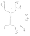
- Fiber optic coupler 1000 is illustrated in Fig. 10 in which two wavelengths ⁇ i and ⁇ j , are separated and supplied on respective outputs 1010 and 1020.
- a plurality of such fiber optic couplers can be cascaded in a manner similar to that shown in Fig. 9 to thereby demultiplex a plurality of wavelengths within a given group of channels.
- selectors 530 or 630 may be provided at the outputs of Mach-Zehnder interferometers 725, 730, 735 and 740 of Fig. 7, or at the outputs of the cascaded fiber optic couplers 1000, in order to reject any extraneous wavelengths, e.g., cross-talk.
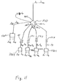
- Fig. 11 shows an alternative demultiplexer, whereby splitter 110 and filtering elements 125-1 to 125-3, 135-1 and 135-2 are replaced by five port circulator 1110 and in-fiber Bragg gratings 1111 to 1114 Channels ⁇ 1-40 are supplied to a first port 1110-1 of circulator 1110 and are output through port 1110-2.
- In-fiber Bragg grating 1114 is configured to transmit channels ⁇ 1-8 and reflect channels ⁇ 9-40 . Accordingly, channels ⁇ 1-8 are supplied to sub-demultiplexer 1120-1 for further demultiplexing while channels ⁇ 9-40 are reflected back to second port 1110-2 and output to port 1110-3.
- In-fiber Bragg grating 1113 which is coupled to second port 1110-3, is configured to reflect channels ⁇ 17-40 and transmit channels ⁇ 9-16 .
- channels ⁇ 9-16 are passed to sub-demultiplexer 1120-2 for further demultiplexing and channels ⁇ 17-40 are reflected back to port 1110-3 and output through port 1110-4.
- In-fiber Bragg gratings 1112 and 1111 coupled to corresponding ports 1110-4 and 1110-5, are configured to transmit channel groups ⁇ 17-24 and ⁇ 25-32 , respectively, and reflect the remaining channels.
- channel groups ⁇ 17-24 and ⁇ 25-32 are selected in a manner similar to that described above, and supplied to corresponding sub-demultiplexers 1120-3 and 1120-4 for further demultiplexing.
- channels ⁇ 33-40 are output through port 1110-6 and supplied to sub-demultiplexer 1120-5 for further demultiplexing.
- sub-demultiplexers 1120-1 to 1120-5 have a structure similar to that shown in Fig. 7.
- Fig. 12 illustrates optical multiplexer 1200 for multiplexing forty channels onto a single fiber 1205.
- each channel input to multiplexer 1200 is supplied on a respective input optical communication path or line to one of optical combiners 1211 to 1215.
- Optical combiners 1211 to 1215 can be similar to optical splitter 515, but with the inputs and outputs reversed.
- combiner 1211 receives channels ⁇ 1 - ⁇ 8 on respective input lines and combines these channels as a channel group onto a single output line 1231.
- channel groups ⁇ 9 - ⁇ 16 , ⁇ 17 - ⁇ 24 , ⁇ 25 - ⁇ 32 , and ⁇ 33 - ⁇ 40 are output from combiners 1212, 1213, 1214 and 1215 on lines 1232, 1233, 1234 and 1235, respectively.
- Lines 1231 and 1232 are fed to an additional combiner such as a filtering element 1221, commercially available from JDS Fitel or E-Tek, for example, for combining channel groups ⁇ 1 - ⁇ 8 and ⁇ 9 - ⁇ 16 onto line 1241.
- Lines 1234 and 1235 are coupled to filtering element 1223, which combines ⁇ 25 - ⁇ 32 and ⁇ 33 - ⁇ 40 onto a single line 1236, and lines 1233 and 1236 are fed to filtering element 1222, which combines channel groups ⁇ 17 - ⁇ 24 , ⁇ 25 - ⁇ 32 , ⁇ 33 - ⁇ 40 onto a single line 1242.
- Lines 1241 and 1242 are connected to coupler 1231, similar in construction to splitter 110 but having the inputs and outputs reversed, for combining channel groups ⁇ 1 - ⁇ 8 , ⁇ 9 - ⁇ 16 , ⁇ 17 - ⁇ 24 , ⁇ 25 - ⁇ 32 , and ⁇ 33 - ⁇ 40 onto line 1205.
- Optical multiplexer 1200 is readily expandable by adding additional combiners and filtering elements.
- Fig. 13 illustrates a multiplexer 1300, in accordance with the present invention, which can also multiplex a relatively large number of channels.
- Optical multiplexer 1300 is shown multiplexing 80 channels, but any appropriate number of channels can be suitably multiplexed with the multiplexer in accordance with the present invention.
- Multiplexer 1300 includes a plurality of conventional 1 x 8 combiners 1310-1 to 1310-10, for example, each having eight inputs receiving a respective one of eight channels.
- Combiners 1310-1 to 1310-10 can include one or more of the following: dielectric filters, fiber couplers, planar waveguides, arrayed waveguide routers, and appropriate combinations of fiber Bragg gratings and circulators.
- Combiners 1310-1 to 1310-10 combine the received channels onto corresponding outputs, which are coupled to respective optical attenuators 1312-1 to 1312-9.
- a series of cascaded combiners including for example optical filter elements 1314-1 to 1314-9, generally receive optical signal inputs from corresponding optical attenuators 1312-1 to 1314-9, and add these signals to signals input from a preceding optical filter element.
- filter element 1314-1 adds channels ⁇ 1 to ⁇ 8 received from combiner 1310-1 and channels ⁇ 9 to ⁇ 16 output from combiner 1310-2 via attenuator 1312-1.
- the aggregated channels, channels ⁇ 1 to ⁇ 16 are passed to filtering element 1314-2, which adds channels ⁇ 17 to ⁇ 24 output from attenuator 1312-2 thereto.
- channel groups ⁇ 25 to ⁇ 32 , ⁇ 33 to ⁇ 40 , ⁇ 41 to ⁇ 48 , ⁇ 56 to ⁇ 64 , and ⁇ 72 to ⁇ 80 are successively added by filters 1314-3 to 1314-9.
- the final filtering element stage 1314-9 outputs the entire aggregation of channels, ⁇ 1 to ⁇ 80 onto a single output fiber 1316.
- Filtering element 1314-1 has a similar construction as that shown in Fig. 2. For example, channels ⁇ 9 to ⁇ 16 are added to channels ⁇ 1 to ⁇ 8 by supplying channels ⁇ 9 to ⁇ 16 through port 1406 and channels ⁇ 1 to ⁇ 8 through port 1410. Channels ⁇ 9 to ⁇ 16 are emitted from an end of fiber 1422, collimated by lens 1424 and transmitted through dielectric filter 1414.
- Dielectric filter 1414 typically includes a transparent substrate coated with a plurality of dielectric layers configured to transmit, in this case, a band of wavelengths including channels ⁇ 9 to ⁇ 16 to lens 1412.
- Channels ⁇ 9 to ⁇ 16 are then focused onto an end of output fiber 1420.
- Channels ⁇ 1 to ⁇ 8 are emitted from an end of fiber 1408, collimated by lens 1412, and reflected dielectric filter 1414, which reflects wavelengths outside the ⁇ 9 to ⁇ 16 band.
- Channels ⁇ 1 to ⁇ 8 are next focused onto the end of output fiber 1420, and are thus added with channels ⁇ 9 to ⁇ 16 .
- Channels ⁇ 1 to ⁇ 8 incur a loss when combined with channels ⁇ 9 to ⁇ 16 in filtering element 1314-1, and experience further loss when combined with remaining channels ⁇ 17 to ⁇ 72 in filtering elements 1314-2 to 1314-9.
- channels ⁇ 9 to ⁇ 72 accumulate varying degrees of loss when output from combining filters 1314-2 to 1314-9.
- channels output from multiplexer 1300 have unequal optical power.
- substantially uniform channel power is desirable, because optical amplifiers downstream from the multiplexer may otherwise substantially degrade the optical signal-to-noise ratio of the low power channels.
- noise in a receiver can adversely affect detection of low power signals.
- Attenuators 1312-1 to 1312-9 are provided to impose an additional loss on channels input to filtering elements 1314-1 to 1314-9.
- the amount of attenuation for each attenuator is typically selected based on the number of filtering elements separating the attenuator from output fiber 1316. For example, the attenuation of attenuator 1312-1 is less than that of attenuators 1312-2 to 1312-9 because optical signals passing through attenuator 1312-1 will incur further loss passing through filtering elements 1314-2 to 1314-9.
- Attenuator 1312-9 is greater than that of the remaining attenuators so that substantially uniform optical power can be achieved for each channel output on fiber 1316.
- an attenuator may be provided at the output of combiner 1310-1, if necessary.
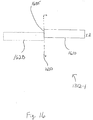
- optical attenuator 1312-1 will next be described with reference to Figs. 15 and 16. It is understood that optical attenuators 1312-2 to 1312-9 typically have a similar construction. Moreover, the structure of optical attenuator 1312-1 is exemplary, and other optical attenuator configurations are considered within the scope of the invention.
- optical attenuator 1312-1 includes two optical fibers 1610 and 1620 joined at respective end portions.
- fibers 1610 and 1620 further include core regions 1520 and 1510, and cladding regions 1530 and 1540, as commonly understood.
- the refractive indices of the core and cladding are selected so that light propagating through fibers 1610 and 1620 is confined to the cores thereof.
- the cores and claddings of both fibers are typically provided about respective axes, as is generally known.
- the axes and thus the cores of fibers 1610 and 1620 are offset from one another by a distance d.
- a portion of light passing from fiber 1620 to fiber 1610 is dispersed at interface 1635 of the two fibers, while the remaining portion of the light passes through fiber 1610.
- the amount of attenuation is determined by offset d; a relatively small offset distance d yields less attenuation while a greater offset distance provides more attenuation.
- offset distance d is adjusted for each of attenuators 1312-1 to 1312-9 so that a different attenuation can be obtained for each attenuator, and as discussed above, substantially equalized optical power can be achieved for each channel output from multiplexer 1300.
- fibers 1610 and 1620 are fusion spliced, so that outer surfaces of these fibers are smooth and continuous at interface 1630, as shown in Fig. 17.
- the cores of the fibers remain offset to provide a desired attenuation, as discussed above.
- Multiplexer 1300 has a relatively simple construction and does not require couplers, as is the case with multiplexer 1200 discussed above with reference to Fig. 12.
Landscapes
- Engineering & Computer Science (AREA)
- Computer Networks & Wireless Communication (AREA)
- Signal Processing (AREA)
- Optical Communication System (AREA)
Description
- The present application claims the benefit of U.S. Provisional Application Serial No.09/274,063, filed March 22, 1999.
- The present invention is directed to an optical multiplexer for multiplexing optical signals in a dense wavelength division multiplexed system.
- Optical communication systems are a substantial and fast growing constituent of communication networks. The expression "optical communication system," as used herein, relates to any system which uses optical signals to convey information across an optical waveguiding medium, for example, an optical fiber. Such optical systems include but are not limited to telecommunication systems, cable television systems, and local area networks (LANs). Currently, the many optical communication systems are configured to carry an optical channel of a single wavelength over one or more optical waveguides. To convey information from plural sources, time-division multiplexing is frequently empioyed (TDM). In time-division multiplexing, a particular time slot is assigned to each signal source, the complete signal being constructed from the portions of the signals collected from each time slot. While this is a useful technique for carrying plural information sources on a single channel, TDM capacity is limited by fiber dispersion and the need to generate high peak power pulses.
- While the need for communication services increases, the current capacity of existing waveguiding media is limited. Although capacity may be expanded e.g., by laying more fiber optic cables, the cost of such expansion is prohibitive. Consequently, there exists a need for a cost-effective way to increase the capacity of existing optical waveguides.
- Wavelength division multiplexing (WDM) has been explored as an approach for increasing the capacity of existing fiber optic networks. WDM systems typically include a plurality of transmitters, each respectively transmitting signals on a designated one of a plurality of channels or wavelengths. The channels are combined by a multiplexer at one end terminal and transmitted on a single fiber to a demultiplexer at another end terminal where they are separated and supplied to respective receivers.
- Recently, dense WDM (DWDM) systems transmitting 8 channels on a single fiber have been proposed. These systems can include a demultiplexer having a 1 x 8 optical splitter, which receives the 8 channels on an input fiber, and outputs the channels on each of 8 outputs. The power level on each of the outputs, however, is approximately 1/8 the input power level. Optical components are respectively coupled to the outputs of the 1 x 8 splitter for outputting a corresponding one of the 8 channels, which introduce additional loss.
- Although 8 channel WDM systems provide improved capacity, the need for additional capacity has increased with growing internet traffic and demand for multimedia services. Thus, DWDM systems having higher channel counts are currently being developed. In high channel count systems, however, it is difficult to multiplex and demultiplex a large number of optical channels. For example, in a 40 channel DWDM system, a 1 x 40 splitter would be inadequate to demultiplex each of the channels because the power level at each output of such a splitter would be insufficient to maintain an adequate signal to noise ratio. As a result, the transmitted channels cannot be adequately detected. On the other hand, although an optical amplifier could be used to increase the power on the input of the 1 x 40 splitter, such an amplifier can be difficult to manufacture, and would fail to provide the requisite optical power per channel at higher channel counts. Moreover, if amplifiers were to be provided at each of the outputs of the 1 x 40 splitter, the cost of the demultiplexer would be excessive. WO 99/13607 A discloses an optical multiplexer for multiplexing forty channels onto a single fiber.
- Thus, there is a need for a multiplexer and demultiplexer suitable for incorporation into a high channel count DWDM system which minimizes power loss and enables adequate detection of the transmitted channels. There is also a need for a scaleable DWDM system, which can readily accommodate additional channels with minimal expense.
- According to an aspect of the present invention, an optical device is provided as claimed in
claim 1. According to a further aspect of the invention there is provided a method for multiplexing optical signals as claimed in claim 15. The present invention is characterised over WO 99/13607 A by the characterising portions ofclaims 1 and 15. There is also described herein an optical splitter having an input and first and second outputs. The input of the optical splitter is coupled to an input optical path, which carries a plurality of optical channels. Each of the optical channels has a respective wavelength. The first output of the optical splitter being coupled to a first output optical path, and the second output being coupled to a second output optical path, with the first and second output optical paths each carrying the plurality of optical channels. - The optical device consistent with the present invention further comprises a first optical filtering element coupled to the first output optical path for selecting a first group of said plurality of optical channels; and a second optical filtering element coupled to the second output optical path for selecting a second group of said plurality of optical channels. A first optical demultiplexer is coupled to the first optical filtering element and includes a plurality of outputs. A corresponding one of the first group of channels appearing on a respective one of the plurality of outputs of said first optical demultiplexer. Further, a second optical demultiplexer is coupled to the second optical filtering element. The second optical demultiplexer comprises a plurality of outputs, a corresponding one of the second group of channels appearing on a respective one of the plurality of outputs of the second optical demultiplexer.
- Advantages of the present invention will be apparent from the following detailed description of the presently preferred embodiments thereof, which description should be considered in conjunction with the accompanying drawings in which:
- Fig. 1 illustrates a schematic diagram of an optical demultiplexer;
- Fig. 2 illustrates a schematic diagram of an interference filter;
- Fig. 3 illustrates transmittance characteristics of filtering elements 125-1, 125-2 and 125-3 shown in Fig. 1;
- Fig. 4 illustrates transmittance characteristics of filtering elements 130-1 and 130-2 shown in Fig. 1;
- Fig. 5 illustrates plots of loss vs. channel count for the present invention and a conventional demultiplexer;
- Fig. 6 illustrates an additional example of a demultiplexer;
- Fig. 7 illustrates an example of a sub-demultiplexer;
- Fig. 8 illustrates an additional example of a sub-demultiplexer;
- Fig. 9 illustrates a further example of a sub-demultiplexer;
- Fig. 10 illustrates a fiber optic coupler demultiplexer for separating two wavelengths;
- Fig. 11 illustrates an additional example of a demultiplexer;
- Fig. 12 illustrates an optical multiplexer;
- Fig. 13 illustrates an optical multiplexer in accordance with the present invention;
- Fig. 14 illustrates a filtering element shown in Fig. 13;
- Fig. 15 illustrates a cross-sectional view of an exemplary optical attenuator shown in Fig. 13;
- Fig. 16 illustrates a side view of an optical attenuator shown in Fig. 15; and
- Fig. 17 illustrates a side view of the optical attenuator after fusion splicing.
- In accordance with an arrangement described herein, optical channels to be demultiplexed are supplied to first and second optical fibers via an optical splitter. Low loss interference filters, for example, coupled to the first and second optical fibers, select respective groups of channels. Each group of channels is next demultiplexed with sub-demultiplexers into individual channels, each of which is then sensed with a corresponding photodetector. Although the optical splitter introduces an optical power loss at the input to the demultiplexer, the interference filters and sub-demultiplexers create little additional loss. As a result, the total power loss associated with the present invention is significantly less than that obtained with a conventional n channel demultiplexer based on a 1 x n splitter. Accordingly, large numbers of channels, e.g., in excess of forty can be readily demultiplexed and detected.
- Turning to the drawings in which like reference characters indicate the same or similar elements in each of the several views, Fig. 1 illustrates
optical demultiplexer 100 consistent with the present invention. As discussed in greater detail below, the exemplary demultiplexer illustrated in Fig. 1 demultiplexes 40 channels. The present invention, however, is not limited to this number of channels. Rather, the present invention is applicable to demultiplexers that can separate any appropriate number of optical channels. - Returning to Fig. 1,
optical demultiplexer 100 receives, for example, a plurality of multiplexed optical channels λ1 - λ40 on inputoptical fiber 105. The multiplexed channels are emitted by laser transmitters (not shown) coupled tooptical fiber 105. The multiplexed channels are supplied to the input ofoptical splitter 110, which supplies channels λ1 - λ40 to first andsecond output fibers optical amplifier 101 may be provided at the input ofsplitter 110 in order to offset any loss introduced bysplitter 110. Alternatively, the loss imposed bysplitter 110 can be compensated by coupling optical amplifiers tooutput fibers - As further shown in Fig. 1, first optical filtering elements 125-1 to 125-3 are coupled to
first output fiber 120, and second filtering elements 130-1 and 130-2 are coupled tosecond output fiber 115. Each of these filtering elements typically includes an interference filter commercially available from JDS Fitel or DiCon, for example. - A simplified diagram of filtering element 125-1 incorporating an interference filter, for example, is illustrated in Fig. 2. Filtering element 125-1 receives channels λ1-λ40 on
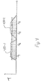
input fiber 210 having an end portion spaced from graded refractive index (GRIN)lens 215. As a result, light emitted from the end portion diverges prior to impinging onlens 215. Channels λ1-λ40 are collimated bylens 215 and directed toward dielectricthin film filter 220.Thin film filter 220 includes a substrate coated with a plurality of thin dielectric films of appropriate thickness and number to pass, in this case, channels λ1-λ8, and reflect channels λ17-λ40. Channels λ1-λ8 are thus transmitted to GRIN lens 218 where they are focused onto an end portion ofoutput fiber 235 and transmitted to a corresponding sub-demultiplexer via output port 240 of filtering element 125-1. Channels λ9-λ40, however, are reflected back toGRIN lens 215, focused ontofiber 225 and output throughport 230 to filtering element 125-2, which along with filtering element 125-3, typically has a similar construction as filtering element 125-1. - The transmittance vs. wavelength characteristics of filtering elements 125-1 to 125-3 are shown in Fig. 3. Transmittance band 325-1 of filtering element 125-1 has a relatively high transmittance over a range of wavelengths including the first eight channels, λ1-λ8. As noted above, therefore, these channels are transmitted toward an output port of filtering element 125-1. It should be noted, however, that channels λ9-λ11, for example, are also transmitted, but only partially, since they lie in the roll-off
region 324 of transmittance band 325-1. Remaining channels λ12-λ40, as well as channels λ9-λ11 at a substantially reduced power level, are reflected to filtering element 125-2 having high transmittance band 325-2. As a result, channels λ17-λ24 are transmitted toward the output port of filtering element 125-2. As further shown in Fig. 3, however, channels λ25-λ27, for example, adjacent λ17-λ24 are also transmitted, but to a lesser extent. Remaining channels λ28-λ40 are reflected and output to filtering element 125-3 of which channels λ33-λ40 fall within high transmittance band 325-3 and are thus passed to an output port of filtering element 125-3. Channels λ28-λ31, however, are partially transmitted. - As further shown in Fig. 1, channel groups λ1-λ8, λ17-λ24, and λ33-λ40 are respectively directed to sub-demultiplexers 135-1, 135-2 and 135-3 where further demultiplexing is performed to output individual channels on corresponding output ports. These output ports, in turn, are coupled to respective ones of
photodiodes 150 where the channels are converted into electrical signals for processing by appropriate circuitry (not shown). The term sub-demultiplexer is used herein to describe an optical apparatus that demultiplexes the groups of channels respectively output from the filtering elements. Sub-demultiplexers 135-1, 135-2 and 135-3 are discussed in greater detail below. - As noted above, channels lying outside the high transmittance bands of filtering elements 125-1, 125-2 and 125-3 are only partially reflected due to the relatively broad roll-off regions of the transmittance characteristics of interference filters, for example. Accordingly, channels adjacent the intended channel sub-groups incur a significant amount of power loss and cannot be effectively demultiplexed. These channels are therefore supplied by filtering elements 130-1 and 130-2 coupled to
second output fiber 115, as discussed in greater detail below with reference to Fig. 4. - As shown in Fig. 4, filtering element 130-1 has high transmittance band 430-1 extending over wavelengths λ9-λ16. Filtering element 130-1 typically has a similar construction to filtering element 125-1, and therefore transmits channels λ9-λ16 for output to corresponding sub-demultiplexer 140-1 and further demultiplexing. Remaining channels λ1-λ8 and λ17-λ40 are reflected to filtering element 130-2 having high transmittance band 430-2 encompassing channels λ25-λ32. Accordingly, channels λ25-λ32 are transmitted through filtering element 130-2 and directed toward sub-demultiplexer 140-2 for further demultiplexing into individual channels.
- Channels lying adjacent the high transmitttance bands 430-1 and 430-2, like those channels discussed previously adjacent high reflectance bands 325-1 to 325-3, are partially transmitted by filtering elements 130-1 and 130-2 and are thus difficult to detect after further demultiplexing. These channels, however, lie within the high transmittance bands of filtering elements 125-1 to 125-3 and are thus demultiplexed through sub-demultiplexers 135-1 to 135-3, respectively, as noted above. Therefore, in the presently described example of the present invention,
first output fiber 120, filtering elements 125-1 to 125-3 and corresponding sub-demultiplexers 135-1 to 135-3, serve to demultiplex channels λ1-λ8, λ17-λ24 and λ33-λ40, respectively. Additionally,second output fiber 120, filtering elements 130-1 and 130-2 and corresponding sub-demultiplexers 140-1 and 140-2 serve to demultiplex channels λ9-λ16 and λ25-λ32, respectively. Accordingly, alternating groups of channels are respectively selected by filtering elements 125-1 to 125-3 and 135-1 to 135-3. - Alternatively, if only 40 channels are to be separated by the demultiplexer in accordance with the present invention, filtering elements 130-2 and 125-3 can be omitted and sub-demultipelxers 140-2 and 135-3 can be coupled directly to the outputs of filtering elements 130-1 and 125-2, respectively.
- Filtering elements 125-1 to 125-3, 130-1 and 130-2 introduce little power loss to the selected sub-groups of channels. For example, the power loss associated with the channels reflected by the filtering elements is typically about 0.5 dB, and the loss associated with the channels transmitted through the filtering elements is about 0.7 dB. Thus, the overall loss of the demultiplexer is significantly reduced.
- It is noted that as the channels propagate down one of
output fibers output fibers - Fig. 5 illustrates loss L as a function of channel count n (curve 910) and a conventional 1 x n splitter based demultiplexer (curve 920). As seen in Fig. 5, at low channel counts, the loss associated with the demultiplexer described herein is higher than the conventional demultiplexer. This is due to the loss introduced by the 1 x 2
splitter 110, which imposes a minimum loss in the demultiplexer. At higher channel counts, however, the loss associated with the conventional demultiplexer increases linearly with n (curve 920). On the other hand, the loss associated with the demultiplexer described herein (curve 910) is stepped and increases at a much more gradual rate due, at least in part, to the low loss of the filtering elements. Therefore, at higher channel counts, channels demultiplexed as described experience less loss than those demultiplexed with a conventional 1 x n splitter. - Fig. 6 illustrates an alternative arrangement in which each filtering element constitutes a combination of a circulator and grating. In particular, filtering element 130-1 includes a circulator 830-1 receiving channels λ1-40 at a first circulator port 831-1 coupled to
output fiber 115. These channels are circulated to port 831-2 and output to in-fiber Bragg grating 832-1, which is configured to have a high reflectivity band that coincides with the band of channels λ9-16. Accordingly, channels λ9-16 are reflected back to port 831-2 while the remaining channels are transmitted to circulator 830-2. Channels λ9-16 are then circulated to output port 831-3 and supplied to a corresponding sub-demultiplexer. In a similar fashion circulators 830-2, 825-1, 825-2 and 825-3 output channel groups λ25-32, λ1-8, λ17-24 and λ33-40 in conjunction with in-fiber Bragg gratings 832-2, 832-3, 832-4, and 832-5, respectively. - Typically, in-fiber Bragg gratings 832-3, 832-4 and 832-5 reflect successively lower bands or wavelengths, such that the wavelengths in channel group λ1-8 are greater than the wavelengths in channel group λ17-24, and the wavelengths in channel group λ17-24 are greater than the wavelengths in channel group λ33-40. Further, in-fiber Bragg gratings 831-1 and 832-2 reflect successively lower bands of wavelengths. As a result, the demultiplexer shown in Fig. 6 avoids cladding or radiation mode loss.
- Examples of sub-demultiplexers will next be described with reference to Figs. 7-10. Although exemplary configurations are discussed in detail with respect to sub-demultiplexer 135-1, it is understood that the remaining sub-demultiplexers described above can have a similar structure. Moreover, the demultiplexer described herein is not limited to these specific sub-demultiplexer configurations nor the specific number of inputs and outputs disclosed. Rather, it is understood that any optically demultiplexing component capable of demultiplexing a group of channels can be used.
- Fig. 7 illustrates a first exemplary construction of sub-demultiplexer 135-1. As shown in Fig. 7, sub-demultiplexer 135-1 receives channels λ1-λ8 at an
input 525 of a 1 x 8splitter 515, commercially available from IOT, for example.Splitter 515 has eight outputs, each of which supplying channels λ1-λ8 to a corresponding one of eightoptical selectors 530.Splitter 515, as well assplitter 110, may include a waveguide doped with an optically active material, such as erbium. Such a waveguide may further be optically pumped so thatsplitter 515 has reduced loss or provides optical gain. - In Fig. 7, only one of the selectors is shown including a three
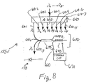
port circulator 510 having a first port 510-1 for receiving channels λ1-λ8 from one of the outputs ofsplitter 515. These channels are transmitted to in-fiber Bragg grating 520 via second port 510-2 ofcirculator 510. Typically, in-fiber Bragg grating 520 has a reflectance characteristic as a function of wavelength such that a reflectivity maximum is obtained at a desired channel or wavelength, e.g., λ1. Thus, only channel λ1 is reflected back to second port 510-2 and circulated to third circulator port 510-3, which outputs channel λ1 to one ofphotodiodes 150 for subsequent detection and further processing. Likewise, the in-fiber Bragg gratings in the remaining selectors have reflectivity maxima that respectively reflect a corresponding one of each of remaining wavelengths λ2-λ8 for output to one ofphotodiodes 150. - Fig. 8 illustrates an alternative construction for sub-demultiplexer 135-1. Here, the channel group λ1-λ8 is supplied to a planar arrayed waveguide grating (AWG) 610 or dielectric thin film demultiplexer, which supplies a respective channel on each of outputs 610-1 to 610-8. If the spacing between adjacent ones of channels λ1-λ8 is relatively narrow, AWG 610 can introduce an unacceptably high level of undesired cross-talk. Accordingly, additional filtering may be required. Thus, a
selector 630 is further illustrated in Fig. 8 to isolate a single channel, e.g., λ1, and remove any cross-talk. In this case,selector 630 includes acoupler 655 receiving substantially channel λ1 at a first port 655-1. The input light is next supplied to in-fiber Bragg grating 640 through second port 655-2. In-fiber Bragg grating 640 substantially reflects only channel λ1, while passing other wavelengths. Thus, channel λ1 is reflected back to second port 655-2 and output to one ofphotodiodes 150 via third output port 655-3 ofcoupler 655. - As further shown in Fig. 8,
feedback circuit 670 is optionally provided to insure that grating 640 reflects at the intended wavelengths. As is generally understood, an in-fiber Bragg grating typically includes a periodic variation of index of refraction, with the spacing between refractive index peaks defining, in part, the wavelength to be reflected by the grating. Variations in the wavelength of light reflected by grating 640 can be sensed withphotodiode 660, which supplies an electrical signal to afeedback circuit 670.Feedback circuit 670, in turn, generates an appropriate voltage signal to adjust a temperature regulator coupled to grating 640. Since the grating refractive index spacing changes with temperature, the temperature of the grating is set byfeedback circuit 670 to alter the grating spacing so that grating 640 reflects a desired wavelength. - Fig. 9 illustrates a further exemplary construction of sub-demultiplexer 135-1. In this instance, sub-demultiplexer 135-1 comprises a plurality of Mach-Zehnder interferometers. It is known that Mach-Zehnder interferometers, which include optical waveguides of varying lengths, can be used to separate wavelengths (see for example, published European Patent Application EP0482461). Accordingly, as shown in Fig. 9, Mach-Zehnder interferometers can be cascaded to separate a group of wavelengths. For example, Mach-
Zehnder interferometer 710 separates input channels λ1-λ8 into sub-groups of channels λ1, 3, 5, 7 and λ2, 4, 6, 8, respectively. Channel sub-group λ1, 3, 5, 7 is supplied to Mach-Zehnder interferometer 715 and channel sub-group λ2, 4, 6, 8 is supplied to Mach-Zehnder interferometer 720. As further shown in Fig. 9, Mach-Zehnder interferometers 715 and 720 further break down these channel sub-groups to channel pairs λ1,5, λ3,7, λ2,6, and λ4.8, which are further demultiplexed into individual channels by Mach-Zehnder interferometers - Fiber optical couplers, commercially available from Applied Fiber Optics, Inc. and Gould, for example, can also be used to demultiplex the groups of channels supplied by the filtering elements.
Fiber optic coupler 1000 is illustrated in Fig. 10 in which two wavelengths λi and λj, are separated and supplied onrespective outputs 1010 and 1020. A plurality of such fiber optic couplers can be cascaded in a manner similar to that shown in Fig. 9 to thereby demultiplex a plurality of wavelengths within a given group of channels. If necessary,selectors Zehnder interferometers fiber optic couplers 1000, in order to reject any extraneous wavelengths, e.g., cross-talk. - Fig. 11 shows an alternative demultiplexer, whereby
splitter 110 and filtering elements 125-1 to 125-3, 135-1 and 135-2 are replaced by fiveport circulator 1110 and in-fiber Bragg gratings 1111 to 1114 Channels λ1-40 are supplied to a first port 1110-1 ofcirculator 1110 and are output through port 1110-2. In-fiber Bragg grating 1114 is configured to transmit channels λ1-8 and reflect channels λ9-40. Accordingly, channels λ1-8 are supplied to sub-demultiplexer 1120-1 for further demultiplexing while channels λ9-40 are reflected back to second port 1110-2 and output to port 1110-3. In-fiber Bragg grating 1113, which is coupled to second port 1110-3, is configured to reflect channels λ17-40 and transmit channels λ9-16. As a result, channels λ9-16 are passed to sub-demultiplexer 1120-2 for further demultiplexing and channels λ17-40 are reflected back to port 1110-3 and output through port 1110-4. - In-fiber Bragg gratings 1112 and 1111, coupled to corresponding ports 1110-4 and 1110-5, are configured to transmit channel groups λ17-24 and λ25-32, respectively, and reflect the remaining channels. Thus, channel groups λ17-24 and λ25-32 are selected in a manner similar to that described above, and supplied to corresponding sub-demultiplexers 1120-3 and 1120-4 for further demultiplexing. In addition, channels λ33-40 are output through port 1110-6 and supplied to sub-demultiplexer 1120-5 for further demultiplexing. Typically, sub-demultiplexers 1120-1 to 1120-5 have a structure similar to that shown in Fig. 7.
- Fig. 12 illustrates optical multiplexer 1200 for multiplexing forty channels onto a
single fiber 1205. As seen in Fig. 12, each channel input to multiplexer 1200 is supplied on a respective input optical communication path or line to one ofoptical combiners 1211 to 1215.Optical combiners 1211 to 1215 can be similar tooptical splitter 515, but with the inputs and outputs reversed. As further shown in Fig. 12,combiner 1211 receives channels λ1-λ8 on respective input lines and combines these channels as a channel group onto asingle output line 1231. Likewise, channel groups λ9-λ16, λ17-λ24, λ25-λ32, and λ33-λ40 are output fromcombiners lines Lines filtering element 1221, commercially available from JDS Fitel or E-Tek, for example, for combining channel groups λ1-λ8 and λ9-λ16 ontoline 1241.Lines filtering element 1223, which combines λ25-λ32 and λ33-λ40 onto asingle line 1236, andlines filtering element 1222, which combines channel groups λ17-λ24, λ25-λ32, λ33-λ40 onto asingle line 1242.Lines coupler 1231, similar in construction tosplitter 110 but having the inputs and outputs reversed, for combining channel groups λ1-λ8, λ9-λ16, λ17-λ24, λ25-λ32, and λ33-λ40 ontoline 1205. - Optical multiplexer 1200 is readily expandable by adding additional combiners and filtering elements.
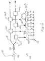
- Fig. 13 illustrates a
multiplexer 1300, in accordance with the present invention, which can also multiplex a relatively large number of channels.Optical multiplexer 1300 is shown multiplexing 80 channels, but any appropriate number of channels can be suitably multiplexed with the multiplexer in accordance with the present invention. - Multiplexer 1300 includes a plurality of conventional 1 x 8 combiners 1310-1 to 1310-10, for example, each having eight inputs receiving a respective one of eight channels. Combiners 1310-1 to 1310-10 can include one or more of the following: dielectric filters, fiber couplers, planar waveguides, arrayed waveguide routers, and appropriate combinations of fiber Bragg gratings and circulators. Combiners 1310-1 to 1310-10 combine the received channels onto corresponding outputs, which are coupled to respective optical attenuators 1312-1 to 1312-9. A series of cascaded combiners, including for example optical filter elements 1314-1 to 1314-9, generally receive optical signal inputs from corresponding optical attenuators 1312-1 to 1314-9, and add these signals to signals input from a preceding optical filter element. In particular, filter element 1314-1 adds channels λ1 to λ8 received from combiner 1310-1 and channels λ9 to λ16 output from combiner 1310-2 via attenuator 1312-1. The aggregated channels, channels λ1 to λ16, are passed to filtering element 1314-2, which adds channels λ17 to λ24 output from attenuator 1312-2 thereto. In a similar fashion channel groups λ25 to λ32, λ33 to λ40, λ41 to λ48, λ56 to λ64, and λ72 to λ80 are successively added by filters 1314-3 to 1314-9. The final filtering element stage 1314-9 outputs the entire aggregation of channels, λ1 to λ80 onto a single output fiber 1316.
- An exemplary filtering element 1314-1 is illustrated in greater detail in Fig. 14. Filtering element 1314-1 has a similar construction as that shown in Fig. 2. For example, channels λ9 to λ16 are added to channels λ1 to λ8 by supplying channels λ9 to λ16 through
port 1406 and channels λ1 to λ8 throughport 1410. Channels λ9 to λ16 are emitted from an end offiber 1422, collimated bylens 1424 and transmitted throughdielectric filter 1414.Dielectric filter 1414 typically includes a transparent substrate coated with a plurality of dielectric layers configured to transmit, in this case, a band of wavelengths including channels λ9 to λ16 tolens 1412. Channels λ9 to λ16 are then focused onto an end ofoutput fiber 1420. Channels λ1 to λ8, however, are emitted from an end offiber 1408, collimated bylens 1412, and reflecteddielectric filter 1414, which reflects wavelengths outside the λ9 to λ16 band. Channels λ1 to λ8 are next focused onto the end ofoutput fiber 1420, and are thus added with channels λ9 to λ16. - Channels λ1 to λ8, however, incur a loss when combined with channels λ9 to λ16 in filtering element 1314-1, and experience further loss when combined with remaining channels λ17 to λ72 in filtering elements 1314-2 to 1314-9. Likewise, channels λ9 to λ72 accumulate varying degrees of loss when output from combining filters 1314-2 to 1314-9. Thus, in the absence of attenuators 1312-1 to 1312-9, channels output from
multiplexer 1300 have unequal optical power. In WDM systems, however, substantially uniform channel power is desirable, because optical amplifiers downstream from the multiplexer may otherwise substantially degrade the optical signal-to-noise ratio of the low power channels. In addition, noise in a receiver can adversely affect detection of low power signals. - In order to insure, therefore, that each channel output from
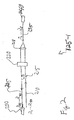
multiplexer 1300 has substantially the same optical power, attenuators 1312-1 to 1312-9 are provided to impose an additional loss on channels input to filtering elements 1314-1 to 1314-9. The amount of attenuation for each attenuator is typically selected based on the number of filtering elements separating the attenuator from output fiber 1316. For example, the attenuation of attenuator 1312-1 is less than that of attenuators 1312-2 to 1312-9 because optical signals passing through attenuator 1312-1 will incur further loss passing through filtering elements 1314-2 to 1314-9. In contrast, since optical signals output from combiner 1310-10 do not pass through a series of dielectric filters and thus experience relatively little loss, the attenuation associated with attenuator 1312-9 is greater than that of the remaining attenuators so that substantially uniform optical power can be achieved for each channel output on fiber 1316. Optionally, an attenuator may be provided at the output of combiner 1310-1, if necessary. - Optical attenuator 1312-1 will next be described with reference to Figs. 15 and 16. It is understood that optical attenuators 1312-2 to 1312-9 typically have a similar construction. Moreover, the structure of optical attenuator 1312-1 is exemplary, and other optical attenuator configurations are considered within the scope of the invention.
- As seen in Fig. 16, optical attenuator 1312-1 includes two
optical fibers line 1630,fibers core regions cladding regions fibers - As further shown in Figs. 15 and 16, the axes and thus the cores of
fibers fiber 1620 tofiber 1610, for example, is dispersed atinterface 1635 of the two fibers, while the remaining portion of the light passes throughfiber 1610. As a result, light transmitted throughinterface 1635 experiences loss, and is thus attenuated. The amount of attenuation is determined by offset d; a relatively small offset distance d yields less attenuation while a greater offset distance provides more attenuation. - Typically, offset distance d is adjusted for each of attenuators 1312-1 to 1312-9 so that a different attenuation can be obtained for each attenuator, and as discussed above, substantially equalized optical power can be achieved for each channel output from
multiplexer 1300. - Typically,
fibers interface 1630, as shown in Fig. 17. The cores of the fibers, however, remain offset to provide a desired attenuation, as discussed above. - Multiplexer 1300 has a relatively simple construction and does not require couplers, as is the case with multiplexer 1200 discussed above with reference to Fig. 12.
- While the foregoing invention has been described in terms of the embodiments discussed above, numerous variations are possible. Accordingly, modifications and changes such as those suggested above, but not limited thereto, are considered to be within the scope of the following claims.
Claims (15)
- An optical device (1300) comprising:a first optical combiner (1310-2, ..., 1310-10) for receiving a first plurality of optical signals, each of which being at a respective one of a first plurality of wavelengths, said first optical combiner (1310-2, ..., 1310-10) having an output for supplying said first plurality of optical signals to an optical communication path; and characterised in that it comprises:a first optical attenuator (1312-1, ..., 1312-9) coupled to said optical communication path, said first optical attenuator (1312-1, ..., 1312-9) having an input for receiving said first plurality of optical signals and an output for supplying said first plurality of optical signals in attenuated form; anda second optical combiner (1314-1, ..., 1314-9) having a first input coupled to said output of said first attenuator (1312-1, ..., 1312-9) and for receiving said attenuated first plurality of optical signals, and a second input for receiving a second plurality of optical signals, each of said second plurality of optical signals being at a respective one of a second plurality of wavelengths, said second optical combiner having an output for supplying said first and second pluralities of optical signals, wherein each optical signal within said first and second pluralities of optical signals output from said second optical combiner has substantially uniform optical power.
- An optical device (1300) in accordance with claim 1, wherein said second optical combiner (1314-1, ..., 1314-9) comprises a dielectric filter (1414).
- An optical device (1300) in accordance with claim 1, wherein said first optical attenuator (1312-1, ..., 1312-9) comprises:a first optical fiber (1610) having a core portion (1510) and a cladding portion (1540), said core (1510) and cladding (1640) of said first optical fiber (1610) being disposed about a first axis; anda second optical fiber (1620) having a core portion (1520) and a cladding portion (1530), said core (1520) and said cladding (1530) of said second optical fiber (1620) being disposed about a second axis, said first and second optical fibers (1610, 1620) being joined at respective ends thereof such that said first axis is offset from said second axis.
- An optical device (1300) in accordance with claim 1, further comprising a third optical combiner (1314-1, ..., 1314-8), said third optical combiner receiving each of said second plurality of optical signals, and having an output for supplying said second plurality of optical signals, said output of said third optical combiner being coupled to said second input of said second optical combiner (1314-1, ..., 1314-9).
- An optical device (1300) in accordance with claim 1, further comprising:a third optical combiner (1310-3, ..., 1310-10) having a plurality of inputs, each of which receiving a respective one of a third plurality of optical signals, each of said third plurality of optical signals being at a respective one of a third plurality of wavelengths, said third optical combiner (1310-3, ..., 1310-10) having an output supplying said third plurality of optical signals;a second optical attenuator (1312-2, ..., 1312-9) coupled to said output of said third optical combiner (1310-3, ..., 1310-10), said second optical attenuator (1312-2, ..., 1312-9) having an input receiving said third plurality of optical signals and an output supplying said third plurality of optical signals in attenuated form; anda fourth optical combiner (1314-2, ..., 1314-9) having a first input coupled to said output of said second optical attenuator (1312-2, ..., 1312-9), a second input coupled to said output of said second optical combiner (1314-1, ..., 1314-8) and receiving said first and second pluralities of optical signals, and an output supplying said first, second and third pluralities of optical signals.
- An optical device (1300) in accordance with claim 5, wherein said second and fourth optical combiners each include a dielectric filter (1414).
- An optical device (1300) in accordance with claim 5, wherein said first optical attenuator (1312-1, ..., 1312-8) comprises:a first optical fiber (1610) having a core portion (1510) and a cladding portion (1540), said core and cladding of said first optical fiber (1610) being disposed about a first axis; anda second optical fiber (1620) having a core portion (1520) and a cladding portion (1530), said core and said cladding of said second optical fiber (1620) being disposed about a second axis, said first and second optical fibers being joined at respective ends thereof such that said first axis is offset from said second axis by a first distance.
- An optical device (1300) in accordance with claim 7, wherein said second optical attenuator (1312-2, ..., 1312-9) comprises:a third optical fiber (1610) having a core portion (1510) and a cladding portion (1540), said core and cladding of said third optical fiber (1610) being disposed about a third axis; anda fourth optical fiber (1620) having a core portion (1520) and a cladding portion (1530), said core and said cladding of said fourth optical fiber (1620) being disposed about a fourth axis, said third and fourth optical fibers being joined at respective ends thereof such that said third axis is offset from said fourth axis by a second distance, said first distance being different than said second distance.
- An optical device (1300) in accordance with claim 5, wherein an attenuation associated with said first optical attenuator (1312-1, ..., 1312-8) is different than an attenuation associated with said second optical attenuator (1312-2, ..., 1312-9).
- An optical device (1300) in accordance with claim 1, wherein:said first optical combiner is one of a first plurality of optical combiners (1310-2, ..., 1310-10), each of which receiving a respective one of a plurality of groups of optical signals, each optical signal within each of said plurality of groups being at a different wavelength, each of said first plurality of optical combiners (1310-2, ..., 1310-10) having a respective output for supplying corresponding ones of said plurality of groups of optical signals;said first optical attenuate is one of a plurality of optical attenuators each of which being associated with a corresponding one of said first plurality of optical combiners, each of said plurality of optical attenuators (1312-1, ..., 1312-9) supplying a corresponding one of said plurality of groups of optical signals through a respective output; andsaid second optical combiner is one ofa second plurality of optical combiners, each of which being coupled to a respective one of said plurality of optical attenuators, each of said second plurality of optical combiners (1314-1, ..., 1314-9) having a first input receiving a first one of said plurality of groups of optical signals from a corresponding one of said plurality of optical attenuators, a second input receiving at least a second, different one of said plurality of groups of optical signals, and an output supplying said first one of said plurality of groups of optical signals and said second, different one of said plurality of groups of optical signals.
- An optical device (1300) in accordance with claim 10, wherein each of said second plurality of optical combiners (1314-1, ..., 1314-9) comprises a dielectric filter (1414).
- An optical device (1300) in accordance with claim 10, wherein each of said optical signals output from one of said second plurality of optical combiners (1314-1, ..., 1314-9) has substantially uniform optical power.
- An optical communication device (1300) in accordance with claim 12, wherein each of said plurality of optical attenuators (1312-1, ..., 1312-9) comprises:a first optical fiber (1610) having a core portion (1510) and a cladding portion (1540), said core and cladding of said first optical fiber (1610) being disposed about a first axis; anda second optical fiber (1620) having a core portion (1520) and a cladding portion (1530), said core and said cladding of said second optical fiber (1620) being disposed about a second axis, said first and second optical fibers being joined at respective ends thereof such that said first axis is offset from said second axis by an offset distance.
- An optical device in accordance with claim 13, wherein said offset distance is different for each of said plurality of optical attenuators (1312-1, ..., 1312-9).
- A method for multiplexing optical signals, comprising :combining a first plurality of optical signals onto a single optical communication path; and characterised by the steps of :attenuating said combined optical signals; andcombining a second plurality of optical signals with said attenuated first plurality of optic al signals, whereby each optical signal within said attenuated first plurality and said second plurality of optical signals has substantially uniform optical power.
Applications Claiming Priority (3)
| Application Number | Priority Date | Filing Date | Title |
|---|---|---|---|
| US274063 | 1999-03-22 | ||
| US09/274,063 US6567196B1 (en) | 1999-03-22 | 1999-03-22 | Dense WDM optical multiplexer and demultiplexer |
| PCT/US2000/007565 WO2000057590A1 (en) | 1999-03-22 | 2000-03-22 | Dense wdm optical multiplexer and demultiplexer |
Publications (2)
| Publication Number | Publication Date |
|---|---|
| EP1078487A1 EP1078487A1 (en) | 2001-02-28 |
| EP1078487B1 true EP1078487B1 (en) | 2006-03-08 |
Family
ID=23046603
Family Applications (1)
| Application Number | Title | Priority Date | Filing Date |
|---|---|---|---|
| EP00918235A Expired - Lifetime EP1078487B1 (en) | 1999-03-22 | 2000-03-22 | Dense wdm optical multiplexer and demultiplexer |
Country Status (5)
| Country | Link |
|---|---|
| US (1) | US6567196B1 (en) |
| EP (1) | EP1078487B1 (en) |
| CA (1) | CA2333057A1 (en) |
| DE (1) | DE60026497T2 (en) |
| WO (1) | WO2000057590A1 (en) |
Cited By (1)
| Publication number | Priority date | Publication date | Assignee | Title |
|---|---|---|---|---|
| US11272269B1 (en) | 2021-03-29 | 2022-03-08 | Ciena Corporation | Integrated band splitter for scaling dual-band ROADM |
Families Citing this family (21)
| Publication number | Priority date | Publication date | Assignee | Title |
|---|---|---|---|---|
| US6721508B1 (en) | 1998-12-14 | 2004-04-13 | Tellabs Operations Inc. | Optical line terminal arrangement, apparatus and methods |
| US6968130B1 (en) * | 1999-09-07 | 2005-11-22 | Nokia Corporation | System and method for fully utilizing available optical transmission spectrum in optical networks |
| US6760532B1 (en) * | 2000-01-28 | 2004-07-06 | Ciena Corporation | Optical device having dynamic channel equalization |
| WO2002011337A1 (en) * | 2000-07-31 | 2002-02-07 | Mitsubishi Denki Kabushiki Kaisha | Optical wavelength division multiplexing device |
| EP1378082A2 (en) * | 2001-04-03 | 2004-01-07 | Nortel Networks Limited | High spectral efficiency, high performance optical mux and demux architecture |
| US7340174B2 (en) | 2001-12-28 | 2008-03-04 | Nortel Networks Limited | Programmable OADM with chromatic dispersion, dispersion slope and amplitude ripple compensation, and method |
| JP2003185876A (en) * | 2001-10-12 | 2003-07-03 | Photonixnet Corp | Wavelength multiplexer and wavelength multiplexer |
| JP4540289B2 (en) * | 2002-06-28 | 2010-09-08 | 富士通株式会社 | Wavelength division multiplexing optical transmission system and wavelength division multiplexing optical transmission method |
| US7228025B1 (en) * | 2002-10-31 | 2007-06-05 | Finisar Corporation | Thin film interleaver |
| US20110067181A1 (en) * | 2009-09-18 | 2011-03-24 | Shanna Luzzi | Baby changing table |
| US9584247B1 (en) | 2014-01-10 | 2017-02-28 | Alcatel-Lucent Usa Inc. | Flexible ROADM-less optical hub and spoke node architecture for coherent transponders |
| JP6372142B2 (en) * | 2014-04-11 | 2018-08-15 | 沖電気工業株式会社 | Optical wavelength demultiplexer |
| US10277352B2 (en) | 2016-05-24 | 2019-04-30 | Ciena Corporation | Noise suppression and amplification systems and methods for colorless optical add/drop devices |
| US10454609B2 (en) | 2018-01-26 | 2019-10-22 | Ciena Corporation | Channel pre-combining in colorless, directionless, and contentionless optical architectures |
| US11838101B2 (en) | 2018-01-26 | 2023-12-05 | Ciena Corporation | Upgradeable colorless, directionless, and contentionless optical architectures |
| US10715271B1 (en) * | 2019-09-30 | 2020-07-14 | Corning Research & Development Corporation | Dense wavelength division multiplexing fiber optic apparatuses and related equipment |
| US10862610B1 (en) | 2019-11-11 | 2020-12-08 | X Development Llc | Multi-channel integrated photonic wavelength demultiplexer |
| US11187854B2 (en) | 2019-11-15 | 2021-11-30 | X Development Llc | Two-channel integrated photonic wavelength demultiplexer |
| US12153662B2 (en) | 2021-04-05 | 2024-11-26 | X Development Llc | Metastructured photonic device authentication |
| US11536907B2 (en) | 2021-04-21 | 2022-12-27 | X Development Llc | Cascaded integrated photonic wavelength demultiplexer |
| US11962351B2 (en) | 2021-12-01 | 2024-04-16 | X Development Llc | Multilayer photonic devices with metastructured layers |
Family Cites Families (15)
| Publication number | Priority date | Publication date | Assignee | Title |
|---|---|---|---|---|
| JPS62180307A (en) * | 1986-02-04 | 1987-08-07 | Fujitsu Ltd | Optical multiplexing method |
| JPS62280307A (en) | 1986-05-30 | 1987-12-05 | Sumitomo Metal Mining Co Ltd | Production of fine nickel power |
| AU671599B2 (en) * | 1992-01-02 | 1996-09-05 | Adc Telecommunications, Incorporated | Overlapping fusion attenuator |
| JP2826444B2 (en) | 1993-07-12 | 1998-11-18 | 日本電気 株式会社 | Optical fiber amplifier for WDM transmission |
| CA2139957C (en) * | 1994-02-18 | 1999-02-09 | Andrew R. Chraplyvy | Multi-channel optical fiber communication system |
| JP3751667B2 (en) * | 1995-11-17 | 2006-03-01 | 富士通株式会社 | Polarization-scrambled wavelength division multiplexing signal transmission method |
| JPH09191303A (en) * | 1996-01-09 | 1997-07-22 | Kokusai Denshin Denwa Co Ltd <Kdd> | Optical transmission path |
| US5748350A (en) * | 1996-06-19 | 1998-05-05 | E-Tek Dynamics, Inc. | Dense wavelength division multiplexer and demultiplexer devices |
| JPH10173264A (en) * | 1996-12-09 | 1998-06-26 | Kokusai Denshin Denwa Co Ltd <Kdd> | Gain equalizer |
| JP3080219B2 (en) * | 1997-01-17 | 2000-08-21 | 日本電気株式会社 | Wavelength multiplexing method, wavelength multiplexing transmission system, and optical path cross connect system |
| JPH10322313A (en) * | 1997-05-16 | 1998-12-04 | Nec Corp | Wavelength multiplexing transmitter |
| US6281997B1 (en) * | 1997-09-11 | 2001-08-28 | Ciena Corporation | Dense WDM optical multiplexer and demultiplexer |
| US6057959A (en) * | 1998-05-22 | 2000-05-02 | Ciena Corporation | Optical amplifier having substantially uniform spectral gain |
| US6263126B1 (en) * | 1998-08-06 | 2001-07-17 | Avanex Corporation | Fiber optic dense wavelength division multiplexer utilizing a multi-stage parallel cascade method of wavelength separation |
| US6256431B1 (en) * | 1999-02-11 | 2001-07-03 | Eci Telecom Ltd. | WDM multiplexer |
-
1999
- 1999-03-22 US US09/274,063 patent/US6567196B1/en not_active Expired - Lifetime
-
2000
- 2000-03-22 EP EP00918235A patent/EP1078487B1/en not_active Expired - Lifetime
- 2000-03-22 WO PCT/US2000/007565 patent/WO2000057590A1/en not_active Ceased
- 2000-03-22 CA CA002333057A patent/CA2333057A1/en not_active Abandoned
- 2000-03-22 DE DE60026497T patent/DE60026497T2/en not_active Expired - Fee Related
Cited By (1)
| Publication number | Priority date | Publication date | Assignee | Title |
|---|---|---|---|---|
| US11272269B1 (en) | 2021-03-29 | 2022-03-08 | Ciena Corporation | Integrated band splitter for scaling dual-band ROADM |
Also Published As
| Publication number | Publication date |
|---|---|
| WO2000057590A1 (en) | 2000-09-28 |
| EP1078487A1 (en) | 2001-02-28 |
| US6567196B1 (en) | 2003-05-20 |
| DE60026497D1 (en) | 2006-05-04 |
| DE60026497T2 (en) | 2006-09-28 |
| CA2333057A1 (en) | 2000-09-28 |
Similar Documents
| Publication | Publication Date | Title |
|---|---|---|
| US6404948B2 (en) | Dense WDM optical multiplexer and demultiplexer | |
| US6931196B2 (en) | Optical device including dynamic channel equalization | |
| US6567196B1 (en) | Dense WDM optical multiplexer and demultiplexer | |
| US6185023B1 (en) | Optical add-drop multiplexers compatible with very dense WDM optical communication systems | |
| US5748349A (en) | Gratings-based optical add-drop multiplexers for WDM optical communication system | |
| US6002503A (en) | Optical add/drop multiplexer | |
| US6348984B1 (en) | Optical add/drop multiplexer | |
| EP1028331A2 (en) | WDM Multiplexer | |
| US6512864B1 (en) | Optical multiplexer/demultiplexer arrangement for WDM signals having in-band and out-of-band signal components | |
| JPH10164021A (en) | Optical circuit for wavelength multiplex communication and optical transmission communication system provided with the same | |
| JP4002063B2 (en) | Optical wavelength add / drop multiplexer and filter element used therefor | |
| US20030026529A1 (en) | Optical demultiplexer | |
| US6516112B1 (en) | Optical wavelength filter and demultiplexer | |
| US6205269B1 (en) | Optical add/drop multiplexer | |
| US6552834B2 (en) | Methods and apparatus for preventing deadbands in an optical communication system | |
| CA2235050A1 (en) | Wavelength dividing circuit with arrayed-waveguide grating monitor port | |
| US8005328B2 (en) | Optical add/drop module | |
| US6522455B1 (en) | WDM optical communication system having a dispersion slope compensating element | |
| US20250355185A1 (en) | CWDM Bidirectional Circuit Using Silicon Photonics | |
| US6707962B1 (en) | Method for providing signal power tilt compensation in optical transmission systems | |
| Kagawa et al. | Optical add-drop multiplexers for metro/access networks | |
| US7133612B1 (en) | Bidirectional WDM transmission system having transmission format for reducing adverse effects of filter concatonation | |
| EP1004908A1 (en) | Modular filter for extracting optical signals from, and/or inserting them into, multiple-wavelength optical telecommunications systems | |
| CA2290311A1 (en) | Modular filter for extracting optical signals from, and/or inserting them into, multiple-wavelength optical telecommunications systems | |
| AU7921900A (en) | Optical wavelength multiplexing device and wdm optical telecommunication system |
Legal Events
| Date | Code | Title | Description |
|---|---|---|---|
| PUAI | Public reference made under article 153(3) epc to a published international application that has entered the european phase |
Free format text: ORIGINAL CODE: 0009012 |
|
| 17P | Request for examination filed |
Effective date: 20001207 |
|
| AK | Designated contracting states |
Kind code of ref document: A1 Designated state(s): AT BE CH CY DE DK ES FI FR GB GR IE IT LI LU MC NL PT SE |
|
| RBV | Designated contracting states (corrected) |
Designated state(s): DE FR GB IT |
|
| 17Q | First examination report despatched |
Effective date: 20050117 |
|
| GRAP | Despatch of communication of intention to grant a patent |
Free format text: ORIGINAL CODE: EPIDOSNIGR1 |
|
| GRAS | Grant fee paid |
Free format text: ORIGINAL CODE: EPIDOSNIGR3 |
|
| GRAA | (expected) grant |
Free format text: ORIGINAL CODE: 0009210 |
|
| AK | Designated contracting states |
Kind code of ref document: B1 Designated state(s): DE FR GB IT |
|
| PG25 | Lapsed in a contracting state [announced via postgrant information from national office to epo] |
Ref country code: IT Free format text: LAPSE BECAUSE OF FAILURE TO SUBMIT A TRANSLATION OF THE DESCRIPTION OR TO PAY THE FEE WITHIN THE PRESCRIBED TIME-LIMIT;WARNING: LAPSES OF ITALIAN PATENTS WITH EFFECTIVE DATE BEFORE 2007 MAY HAVE OCCURRED AT ANY TIME BEFORE 2007. THE CORRECT EFFECTIVE DATE MAY BE DIFFERENT FROM THE ONE RECORDED. Effective date: 20060308 |
|
| REG | Reference to a national code |
Ref country code: GB Ref legal event code: FG4D |
|
| REF | Corresponds to: |
Ref document number: 60026497 Country of ref document: DE Date of ref document: 20060504 Kind code of ref document: P |
|
| ET | Fr: translation filed | ||
| PLBE | No opposition filed within time limit |
Free format text: ORIGINAL CODE: 0009261 |
|
| STAA | Information on the status of an ep patent application or granted ep patent |
Free format text: STATUS: NO OPPOSITION FILED WITHIN TIME LIMIT |
|
| 26N | No opposition filed |
Effective date: 20061211 |
|
| PGFP | Annual fee paid to national office [announced via postgrant information from national office to epo] |
Ref country code: GB Payment date: 20090318 Year of fee payment: 10 |
|
| PGFP | Annual fee paid to national office [announced via postgrant information from national office to epo] |
Ref country code: DE Payment date: 20090319 Year of fee payment: 10 |
|
| PGFP | Annual fee paid to national office [announced via postgrant information from national office to epo] |
Ref country code: FR Payment date: 20090316 Year of fee payment: 10 |
|
| GBPC | Gb: european patent ceased through non-payment of renewal fee |
Effective date: 20100322 |
|
| REG | Reference to a national code |
Ref country code: FR Ref legal event code: ST Effective date: 20101130 |
|
| PG25 | Lapsed in a contracting state [announced via postgrant information from national office to epo] |
Ref country code: FR Free format text: LAPSE BECAUSE OF NON-PAYMENT OF DUE FEES Effective date: 20100331 |
|
| PG25 | Lapsed in a contracting state [announced via postgrant information from national office to epo] |
Ref country code: DE Free format text: LAPSE BECAUSE OF NON-PAYMENT OF DUE FEES Effective date: 20101001 |
|
| PG25 | Lapsed in a contracting state [announced via postgrant information from national office to epo] |
Ref country code: GB Free format text: LAPSE BECAUSE OF NON-PAYMENT OF DUE FEES Effective date: 20100322 |