EP1077428B1 - Magnetic media processing device - Google Patents
Magnetic media processing device Download PDFInfo
- Publication number
- EP1077428B1 EP1077428B1 EP00306962A EP00306962A EP1077428B1 EP 1077428 B1 EP1077428 B1 EP 1077428B1 EP 00306962 A EP00306962 A EP 00306962A EP 00306962 A EP00306962 A EP 00306962A EP 1077428 B1 EP1077428 B1 EP 1077428B1
- Authority
- EP
- European Patent Office
- Prior art keywords
- data
- distance
- read
- time
- signal
- Prior art date
- Legal status (The legal status is an assumption and is not a legal conclusion. Google has not performed a legal analysis and makes no representation as to the accuracy of the status listed.)
- Expired - Lifetime
Links
Images



Classifications
-
- G—PHYSICS
- G06—COMPUTING OR CALCULATING; COUNTING
- G06K—GRAPHICAL DATA READING; PRESENTATION OF DATA; RECORD CARRIERS; HANDLING RECORD CARRIERS
- G06K7/00—Methods or arrangements for sensing record carriers, e.g. for reading patterns
- G06K7/08—Methods or arrangements for sensing record carriers, e.g. for reading patterns by means detecting the change of an electrostatic or magnetic field, e.g. by detecting change of capacitance between electrodes
- G06K7/082—Methods or arrangements for sensing record carriers, e.g. for reading patterns by means detecting the change of an electrostatic or magnetic field, e.g. by detecting change of capacitance between electrodes using inductive or magnetic sensors
- G06K7/083—Methods or arrangements for sensing record carriers, e.g. for reading patterns by means detecting the change of an electrostatic or magnetic field, e.g. by detecting change of capacitance between electrodes using inductive or magnetic sensors inductive
- G06K7/084—Methods or arrangements for sensing record carriers, e.g. for reading patterns by means detecting the change of an electrostatic or magnetic field, e.g. by detecting change of capacitance between electrodes using inductive or magnetic sensors inductive sensing magnetic material by relative movement detecting flux changes without altering its magnetised state
Definitions
- This invention relates to a magnetic media processing device for reading magnetic data magnetically recorded on a magnetic media such as a magnetic card to be processed thereby.
- a conventional magnetic card processing device is provided with a function for reading and writing magnetic data on a magnetic card employs a conveyance monitoring method for performing the reading-and-writing process with a high accuracy even though the conveyance speed of the magnetic card varies.
- FIG. 1 The arrangement for transporting the magnetic card in such a magnetic card processing device is shown in Fig. 1 .
- This arrangement is disclosed in EP-A-0613100 .
- Upper and lower pair of rollers 11 and 12 conveying a magnetic card 10 are arranged in a direction of conveyance, and rotated in a predetermined conveyance direction by pulleys 13 fixed on ends of shuts of the rollers which are driven by a motor 14 through a worm, a worm wheel and a belt 15.
- the motor 14 is controlled to drive the conveyance rollers 11 and 12 and convey the magnetic card 10 in a predetermined direction.
- a magnetic head 16 for executing a magnetic process of reading and writing magnetic data is disposed in a middle position of the pair of conveyance rollers 11 to correspond to a magnetic stripe 17 of the magnetic card 10.
- a detection roller 19 of a rotary encoder 18 and the magnetic head 16 on the same line in a width direction of the conveyance direction.
- the detection roller 19 is pushed by a pusher roller 20 to catch the conveyed magnetic card 10, whereby the roller 19 is rotated by the conveyance of the magnetic card 10.
- the detection roller 19 is connected with a slit disc 21 having slits formed on a circumference thereof at predetermined equal intervals each of' which is detected by a light projector 22 and a light receiver 23, whereby a pulse signal is generated for each predetermined distance corresponding to a conveyance travel of the magnetic card 10.
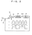
- FIG. 2 A conventional wri te circuit of the conventional magnetic card processing device is shown in Fig. 2 , wherein a signal “a” from the light receiver 23 of the rotary encoder 18 is processed by an encoder waveform processing circuit (encoder processor) 24 to form a pulse signal "b" of' a square wave which is applied to a write circuit 25 which generates an output signal "c" of writing data synchronized with the pulse signal "b" to be written into the magnetic stripe 17 by the magnetic head 16.
- encoder waveform processing circuit encoder processor
- the magnetic data reading circuit of the magnetic card processing device being an embodiment of the invention is shown in Fig. 3 .
- the signal “a” from the light receiver 23 of the rotary encoder 18 is converted to the pulse signal "b" of square waves by the encoder waveform processing circuit 24 to be outputted to a CPU (central processing unit) 26.
- a signal read by the magnetic head 16 is amplified by an amplifier 27 to generate an amplified signal “d” which is differentiated by a differentiator 28 to detect its peaks.
- a signal “e” of the detected peaks is compared with a slice level by a comparator 29, and the read signal "f” is applied to the CPU 26.
- the magnetic head 16, the amplifier 27, the differentiator 28, and the comparator 29 provide a read circuit means of this device.
- a distance (data length) p corresponding to data "O" of' the read signal "f"' is computed out by the lapse time tc1 and tc2 of rise and fall of signals before and after the data and lapse time tdl, td2, td3 and td4 of the pulse signal "b" before and after each time based on the equation (1) below;
- P AX td ⁇ 2 - tc ⁇ 1 / ( td ⁇ 2 - td ⁇ 1 ) + A + AX ( tc ⁇ 2 - td ⁇ 3 ) / ( td ⁇ 4 - td ⁇ 3 )
- a time length of the read signal corresponding to data "0" and “1” may be converted to a distance.
- This is a conveyance monitoring method, wherein data of "0” and “1” is judged after such conversion to the distance, thereby reading data even if the conveyance speed is changed .
- the magnetic card 10 is conveyed by same distance A, and the average speeds of A/T1 an A/T2 are different, whereby the distance by the time "t', of the average speed of A/T1 is different from the distance by the time "t" of' the average speed of A/T2, thereby causing an error in the distance.
- a read circuit neans for correcting the phase into complete 90° by differential, in which an output reduction portion "y" appears in processed waveforms of a signal " j " of Fig. which is a exact differentiated output, thereby providing a status that a low output card seems to be accessed.
- the output decrease portion "y" becomes Large one pulse may be regarded as two pulses in the succeeding step, viz. the comparator 29, resulting in wrong reading.
- an aim of the invention to provide a magnetic media processing device capable of precisely reading the read data without errors of distance conversion in spite of any rapid speed variation between several bits in a pulse output of an encoder for conveyance monitoring when read data is converted into a distance.
- a magnetic card processing device including an encoder for producing an output for a predetermined distance in a conveyance distance of a magnetic card on conveyance, a read circuit means for reading magnetic data stored in the magnetic card in synchronizing the output from the encoder to be processed as to its waveforms to produce read data, and an arithmetic means for converting a data length to data of a distance based on a time component of a data length of the read data of the read circuit means by employing the output signal from the encoder to read data based on distance data, wherein the arithmetic means is arranged to compensate the process delay time in a time component of read data produced from the read circuit means when the arithmetic means converts the data length into the data of distance.
- the process delay time by the read circuit means in the time component of the data length is compensated, viz. , subtracted, to be compensated to time of' the data length when any process delay does not happen, whereby distance conversion is executed by exact differential .
- distance conversion about the read data may be executed wi th a high accuracy without generating any errors.
- a magnetic media processing device employs the known magnetic card processing device transport arrangement (card reader) of Fig. 1 , a write circuit having the construction of Fig. 2 , and a read circuit means having the construction of Fig . 3 .
- the magnetic data reading circuit of the magnetic card processing device is shown in Fig. 3 .
- the signal “a” from the light receiver 23 of the rotary encoder 18 is converted to the pulse signal "b" of square waves by the encoder waveform processing circuit 24 to be outputted to a CPU (central processing unit) 26.
- a signal read by the magnetic head 16 is amplified by an amplifier 27 to generate an amplified signal “d” which is differentiated by a differentiator 28 to detect its peaks.
- a signal “e” of the detected peaks is compared with a slice level by a comparator 29, and the read signal "f” is applied to the CPU 26.
- the magnetic head 16, the amplifier 27, the differentiator 28, and the comparator 29 provide a read circuit means of this device.
- a distance (data length) p corresponding to data "O" of' the read signal "f"' is computed out by the lapse time tcl and tc2 of rise and fall of signals before and after the data and lapse time tdl, td2, td3 and td4 of the pulse signal "b" before and after each time based on the equation (1) below;
- P AX td ⁇ 2 - tc ⁇ 1 / ( td ⁇ 2 - td ⁇ 1 ) + A + AX ( tc ⁇ 2 - td ⁇ 3 ) / ( td ⁇ 4 - td ⁇ 3 )
- a time length of the read signal corresponding to data "0" and “1” may be converted to a distance.
- This is a conveyance monitoring method, wherein data of "0” and “1” is judged after such conversion to the distance, thereby reading data even if the conveyance speed is changed .
- the magnetic card 10 is conveyed by same distance A, and the average speeds of A/T1 an A/T2 are different, whereby the distance by the time "t', of the average speed of A/T1 is different from the distance by the time "t" of' the average speed of A/T2, thereby causing an error in the distance.
- a read circuit means for correcting the phase into complete 90° by differential, in which an output reduction portion "y" appears in processed waveforms of a signal " j " of Fig. 5 which is a exact differentiated output, thereby providing a status that a low output card seems to be accessed.
- the output decrease portion "y" becomes large , one pulse may be regarded as two pulses in the succeeding step, viz. the comparator 29, resulting in wrong reading.
- an arithmetic operation for converting a data length of read data into data of a distance based on a time component of the data length in the CPU 26 is executed by compensating a waveform process delay time "ta" in the time component of the read data produced from a read circuit means employing the magnetic head 16, the amplifier 27, the differentiator 28, and the comparator 29.
- the waveform process delay time "ta” may be measured in advance, and the measured value defines the time "ta".
- the CPU 26 time-shifts the signal f from the comparator 29 (which corresponds to the signal e from the differentiator at 28) by the delay time "ta" prior to comparison with the signal b from the encoder processor 24. From Fig. 4 , it can been that this can be done by delaying the signals "b” by the time “ta” since this is equivalent to a backward shift of signal "e” by the same time. If that backward shift occurred the reading edges of the pulses of signal "e” would coincide with the peaks and troughs of the signal "d”. Thus, if there was then a speed change at point "X", the delay time "ta” would not then appear as an error in the distant measurement. Instead, as shown by equation 2, signals are processed as if the delay time did not exist and thus a more accurate result is obtained.
- the rotary encoder 18 serves as an encoder, and a read circuit means is represented by the magnetic head 16, the amplifier 27, the differentiator 28 and the comparator 29.
- the arithmetic means is represented by the CPU 26.
Landscapes
- Engineering & Computer Science (AREA)
- Artificial Intelligence (AREA)
- Computer Vision & Pattern Recognition (AREA)
- Physics & Mathematics (AREA)
- General Physics & Mathematics (AREA)
- Theoretical Computer Science (AREA)
- Signal Processing For Digital Recording And Reproducing (AREA)
- Manufacturing Of Magnetic Record Carriers (AREA)
- Magnetic Heads (AREA)
- Devices For Checking Fares Or Tickets At Control Points (AREA)
Abstract
Description
- This invention relates to a magnetic media processing device for reading magnetic data magnetically recorded on a magnetic media such as a magnetic card to be processed thereby.
- A conventional magnetic card processing device is provided with a function for reading and writing magnetic data on a magnetic card employs a conveyance monitoring method for performing the reading-and-writing process with a high accuracy even though the conveyance speed of the magnetic card varies.
- The arrangement for transporting the magnetic card in such a magnetic card processing device is shown in
Fig. 1 . This arrangement is disclosed inEP-A-0613100 . Upper and lower pair ofrollers magnetic card 10 are arranged in a direction of conveyance, and rotated in a predetermined conveyance direction bypulleys 13 fixed on ends of shuts of the rollers which are driven by amotor 14 through a worm, a worm wheel and abelt 15. Themotor 14 is controlled to drive theconveyance rollers magnetic card 10 in a predetermined direction. - A
magnetic head 16 for executing a magnetic process of reading and writing magnetic data is disposed in a middle position of the pair ofconveyance rollers 11 to correspond to amagnetic stripe 17 of themagnetic card 10. - Beside the
head 16 there are disposed adetection roller 19 of arotary encoder 18 and themagnetic head 16 on the same line in a width direction of the conveyance direction. Thedetection roller 19 is pushed by apusher roller 20 to catch the conveyedmagnetic card 10, whereby theroller 19 is rotated by the conveyance of themagnetic card 10. - The
detection roller 19 is connected with aslit disc 21 having slits formed on a circumference thereof at predetermined equal intervals each of' which is detected by alight projector 22 and alight receiver 23, whereby a pulse signal is generated for each predetermined distance corresponding to a conveyance travel of themagnetic card 10. - A conventional wri te circuit of the conventional magnetic card processing device is shown in
Fig. 2 , wherein a signal "a" from thelight receiver 23 of therotary encoder 18 is processed by an encoder waveform processing circuit (encoder processor) 24 to form a pulse signal "b" of' a square wave which is applied to awrite circuit 25 which generates an output signal "c" of writing data synchronized with the pulse signal "b" to be written into themagnetic stripe 17 by themagnetic head 16. - In particular the magnetic data reading circuit of the magnetic card processing device being an embodiment of the invention is shown in
Fig. 3 . The signal "a" from thelight receiver 23 of therotary encoder 18 is converted to the pulse signal "b" of square waves by the encoderwaveform processing circuit 24 to be outputted to a CPU (central processing unit) 26. A signal read by themagnetic head 16 is amplified by anamplifier 27 to generate an amplified signal "d" which is differentiated by adifferentiator 28 to detect its peaks. A signal "e" of the detected peaks is compared with a slice level by acomparator 29, and the read signal "f" is applied to theCPU 26. Themagnetic head 16, theamplifier 27, thedifferentiator 28, and thecomparator 29 provide a read circuit means of this device. - In the
CPU 26 the time lapse of each time "tc" of rise and fall of the read signal "f'" is timed to be stored, the lapse of time "td" of rise of the pulse signal "b" from therotary encoder 18 is timed to be stored, and the movement travel A of themagnetic card 10 between pulses of the pulse signal "b" is previously obtained and known, whereby data of distance is made from time components of the data lengths. - In
Fig. 3 , for instance, a distance (data length) p corresponding to data "O" of' the read signal "f"' is computed out by the lapse time tc1 and tc2 of rise and fall of signals before and after the data and lapse time tdl, td2, td3 and td4 of the pulse signal "b" before and after each time based on the equation (1) below;
- According to this equation, a time length of the read signal corresponding to data "0" and "1" may be converted to a distance. This is a conveyance monitoring method, wherein data of "0" and "1" is judged after such conversion to the distance, thereby reading data even if the conveyance speed is changed .
- When a proper circuit for improving a reading ability about a low output card is installed into the read circuit means (16, 27, 28 and 29), particularly the
differential circuit 28, a processing delay of waveforms happens on reading. - As a rapid speed change happens between several bits of the pulse signal "b" based on deformation of the card or dirt adhered to the same , an error of the above-described distance conversion becomes enlarged, resulting at worst in a reading error.
- In
Fig. 4 , for instance, as a speed change happens in themagnetic card 10 at a point "X", a time length T2 of the pulse signal "b" of therotary encoder 18 is expressed by the following equation;
- Accordingly, when the read signal "f"' before and after of the point "X" is converted into distance, the time length Tl of the pulse signal "b" in the distance P1 is represented by the following equation ;

- Since an elapse time tcl of' the rise of the read signal "f"' is located in the time length T1, the above described distance P1 is computed out by these elapse data according to the above-mentioned equation (1) .
- During the time lengths T1 and T2 of the pulse signal "b" of the
rotary encoder 18, themagnetic card 10 is conveyed by same distance A, and the average speeds of A/T1 an A/T2 are different, whereby the distance by the time "t', of the average speed of A/T1 is different from the distance by the time "t" of' the average speed of A/T2, thereby causing an error in the distance. - When the peaks of the signal "d" , viz. , the peaks of the signal "d" produced from the
amplifier 27 are converted into a distance inFig. 4 , the error may be absorbed because i t is small. As described above, however, a process delay time "ta" for processing waveforms exists in thedifferentiator 28, and is regarded as time for conveying themagnetic card 10 whereby error of the above-mentioned distance is enlarged. - For instance, in
Fig. 4 , when the distance conversion is executed by peaks of the signal "d" , the error is so small that the distance P1 and P2 are converted as distances corresponding to two pulses (line "g") . When the distance conversion is executed by the read signal "f"' , the above-mentioned process delay time "ta" is treated as the time for conveying themagnetic card 10, whereby the error of the distance is enlarged. The distance P1 is converted as a distance for 1.8 pulses (line "h") and the distance P2 is converted as a distance for 2.2 pulses, so that error of the distance conversion is large resulting into reading error at worst. - To avoid the process delay of waveforms of the
differentiator 28, there may be proposed a read circuit neans for correcting the phase into complete 90° by differential, in which an output reduction portion "y" appears in processed waveforms of a signal " j " of Fig. which is a exact differentiated output, thereby providing a status that a low output card seems to be accessed. When the output decrease portion "y" becomes Large , one pulse may be regarded as two pulses in the succeeding step, viz. thecomparator 29, resulting in wrong reading. - As a result, when the waveform process delay by the read circuit means is tried to be resolved by a circuit, the reading function is lowered and such resolution cannot be performed by the circuit.
- It is, therefore, an aim of the invention to provide a magnetic media processing device capable of precisely reading the read data without errors of distance conversion in spite of any rapid speed variation between several bits in a pulse output of an encoder for conveyance monitoring when read data is converted into a distance.
- According to this invention, there is provided a magnetic card processing device including an encoder for producing an output for a predetermined distance in a conveyance distance of a magnetic card on conveyance, a read circuit means for reading magnetic data stored in the magnetic card in synchronizing the output from the encoder to be processed as to its waveforms to produce read data, and an arithmetic means for converting a data length to data of a distance based on a time component of a data length of the read data of the read circuit means by employing the output signal from the encoder to read data based on distance data, wherein the arithmetic means is arranged to compensate the process delay time in a time component of read data produced from the read circuit means when the arithmetic means converts the data length into the data of distance.
- According to this invention, when the data length is converted into the data of distance from the time component of the data length of the read data, the process delay time by the read circuit means in the time component of the data length is compensated, viz. , subtracted, to be compensated to time of' the data length when any process delay does not happen, whereby distance conversion is executed by exact differential . Thus, even if any speed variation happens between several bits in the pulse output of the encoder, distance conversion about the read data may be executed wi th a high accuracy without generating any errors.
- An embodiment of the invention will now be described with reference to the accompanying drawings, in which:
-
Fig. 1 is a perspective view of a known transport arrangement of a magnetic card processing device and has already been described; -
Fig. 2 shows signal waveforms of a write circuit in the arrangement ofFig. 1 and has already been described; -
Fig. 3 is a block diagram of a read circuit and signal waveforms in the arrangement ofFig 1 ; -
Fig. 4 shows signal waveforms illustrating a waveform process delay time in the arrangement ofFig 1 ; -
Fig. 5 shows signal waveforms by exact differential in the arrangement ofFig 1 ; and -
Fig. 6 shows signal waveforms for illustrating compensation against the waveform process delay as used in an embodiment of the invention. - A magnetic media processing device according to a preferred embodiment of this invention employs the known magnetic card processing device transport arrangement (card reader) of
Fig. 1 , a write circuit having the construction ofFig. 2 , and a read circuit means having the construction ofFig . 3 . - In particular the magnetic data reading circuit of the magnetic card processing device is shown in
Fig. 3 . The signal "a" from thelight receiver 23 of therotary encoder 18 is converted to the pulse signal "b" of square waves by the encoderwaveform processing circuit 24 to be outputted to a CPU (central processing unit) 26. A signal read by themagnetic head 16 is amplified by anamplifier 27 to generate an amplified signal "d" which is differentiated by adifferentiator 28 to detect its peaks. A signal "e" of the detected peaks is compared with a slice level by acomparator 29, and the read signal "f" is applied to theCPU 26. Themagnetic head 16, theamplifier 27, thedifferentiator 28, and thecomparator 29 provide a read circuit means of this device.
In theCPU 26 the time lapse of each time "tc" of rise and fall of the read signal "f'" is timed to be stored, the lapse of time "td" of rise of the pulse signal "b" from therotary encoder 18 is timed to be stored, and the movement travel A of themagnetic card 10 between pulses of the pulse signal "b" is previously obtained and known, whereby data of distance is made from time components of the data lengths. InFig. 3 , for instance, a distance (data length) p corresponding to data "O" of' the read signal "f"' is computed out by the lapse time tcl and tc2 of rise and fall of signals before and after the data and lapse time tdl, td2, td3 and td4 of the pulse signal "b" before and after each time based on the equation (1) below;
- According to this equation, a time length of the read signal corresponding to data "0" and "1" may be converted to a distance. This is a conveyance monitoring method, wherein data of "0" and "1" is judged after such conversion to the distance, thereby reading data even if the conveyance speed is changed .
- When a proper circuit for improving a reading ability about a low output card is installed into the read circuit means (16, 27, 28 and 29), particularly the
differential circuit 28, a processing delay of waveforms happens on reading. - As a rapid speed change happens between several bits of the pulse signal "b" based on deformation of the card or dirt adhered to the same , an error of the above-described distance conversion becomes enlarged, resulting at worst in a reading error.
- In
Fig. 4 , for instance, as a speed change happens in themagnetic card 10 at a point "X", a time length T2 of the pulse signal "b" of therotary encoder 18 is expressed by the following equation;
- Accordingly, when the read signal "f"' before and after of the point "X" is converted into distance, the time length Tl of the pulse signal "b" in the distance P1 is represented by the following equation ;

- Since an elapse time tcl of' the rise of the read signal "f"' is located in the time length T1, the above described distance P1 is computed out by these elapse data according to the above-mentioned equation (1) .
- During the time lengths Tl and T2 of the pulse signal "b" of the
rotary encoder 18, themagnetic card 10 is conveyed by same distance A, and the average speeds of A/T1 an A/T2 are different, whereby the distance by the time "t', of the average speed of A/T1 is different from the distance by the time "t" of' the average speed of A/T2, thereby causing an error in the distance. - When the peaks of the signal "d" , viz. , the peaks of the signal "d" produced from the
amplifier 27 are converted into a distance inFig. 4 , the error may be absorbed because i t is small. As described above, however, a process delay time "ta" for processing waveforms exists in thedifferentiator 28, and is regarded as time for conveying themagnetic card 10 whereby error of the above-mentioned distance is enlarged. - For instance, in
Fig. 4 , when the distance conversion is executed by peaks of the signal "d" , the error is so small that the distance P1 and P2 are converted as distances corresponding to two pulses (line "g") . When the distance conversion is executed by the read signal "f"' , the above-mentioned process delay time "ta" is treated as the time for conveying themagnetic card 10, whereby the error of the distance is enlarged. The distance P1 is converted as a distance for 1.8 pulses (line "h") and the distance P2 is converted as a distance for 2.2 pulses, so that error of the distance conversion is large resulting into reading error at worst. - To avoid the process delay of waveforms of the
differentiator 28, there may be proposed a read circuit means for correcting the phase into complete 90° by differential, in which an output reduction portion "y" appears in processed waveforms of a signal " j " ofFig. 5 which is a exact differentiated output, thereby providing a status that a low output card seems to be accessed. When the output decrease portion "y" becomes large , one pulse may be regarded as two pulses in the succeeding step, viz. thecomparator 29, resulting in wrong reading. - Therefore an arithmetic operation for converting a data length of read data into data of a distance based on a time component of the data length in the
CPU 26 is executed by compensating a waveform process delay time "ta" in the time component of the read data produced from a read circuit means employing themagnetic head 16, theamplifier 27, thedifferentiator 28, and thecomparator 29. The waveform process delay time "ta" may be measured in advance, and the measured value defines the time "ta". - The time "ta" is converted into time data converted by clock of the
CPU 26, and subtracts all of time data of a read signal "f"' for shift. That is, inFig. 6 , the distance for the data length "P" is obtained by employing the rise and fall elapse time tc1 and tc2 before and after the data length, the elapse time td1, td2, td3 and td4 of the pulse signal "b" before and after the respective time tc1 and tc2, a waveform process delay time "ta" , and a predetermined distance "A" converted into distances from distances of' the pulse signal "b" according to the equation below;
- Thus, in this embodiment of the present invention, the
CPU 26 time-shifts the signal f from the comparator 29 (which corresponds to the signal e from the differentiator at 28) by the delay time "ta" prior to comparison with the signal b from theencoder processor 24. FromFig. 4 , it can been that this can be done by delaying the signals "b" by the time "ta" since this is equivalent to a backward shift of signal "e" by the same time. If that backward shift occurred the reading edges of the pulses of signal "e" would coincide with the peaks and troughs of the signal "d". Thus, if there was then a speed change at point "X", the delay time "ta" would not then appear as an error in the distant measurement. Instead, as shown byequation 2, signals are processed as if the delay time did not exist and thus a more accurate result is obtained. - Therefore, even if any rapid speed change happens between several bits in pulse output "b" of the
rotary encoder 18, any error does not appear in the distance conversion, and precise distance conversion of' the read data may be performed. As a result, enough margin against read error may be ensured, and read function is improved. - In this embodiment, the
rotary encoder 18 serves as an encoder, and a read circuit means is represented by themagnetic head 16, theamplifier 27, thedifferentiator 28 and thecomparator 29. The arithmetic means is represented by theCPU 26.
Claims (3)
- A magnetic card processing device comprising:an encoder (18) for producing an output for a predetermined distance in a conveyance distance of a magnetic card (10) on conveyance,read circuit means (16, 27, 28 and 29) for reading magnetic data stored in said magnetic card (10) in synchronizing the output from said encoder (18) to be processed as to its waveforms to produce read data, and arithmetic means (26) for converting a data length to data of a distance based on a time component of a data length of the read data of said read circuit means (16, 27, 28 and 29) by employing the output signal from said encoder (18) to read data based on distance data,characterised in that :said arithmetic means (26) is arranged to compensate the process delay time in a time component of read data produced from said read circuit means (16, 27, 28 and 28) when said arithmetic means (26) converts the data length into the data of distance.
- A processing device according to claim 1, wherein the arithmetic means is arranged to compensate for the delay time by determining the delay time and time-shifting the read data relative to the encoder output by said delay time.
- A processing device according to claim 1 or claim 2, wherein said read circuit means includes a differentiator (28) to determine the changes in gradient of the read magnetic data, thereby to generate said read data.
Applications Claiming Priority (2)
| Application Number | Priority Date | Filing Date | Title |
|---|---|---|---|
| JP23239199A JP3748178B2 (en) | 1999-08-19 | 1999-08-19 | Magnetic media processing device |
| JP23239199 | 1999-08-19 |
Publications (3)
| Publication Number | Publication Date |
|---|---|
| EP1077428A2 EP1077428A2 (en) | 2001-02-21 |
| EP1077428A3 EP1077428A3 (en) | 2002-09-11 |
| EP1077428B1 true EP1077428B1 (en) | 2008-12-03 |
Family
ID=16938518
Family Applications (1)
| Application Number | Title | Priority Date | Filing Date |
|---|---|---|---|
| EP00306962A Expired - Lifetime EP1077428B1 (en) | 1999-08-19 | 2000-08-15 | Magnetic media processing device |
Country Status (5)
| Country | Link |
|---|---|
| US (1) | US6400517B1 (en) |
| EP (1) | EP1077428B1 (en) |
| JP (1) | JP3748178B2 (en) |
| AT (1) | ATE416433T1 (en) |
| DE (1) | DE60040953D1 (en) |
Families Citing this family (63)
| Publication number | Priority date | Publication date | Assignee | Title |
|---|---|---|---|---|
| US9305314B2 (en) | 2002-02-05 | 2016-04-05 | Square, Inc. | Methods of transmitting information to mobile devices using cost effective card readers |
| US9224142B2 (en) | 2002-02-05 | 2015-12-29 | Square, Inc. | Card reader with power efficient architecture that includes a power supply and a wake up circuit |
| US9262777B2 (en) * | 2002-02-05 | 2016-02-16 | Square, Inc. | Card reader with power efficient architecture that includes a wake-up circuit |
| US20120126010A1 (en) * | 2002-02-05 | 2012-05-24 | Amish Babu | Cost effective card reader configured to be coupled to a mobile device |
| US8235287B2 (en) | 2010-10-13 | 2012-08-07 | Square, Inc. | Read head device with slot configured to reduce torque |
| US9016572B2 (en) | 2010-10-13 | 2015-04-28 | Square, Inc. | Systems and methods for financial transaction through miniaturized card with ASIC |
| US8573486B2 (en) | 2010-10-13 | 2013-11-05 | Square, Inc. | Systems and methods for financial transaction through miniaturized card reader with confirmation of payment sent to buyer |
| US20120126006A1 (en) * | 2002-02-05 | 2012-05-24 | Jack Dorsey | Card reader with efficient encryption |
| US9495676B2 (en) | 2002-02-05 | 2016-11-15 | Square, Inc. | Method of transmitting information from a power efficient card to a mobile device |
| US8870071B2 (en) | 2010-10-13 | 2014-10-28 | Square, Inc. | Read head device with selected sampling rate |
| US9262757B2 (en) | 2002-02-05 | 2016-02-16 | Square, Inc. | Method of transmitting information from a card reader with a power supply and wake-up circuit to a mobile device |
| US9495675B2 (en) | 2002-02-05 | 2016-11-15 | Square, Inc. | Small card reader configured to be coupled to a mobile device |
| US20120005039A1 (en) | 2002-02-05 | 2012-01-05 | Jack Dorsey | Method of conducting financial transactions |
| US9582795B2 (en) | 2002-02-05 | 2017-02-28 | Square, Inc. | Methods of transmitting information from efficient encryption card readers to mobile devices |
| US9916581B2 (en) | 2002-02-05 | 2018-03-13 | Square, Inc. | Back end of payment system associated with financial transactions using card readers coupled to mobile devices |
| US20120126007A1 (en) * | 2002-02-05 | 2012-05-24 | Kartik Lamba | Card reader with communication protocol |
| US8876003B2 (en) | 2010-10-13 | 2014-11-04 | Square, Inc. | Read head device with selected output jack characteristics |
| US8500018B2 (en) | 2010-10-13 | 2013-08-06 | Square, Inc. | Systems and methods for financial transaction through miniaturized card reader with decoding on a seller's mobile device |
| US9324100B2 (en) | 2002-02-05 | 2016-04-26 | Square, Inc. | Card reader with asymmetric spring |
| US9286635B2 (en) | 2002-02-05 | 2016-03-15 | Square, Inc. | Method of transmitting information from efficient communication protocol card readers to mobile devices |
| JP4797136B2 (en) * | 2005-09-27 | 2011-10-19 | 日本電産サンキョー株式会社 | Magnetic data reading circuit and card processing apparatus |
| US9436955B2 (en) | 2009-06-10 | 2016-09-06 | Square, Inc. | Methods for transferring funds using a payment service where financial account information is only entered once with a payment service and need not be re-entered for future transfers |
| US8612352B2 (en) | 2010-10-13 | 2013-12-17 | Square, Inc. | Decoding systems with a decoding engine running on a mobile device and coupled to a payment system that includes identifying information of second parties qualified to conduct business with the payment system |
| CN102598046A (en) | 2009-10-13 | 2012-07-18 | 平方股份有限公司 | System and method for conducting financial transactions through a miniaturized card reader |
| US8571989B2 (en) | 2010-10-13 | 2013-10-29 | Square, Inc. | Decoding systems with a decoding engine running on a mobile device and coupled to a social network |
| US8678277B2 (en) | 2010-10-13 | 2014-03-25 | Square, Inc. | Decoding system coupled to a payment system that includes a cryptographic key |
| US8701996B2 (en) | 2010-10-13 | 2014-04-22 | Square, Inc. | Cost effective card reader and methods to be configured to be coupled to a mobile device |
| US8602305B2 (en) | 2010-10-13 | 2013-12-10 | Square, Inc. | Decoding systems with a decoding engine running on a mobile device configured to be coupled and decoupled to a card reader with wake-up electronics |
| US8640953B2 (en) | 2010-10-13 | 2014-02-04 | Square, Inc. | Decoding system running on a mobile device and coupled to a payment system that includes at least one of, a user database, a product database and a transaction database |
| US9619797B2 (en) | 2010-10-13 | 2017-04-11 | Square, Inc. | Payment methods with a payment service and tabs selected by a first party and opened by a second party at an geographic location of the first party's mobile device |
| US8573489B2 (en) | 2010-10-13 | 2013-11-05 | Square, Inc. | Decoding systems with a decoding engine running on a mobile device with a touch screen |
| US9454866B2 (en) | 2010-10-13 | 2016-09-27 | Square, Inc. | Method of conducting financial transactions where a payer's financial account information is entered only once with a payment system |
| US9576159B1 (en) | 2011-01-24 | 2017-02-21 | Square, Inc. | Multiple payment card reader system |
| DE202012100620U1 (en) | 2011-11-22 | 2012-06-13 | Square, Inc. | System for processing cardless payment transactions |
| US9741045B1 (en) | 2012-03-16 | 2017-08-22 | Square, Inc. | Ranking of merchants for cardless payment transactions |
| US11449854B1 (en) | 2012-10-29 | 2022-09-20 | Block, Inc. | Establishing consent for cardless transactions using short-range transmission |
| US9652791B1 (en) | 2013-02-08 | 2017-05-16 | Square, Inc. | Updating merchant location for cardless payment transactions |
| US9940616B1 (en) | 2013-03-14 | 2018-04-10 | Square, Inc. | Verifying proximity during payment transactions |
| CN103335671B (en) * | 2013-06-28 | 2015-06-10 | 中国科学院长春光学精密机械与物理研究所 | Absolute type grating scale absolute position information correction and read circuit |
| US9924322B2 (en) | 2013-07-23 | 2018-03-20 | Square, Inc. | Computing distances of devices |
| US10163148B1 (en) | 2013-11-13 | 2018-12-25 | Square, Inc. | Wireless beacon shopping experience |
| US8967465B1 (en) | 2013-11-27 | 2015-03-03 | Square, Inc. | Audio signaling training for bidirectional communications |
| US8910868B1 (en) | 2013-11-27 | 2014-12-16 | Square, Inc. | Firmware management |
| US8931699B1 (en) | 2013-12-11 | 2015-01-13 | Square, Inc. | Bidirectional audio communication in reader devices |
| US9633236B1 (en) | 2013-12-11 | 2017-04-25 | Square, Inc. | Power harvesting in reader devices |
| US10198731B1 (en) | 2014-02-18 | 2019-02-05 | Square, Inc. | Performing actions based on the location of mobile device during a card swipe |
| US9256769B1 (en) | 2014-02-25 | 2016-02-09 | Square, Inc. | Mobile reader device |
| US9569767B1 (en) | 2014-05-06 | 2017-02-14 | Square, Inc. | Fraud protection based on presence indication |
| US10026083B1 (en) | 2014-05-11 | 2018-07-17 | Square, Inc. | Tab for a venue |
| US10304043B1 (en) | 2014-05-21 | 2019-05-28 | Square, Inc. | Multi-peripheral host device |
| USD762651S1 (en) | 2014-06-06 | 2016-08-02 | Square, Inc. | Mobile device case |
| US9760740B1 (en) | 2014-06-23 | 2017-09-12 | Square, Inc. | Terminal case with integrated dual reader stack |
| US9256770B1 (en) | 2014-07-02 | 2016-02-09 | Square, Inc. | Terminal case with integrated reader and shortened base |
| US9799025B2 (en) | 2014-08-19 | 2017-10-24 | Square, Inc. | Energy harvesting bidirectional audio interface |
| US9355285B1 (en) | 2015-02-12 | 2016-05-31 | Square, Inc. | Tone-based wake up circuit for card reader |
| US9436938B1 (en) | 2015-05-13 | 2016-09-06 | Square, Inc. | Transaction payment processing by multiple data centers |
| US10628811B2 (en) | 2016-03-15 | 2020-04-21 | Square, Inc. | System-based detection of card sharing and fraud |
| US10410200B2 (en) | 2016-03-15 | 2019-09-10 | Square, Inc. | Cloud-based generation of receipts using transaction information |
| US10636019B1 (en) | 2016-03-31 | 2020-04-28 | Square, Inc. | Interactive gratuity platform |
| US10402807B1 (en) | 2017-02-28 | 2019-09-03 | Square, Inc. | Estimating interchange fees for card payments |
| US10410021B1 (en) | 2017-12-08 | 2019-09-10 | Square, Inc. | Transaction object reader with digital signal input/output and internal audio-based communication |
| US11087301B1 (en) | 2017-12-19 | 2021-08-10 | Square, Inc. | Tamper resistant device |
| USD905059S1 (en) | 2018-07-25 | 2020-12-15 | Square, Inc. | Card reader device |
Family Cites Families (3)
| Publication number | Priority date | Publication date | Assignee | Title |
|---|---|---|---|---|
| CH589895A5 (en) * | 1975-06-17 | 1977-07-29 | Landis & Gyr Ag | |
| US4264934A (en) * | 1979-04-23 | 1981-04-28 | Bell Telephone Laboratories, Incorporated | Rate adaptive writer for a card having a magnetizable surface |
| JPH06274703A (en) * | 1993-01-25 | 1994-09-30 | Omron Corp | Card processor |
-
1999
- 1999-08-19 JP JP23239199A patent/JP3748178B2/en not_active Expired - Fee Related
-
2000
- 2000-07-14 US US09/617,244 patent/US6400517B1/en not_active Expired - Lifetime
- 2000-08-15 DE DE60040953T patent/DE60040953D1/en not_active Expired - Lifetime
- 2000-08-15 EP EP00306962A patent/EP1077428B1/en not_active Expired - Lifetime
- 2000-08-15 AT AT00306962T patent/ATE416433T1/en not_active IP Right Cessation
Also Published As
| Publication number | Publication date |
|---|---|
| ATE416433T1 (en) | 2008-12-15 |
| JP3748178B2 (en) | 2006-02-22 |
| JP2001057025A (en) | 2001-02-27 |
| EP1077428A3 (en) | 2002-09-11 |
| DE60040953D1 (en) | 2009-01-15 |
| EP1077428A2 (en) | 2001-02-21 |
| US6400517B1 (en) | 2002-06-04 |
Similar Documents
| Publication | Publication Date | Title |
|---|---|---|
| EP1077428A2 (en) | Magnetic media processing device | |
| EP0430546A2 (en) | Color image recording apparatus | |
| US5077463A (en) | Bar code reading apparatus | |
| US5285328A (en) | Process for evaluating binary data of a magnetic storage card using curve patterns | |
| US3831009A (en) | Timing system for optically scanned documents | |
| US6010206A (en) | Method and system for detecting the position of a carriage | |
| US5712564A (en) | Magnetic ink recorder calibration apparatus and method | |
| US4774400A (en) | Method and apparatus for correcting angular deviation of optical recording medium | |
| JPH0528626A (en) | Card reader | |
| EP1058244A3 (en) | Apparatus for reading from or writing to optical recording media | |
| EP0807528B1 (en) | Method and system for detecting the position of a carriage | |
| US6976630B2 (en) | Bar-code reader, method of reading a bar code, and computer product | |
| US3959626A (en) | Distorted two frequency coded data interpreting method and apparatus | |
| JPH026124B2 (en) | ||
| JP3591167B2 (en) | Control method of magnetic ink character detection device | |
| JP2915727B2 (en) | Shading correction device such as image sensor | |
| JP2001344704A (en) | Magnetic medium reader | |
| JP5837328B2 (en) | Recording device | |
| JPS6136272B2 (en) | ||
| JP2580398B2 (en) | Printer print position correction processing method | |
| JP2003014425A (en) | Apparatus and method for detecting interval between wrapping portions of continuous wrapping body | |
| JP2006221511A (en) | Recording device and method for detecting conveyance jitter | |
| JPH0120792B2 (en) | ||
| EP0425705A1 (en) | Helical scan-type rotary head drum unit | |
| JPH09254480A (en) | Recording device |
Legal Events
| Date | Code | Title | Description |
|---|---|---|---|
| PUAI | Public reference made under article 153(3) epc to a published international application that has entered the european phase |
Free format text: ORIGINAL CODE: 0009012 |
|
| AK | Designated contracting states |
Kind code of ref document: A2 Designated state(s): AT BE CH CY DE DK ES FI FR GB GR IE IT LI LU MC NL PT SE |
|
| AX | Request for extension of the european patent |
Free format text: AL;LT;LV;MK;RO;SI |
|
| PUAL | Search report despatched |
Free format text: ORIGINAL CODE: 0009013 |
|
| AK | Designated contracting states |
Kind code of ref document: A3 Designated state(s): AT BE CH CY DE DK ES FI FR GB GR IE IT LI LU MC NL PT SE |
|
| AX | Request for extension of the european patent |
Free format text: AL;LT;LV;MK;RO;SI |
|
| RIC1 | Information provided on ipc code assigned before grant |
Free format text: 7G 06K 7/08 A, 7G 06K 7/016 B, 7G 06K 13/067 B |
|
| 17P | Request for examination filed |
Effective date: 20021105 |
|
| AKX | Designation fees paid |
Designated state(s): AT BE CH CY DE DK ES FI FR GB GR IE IT LI LU MC NL PT SE |
|
| RAP1 | Party data changed (applicant data changed or rights of an application transferred) |
Owner name: HITACHI-OMRON TERMINAL SOLUTIONS, CORP. |
|
| 17Q | First examination report despatched |
Effective date: 20070919 |
|
| GRAP | Despatch of communication of intention to grant a patent |
Free format text: ORIGINAL CODE: EPIDOSNIGR1 |
|
| GRAS | Grant fee paid |
Free format text: ORIGINAL CODE: EPIDOSNIGR3 |
|
| GRAA | (expected) grant |
Free format text: ORIGINAL CODE: 0009210 |
|
| AK | Designated contracting states |
Kind code of ref document: B1 Designated state(s): AT BE CH CY DE DK ES FI FR GB GR IE IT LI LU MC NL PT SE |
|
| REG | Reference to a national code |
Ref country code: GB Ref legal event code: FG4D |
|
| REG | Reference to a national code |
Ref country code: CH Ref legal event code: EP |
|
| REG | Reference to a national code |
Ref country code: IE Ref legal event code: FG4D |
|
| REF | Corresponds to: |
Ref document number: 60040953 Country of ref document: DE Date of ref document: 20090115 Kind code of ref document: P |
|
| PG25 | Lapsed in a contracting state [announced via postgrant information from national office to epo] |
Ref country code: ES Free format text: LAPSE BECAUSE OF FAILURE TO SUBMIT A TRANSLATION OF THE DESCRIPTION OR TO PAY THE FEE WITHIN THE PRESCRIBED TIME-LIMIT Effective date: 20090314 |
|
| NLV1 | Nl: lapsed or annulled due to failure to fulfill the requirements of art. 29p and 29m of the patents act | ||
| PG25 | Lapsed in a contracting state [announced via postgrant information from national office to epo] |
Ref country code: FI Free format text: LAPSE BECAUSE OF FAILURE TO SUBMIT A TRANSLATION OF THE DESCRIPTION OR TO PAY THE FEE WITHIN THE PRESCRIBED TIME-LIMIT Effective date: 20081203 Ref country code: NL Free format text: LAPSE BECAUSE OF FAILURE TO SUBMIT A TRANSLATION OF THE DESCRIPTION OR TO PAY THE FEE WITHIN THE PRESCRIBED TIME-LIMIT Effective date: 20081203 |
|
| PG25 | Lapsed in a contracting state [announced via postgrant information from national office to epo] |
Ref country code: BE Free format text: LAPSE BECAUSE OF FAILURE TO SUBMIT A TRANSLATION OF THE DESCRIPTION OR TO PAY THE FEE WITHIN THE PRESCRIBED TIME-LIMIT Effective date: 20081203 |
|
| PG25 | Lapsed in a contracting state [announced via postgrant information from national office to epo] |
Ref country code: PT Free format text: LAPSE BECAUSE OF FAILURE TO SUBMIT A TRANSLATION OF THE DESCRIPTION OR TO PAY THE FEE WITHIN THE PRESCRIBED TIME-LIMIT Effective date: 20090504 Ref country code: AT Free format text: LAPSE BECAUSE OF FAILURE TO SUBMIT A TRANSLATION OF THE DESCRIPTION OR TO PAY THE FEE WITHIN THE PRESCRIBED TIME-LIMIT Effective date: 20081203 Ref country code: SE Free format text: LAPSE BECAUSE OF FAILURE TO SUBMIT A TRANSLATION OF THE DESCRIPTION OR TO PAY THE FEE WITHIN THE PRESCRIBED TIME-LIMIT Effective date: 20090303 |
|
| PLBE | No opposition filed within time limit |
Free format text: ORIGINAL CODE: 0009261 |
|
| STAA | Information on the status of an ep patent application or granted ep patent |
Free format text: STATUS: NO OPPOSITION FILED WITHIN TIME LIMIT |
|
| PG25 | Lapsed in a contracting state [announced via postgrant information from national office to epo] |
Ref country code: DK Free format text: LAPSE BECAUSE OF FAILURE TO SUBMIT A TRANSLATION OF THE DESCRIPTION OR TO PAY THE FEE WITHIN THE PRESCRIBED TIME-LIMIT Effective date: 20081203 |
|
| 26N | No opposition filed |
Effective date: 20090904 |
|
| PG25 | Lapsed in a contracting state [announced via postgrant information from national office to epo] |
Ref country code: MC Free format text: LAPSE BECAUSE OF NON-PAYMENT OF DUE FEES Effective date: 20090831 |
|
| REG | Reference to a national code |
Ref country code: CH Ref legal event code: PL |
|
| PG25 | Lapsed in a contracting state [announced via postgrant information from national office to epo] |
Ref country code: LI Free format text: LAPSE BECAUSE OF NON-PAYMENT OF DUE FEES Effective date: 20090831 Ref country code: CH Free format text: LAPSE BECAUSE OF NON-PAYMENT OF DUE FEES Effective date: 20090831 |
|
| REG | Reference to a national code |
Ref country code: IE Ref legal event code: MM4A |
|
| PG25 | Lapsed in a contracting state [announced via postgrant information from national office to epo] |
Ref country code: IE Free format text: LAPSE BECAUSE OF NON-PAYMENT OF DUE FEES Effective date: 20090815 |
|
| PG25 | Lapsed in a contracting state [announced via postgrant information from national office to epo] |
Ref country code: GR Free format text: LAPSE BECAUSE OF FAILURE TO SUBMIT A TRANSLATION OF THE DESCRIPTION OR TO PAY THE FEE WITHIN THE PRESCRIBED TIME-LIMIT Effective date: 20090304 |
|
| PG25 | Lapsed in a contracting state [announced via postgrant information from national office to epo] |
Ref country code: IT Free format text: LAPSE BECAUSE OF FAILURE TO SUBMIT A TRANSLATION OF THE DESCRIPTION OR TO PAY THE FEE WITHIN THE PRESCRIBED TIME-LIMIT Effective date: 20081203 |
|
| PG25 | Lapsed in a contracting state [announced via postgrant information from national office to epo] |
Ref country code: LU Free format text: LAPSE BECAUSE OF NON-PAYMENT OF DUE FEES Effective date: 20090815 |
|
| PG25 | Lapsed in a contracting state [announced via postgrant information from national office to epo] |
Ref country code: CY Free format text: LAPSE BECAUSE OF FAILURE TO SUBMIT A TRANSLATION OF THE DESCRIPTION OR TO PAY THE FEE WITHIN THE PRESCRIBED TIME-LIMIT Effective date: 20081203 |
|
| PGFP | Annual fee paid to national office [announced via postgrant information from national office to epo] |
Ref country code: DE Payment date: 20130807 Year of fee payment: 14 |
|
| PGFP | Annual fee paid to national office [announced via postgrant information from national office to epo] |
Ref country code: GB Payment date: 20130814 Year of fee payment: 14 Ref country code: FR Payment date: 20130808 Year of fee payment: 14 |
|
| REG | Reference to a national code |
Ref country code: DE Ref legal event code: R119 Ref document number: 60040953 Country of ref document: DE |
|
| GBPC | Gb: european patent ceased through non-payment of renewal fee |
Effective date: 20140815 |
|
| REG | Reference to a national code |
Ref country code: DE Ref legal event code: R119 Ref document number: 60040953 Country of ref document: DE Effective date: 20150303 |
|
| REG | Reference to a national code |
Ref country code: FR Ref legal event code: ST Effective date: 20150430 |
|
| PG25 | Lapsed in a contracting state [announced via postgrant information from national office to epo] |
Ref country code: DE Free format text: LAPSE BECAUSE OF NON-PAYMENT OF DUE FEES Effective date: 20150303 Ref country code: GB Free format text: LAPSE BECAUSE OF NON-PAYMENT OF DUE FEES Effective date: 20140815 |
|
| PG25 | Lapsed in a contracting state [announced via postgrant information from national office to epo] |
Ref country code: FR Free format text: LAPSE BECAUSE OF NON-PAYMENT OF DUE FEES Effective date: 20140901 |