EP1074893A1 - Method and apparatus for image forming capable of effectively generating a consistent charge potential - Google Patents
Method and apparatus for image forming capable of effectively generating a consistent charge potential Download PDFInfo
- Publication number
- EP1074893A1 EP1074893A1 EP00116137A EP00116137A EP1074893A1 EP 1074893 A1 EP1074893 A1 EP 1074893A1 EP 00116137 A EP00116137 A EP 00116137A EP 00116137 A EP00116137 A EP 00116137A EP 1074893 A1 EP1074893 A1 EP 1074893A1
- Authority
- EP
- European Patent Office
- Prior art keywords
- charging
- gap
- voltage
- photoconductive member
- photoconductive
- Prior art date
- Legal status (The legal status is an assumption and is not a legal conclusion. Google has not performed a legal analysis and makes no representation as to the accuracy of the status listed.)
- Granted
Links
Images


Classifications
-
- G—PHYSICS
- G03—PHOTOGRAPHY; CINEMATOGRAPHY; ANALOGOUS TECHNIQUES USING WAVES OTHER THAN OPTICAL WAVES; ELECTROGRAPHY; HOLOGRAPHY
- G03G—ELECTROGRAPHY; ELECTROPHOTOGRAPHY; MAGNETOGRAPHY
- G03G15/00—Apparatus for electrographic processes using a charge pattern
- G03G15/02—Apparatus for electrographic processes using a charge pattern for laying down a uniform charge, e.g. for sensitising; Corona discharge devices
- G03G15/0208—Apparatus for electrographic processes using a charge pattern for laying down a uniform charge, e.g. for sensitising; Corona discharge devices by contact, friction or induction, e.g. liquid charging apparatus
-
- G—PHYSICS
- G03—PHOTOGRAPHY; CINEMATOGRAPHY; ANALOGOUS TECHNIQUES USING WAVES OTHER THAN OPTICAL WAVES; ELECTROGRAPHY; HOLOGRAPHY
- G03G—ELECTROGRAPHY; ELECTROPHOTOGRAPHY; MAGNETOGRAPHY
- G03G15/00—Apparatus for electrographic processes using a charge pattern
- G03G15/02—Apparatus for electrographic processes using a charge pattern for laying down a uniform charge, e.g. for sensitising; Corona discharge devices
-
- G—PHYSICS
- G03—PHOTOGRAPHY; CINEMATOGRAPHY; ANALOGOUS TECHNIQUES USING WAVES OTHER THAN OPTICAL WAVES; ELECTROGRAPHY; HOLOGRAPHY
- G03G—ELECTROGRAPHY; ELECTROPHOTOGRAPHY; MAGNETOGRAPHY
- G03G2215/00—Apparatus for electrophotographic processes
- G03G2215/02—Arrangements for laying down a uniform charge
- G03G2215/021—Arrangements for laying down a uniform charge by contact, friction or induction
Definitions
- the present invention relates to a method and apparatus for image forming, and more particularly to a method and apparatus for image forming that is capable of effectively generating a consistent charge potential.
- Charging the surface of a photoconductive member is one of basic and important processes performed in an image forming apparatus using an electrophotographic method, such as a copying machine, a facsimile machine, a printer, and so forth.
- electrophotographic method such as a copying machine, a facsimile machine, a printer, and so forth.
- various techniques for consistently charging the surface of the photoconductive member which are classified in two types.
- a charging member is configured to make its surface contacting the photoconductive member so as to provide charges evenly to the surface of the photoconductive member.
- a charging member is configured to be closely adjacent to the photoconductive member so as to provide a small gap between the charging member and the photoconductive member.
- the non-contact type charging has an advantage in the performance of a charging operation, particularly in evenly charging the surface of the photoconductive member.
- the non-contact type charging has a drawback of a production of ozone. Therefore, the contact type is now becoming a mainstream.
- the contact type charging also has several drawbacks due to its mechanism which causes the charging member such as a charging roller to directly contact the surface of the photoconductive member.
- the photoconductive member will be contaminated due to the contact with the charging roller so that an abnormal image will be produced.
- the photoconductive member may have a crack at a place in the surface contacting the charging roller if an excess contact pressure is loaded onto the surface of the photoconductive member.
- the charging roller itself may be contaminated by the toner deposited on the photoconductive member. If the limit of the contamination is violated, the charging roller reduces the charge performance, particularly the consistency of the charge.
- the surface of the photoconductive member may be worn by the contact of the charging roller and the charge potential is reduced.
- the photoconductive member has a pinhole, it has not a sufficient margin against a leakage of the charge through the pinhole.
- the charging roller is arranged to merely have an extreme small gap relative to the photoconductive member and to charge the photoconductive member from that distance.
- the charging roller is made of elastic material, it is difficult to make such a gap in an accurate manner, otherwise it brings a cost problem.
- a novel charging apparatus includes a charging member which is arranged to be adjacent to a photoconductive member with a gap having a tolerance in a charging region relative to the photoconductive member and is applied with a voltage including a direct current voltage under a constant voltage control including an alternating current element to apply a charge to the photoconductive member.
- the above-mentioned alternating current element has a peak-to-peak voltage at least twice as great as a charge-start voltage to be applied to the charging member at a maximum gap within a range of the gap having the tolerance.
- the charging member may be a rotatable elastic roller.
- the photoconductive member may be a rotatable photoconductive drum or belt.
- the tolerance of the gap may be caused by an inaccurate plainness of a surface of the charging member.
- the tolerance of the gap may be caused by inaccuracy of parallel of the charging member and the photoconductive member.
- the maximum gap may be greater than a maximum gap requiring a charge-start voltage greater than the charge-start voltage required in a case when the gap is substantially 0.
- the charging member may be arranged to be adjacent to and partly contact the photoconductive member so as to partly form the gap having the tolerance.
- the present invention further provides a novel charging method.
- the novel charging method includes the steps of providing, superposing, and applying.
- the providing step provides a charging member to form a gap having a tolerance in a charging region relative to a photoconductive member.
- the superposing step superposes an alternating current element to a direct current voltage under a constant voltage control.
- the alternating current element has a peak-to-peak voltage at least twice as great as a charge-start voltage to be applied to the charging member at a maximum gap within a range of the gap having the tolerance.
- the applying step applies the direct current voltage with the superposed alternating current element to the charging member to apply a charge to the photoconductive member.
- a novel image forming apparatus includes a photoconductive member and a charging apparatus.
- the charging apparatus charges the photoconductive member and includes a charging member arranged to be adjacent to the photoconductive member to form a gap having a tolerance in a charging region relative to the photoconductive member.
- the charging member is applied with a direct current voltage under a constant voltage control including an alternating current element to apply a charge to the photoconductive member.
- the alternating current element has a peak-to-peak voltage at least twice as great as a charge-start voltage to be applied to the charging member at a maximum gap within a range of the gap having the tolerance.
- a novel charging apparatus includes a charging member which is arranged to be adjacent to a photoconductive member with a gap having a tolerance in a charging region relative to the photoconductive member and is applied with a voltage including a direct current voltage under a constant voltage control including an alternating current element under a constant current control to apply a charge to the photoconductive member.
- the alternating current element has a peak-to-peak voltage at least twice as great as a charge-start voltage to be applied to the charging member at a maximum gap within a range of the gap having the tolerance.
- the charging member may be a rotatable elastic roller.
- the photoconductive member may be a rotatable photoconductive drum or belt.
- the tolerance of the gap may be caused by an inaccurate plainness of a surface of the charging member.
- the tolerance of the gap may be caused by inaccuracy of parallel of the charging member and the photoconductive member.
- the maximum gap may be greater than a maximum gap requiring a charge-start voltage greater than the charge-start voltage required in a case when the gap is substantially 0.
- the charging member may be arranged to be adjacent to and partly contact the photoconductive member so as to partly form the gap having the tolerance.
- a novel charging method includes the steps of providing, superposing, and applying.
- the providing step provides a charging member to form a gap having a tolerance in a charging region relative to a photoconductive member.
- the superposing step superposes an alternating current element under a constant current control to a direct current voltage under a constant voltage control.
- the alternating current element has a peak-to-peak voltage at least twice as great as a charge-start voltage to be applied to the charging member at a maximum gap within a range of the gap having the tolerance.
- the applying step applies the direct current voltage with the superposed alternating current element to the charging member to apply a charge to the photoconductive member.
- a novel image forming apparatus includes a photoconductive member and a charging apparatus.
- the charging apparatus charges the photoconductive member and includes a charging member arranged to be adjacent to the photoconductive member to form a gap having a tolerance in a charging region relative to the photoconductive member.
- the charging member is applied with a direct current voltage under a constant voltage control including an alternating current element under a constant current control to apply a charge to the photoconductive member.
- the alternating current element has a peak-to-peak voltage at least twice as great as a charge-start voltage to be applied to the charging member at a maximum gap within a range of the gap having the tolerance.
- a novel charging apparatus includes a charging member which is arranged to be adjacent to a photoconductive member to form a gap having a tolerance in a charging region relative to the photoconductive member and is applied with a direct current voltage under a constant voltage control including an alternating current element to apply a charge to the photoconductive member.
- the gap has a mean value at each position in the charging region in longitudinal and circumference directions of the charging member is greater than 10 ⁇ m and of which deviation is greater than 10 ⁇ m relative to the mean value.
- the alternating current element has a peak-to-peak voltage at least twice as great as a charge-start voltage to be applied to the charging member at a maximum gap within a range of the gap having the tolerance.
- the charging member may be a rotatable elastic roller.
- the photoconductive member may be a rotatable photoconductive drum or belt.
- the gap may be formed with an intermediate member to be placed between the charging member and the photoconductive member and a thickness of the intermediate member determines the maximum gap.
- the charging member may be arranged to be adjacent to and partly contact the photoconductive member so as to partly form the gap having the tolerance.
- a novel charging method includes the step of providing and applying.
- the providing step provides a charging member to form a gap having a tolerance in a charging region relative to the photoconductive member.
- the gap has a mean value at each position in the charging region in longitudinal and circumference directions of the charging member is greater than 10 ⁇ m and a deviation of the predetermined gap relative to the mean value is greater than 10 ⁇ m.
- the applying step applies to the charging member a direct current voltage under a constant voltage control including an alternating current element to charge the photoconductive member.
- the alternating current element has a peak-to-peak voltage at least twice as great as a charge-start voltage to be applied to the charging member at a maximum gap within a range of the gap having the tolerance.
- a novel image forming apparatus includes a photoconductive member and a charging apparatus for charging the photoconductive member.
- the charging apparatus includes a charging member which is arranged to be adjacent to the photoconductive member to form a gap having a tolerance in a charging region relative to the photoconductive member and is applied with a direct current voltage under a constant voltage control and an alternating current element to apply a charge to the photoconductive member.
- the gap has a mean value at each position in the charging region in longitudinal and circumference directions of the charging member is greater than 10 ⁇ m and of which deviation is greater than 10 ⁇ m relative to the mean value.
- the alternating current element has a peak-to-peak voltage at least twice as great as a charge-start voltage to be applied to the charging member at a maximum gap within a range of the gap having the tolerance.
- a novel charging apparatus includes a charging member which is arranged to be adjacent to a photoconductive member to form a gap having a tolerance in a charging region relative to the photoconductive member and is applied with a direct current voltage under a constant voltage control including an alternating current element under a constant current control to apply a charge to the photoconductive member.
- the gap has a mean value at each position in the charging region in longitudinal and circumference directions of the charging member is greater than 10 ⁇ m and of which deviation is greater than 10 ⁇ m relative to the mean value.
- the charging member may be a rotatable elastic roller.
- the photoconductive member may be a rotatable photoconductive drum or belt.
- the charging member may have a volume resistance ratio of 105 ⁇ m or more.
- the charging member may be arranged to be adjacent to and partly contact the photoconductive member so as to partly form the gap having the tolerance.
- a novel charging method includes the steps of providing and applying.
- the providing step provides a charging member to form a gap having a tolerance in a charging region relative to the photoconductive member.
- the gap has a mean value at each position in the charging region in longitudinal and circumference directions of the charging member is greater than 10 ⁇ m and a deviation of the predetermined gap relative to the mean value is greater than 10 ⁇ m.
- the applying step applies to the charging member a direct current voltage under a constant voltage control including an alternating current element under a constant current control to apply a charge to the photoconductive member.
- the alternating current element has a peak-to-peak voltage at least twice as great as a charge-start voltage to be applied to the charging member at a maximum gap within a range of the gap having the tolerance.
- a novel image forming apparatus includes a photoconductive member and a charging apparatus.
- the charging apparatus charges the photoconductive member and includes a charging member which is arranged to be adjacent to the photoconductive member to form a gap having a tolerance in a charging region relative to the photoconductive member and is applied with a direct current voltage under a constant voltage control and an alternating current element under a constant current control to apply a charge to the photoconductive member.
- the gap has a mean value at each position in the charging region in longitudinal and circumference directions of the charging member is greater than 10 ⁇ m and of which deviation is greater than 10 ⁇ m relative to the mean value.
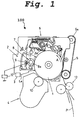
- FIG. 1 there is illustrated an image forming mechanism 100 according to an embodiment of the present invention.
- the image forming mechanism 100 of Fig. 1 is used in an image forming apparatus, i.e., a copying machine, a facsimile machine, or a printer.
- the image forming mechanism 100 includes a photoconductive drum 1 held in rotation in the direction indicated by an arrow A and of which surface is subjected to be evenly charged.
- the image forming mechanism 100 further includes a main charging unit 2, a light emitting unit 3, a development unit 4, a transfer belt 5, a cleaning unit 6, and a quenching lamp 7, which are arranged around the periphery of the photoconductive drum 1.
- the main charging unit 2 charges the surface of the photoconductive drum 1 and includes a charging roller 8, and a roller cleaning member 9.
- the charging roller 8 is arranged close to the photoconductive drum 1 so as to form a predetermined gap within a charging region relative to the photoconductive drum 1.
- the roller cleaning member 9 is made of rubber foam, for example, and is held in contact with the charging roller 8 so as to clean the surface of the charging roller 8.
- the charge roller 8 includes a metal core 11 to which a power supply unit 12 supplies DC (direct current) and AC (alternating current) biases both constant-voltage-controlled. These DC and AC biases may be constant-current-controlled. Thus, the main charging unit 2 evenly charges the surface of the photoconductive drum 1.
- the photoconductive drum 1 includes a aluminum-made base tube having multiple coating layers such as a UL (under layer), a CGL (carrier generation layer), and a CTL (carrier transport layer). This photoconductive drum 1 is driven at a constant velocity in the direction of the arrow A by a main motor (not shown).
- a main motor not shown.
- the charging roller 8 is held for rotation on both ends of the metal core 11.
- the charging roller 8 includes an elastic roller layer 8a over the metal core 11.
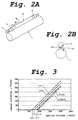
- a Teflon-coated tube 14 is tightly fixed, as shown in Fig. 2A.
- a gap 15 is formed in a development region 16 between the longitudinal surfaces of the elastic roller layer 8a and the photoconductive drum 1. Since the charging roller 8 and the photoconductive drum 1 generally have distortions on the plainness of the surface thereof in the longitudinal and circumference directions, indicated by arrows B and C, respectively, in Fig. 2A, the above-mentioned gap 15 (Fig.
- the thickness of the Teflon tube 14 determines the maximum gap.
- the gap 15 has a mean value of 10 ⁇ m or more and varies by 10 ⁇ m or more relative to the mean value.
- a voltage to be applied for the charging operation is defined based on the experimental result which is explained later. That is, in the image forming mechanism 100, a voltage that includes an alternative current element is applied to the development region 16 formed between the charging roller 8 and the photoconductive drum 1. This voltage has a peak-to-peak value which is twice or more as high as a voltage at which the area of the maximum gap is started to be charged.
- the above-mentioned alternative current element is controlled at a predetermined constant current value so that the voltage has an AC (alternating current) peak-to-peak value which is twice or more as high as a DC (direct current) voltage at which the area of the maximum gap is started to be charged, as mentioned above.
- This DC voltage is referred to as a charge-start voltage.
- the surface of the photoconductive drum 1 is evenly charged by the charging roller 8.
- the charged surface is exposed to light La corresponding to image information sent from the right emitting unit 3. Thereby, an electrostatic latent image is formed on the surface of the photoconductive drum 1.
- the electrostatic latent image is moved to a position close to the development unit 4 and is supplied with toner by a development sleeve 10 which is included in the development unit 4. Thereby, the latent image is visualized and is formed as a toner image on the photoconductive drum 1.
- a recording sheet P is transported from a sheet supply unit (not shown) and is stopped at registration rollers 13 which is included in the image forming mechanism 100.
- the registration roller 13 releases the recording sheet P when the leading edge of the recording sheet P is precisely synchronized with the leading edge of the toner image on the photoconductive drum 1. Therefore, the recording sheet P is transported to the transfer belt 5 which then transfers the toner image of the photoconductive drum 1 to the recording sheet P.
- the recording sheet P When the recording sheet P is further transported by the transfer belt 5 to a driving roller 5a of the transfer belt 5, the recording sheet P straightly advances but the surface of the driving roller 5a rotates, that is, moving away from the recording sheet P. Thereby, the recording sheet P is separated from the transfer belt 5. After that, the recording sheet P is transported to a fixing unit (not shown) which fixes the toner onto the recording sheet P with heat and pressure. The recording sheet P having the fixed toner image is then ejected to an ejection tray or the like.
- the toner remaining on the surface of the photoconductive drum 1 is collected by a cleaning blade 6a of the cleaning unit 6 and is returned to the development unit 4 so as to be reused.
- FIG. 3 shows relationships in two experiment cases between an application voltage to be applied to the charging roller 8 and a charging potential to be produced on the surface of the photoconductive drum 1 by the application voltage.
- the photoconductive drum 1 is rotated at a line velocity of 230 mm/s and the charging roller 8 is applied with a DC (direct current) bias having a constant DC voltage.
- the charging roller 8 is caused to contact the surface of the photoconductive drum 1 so as to perform the contact type charging operation.
- the charging roller 8 is caused to form a gap relative to the surface of the photoconductive drum 1 so as to perform the non-contact type charging operation.
- the photoconductive drum 1 is charged when it is applied with a voltage equal to or greater than a threshold value, or each charge-start voltage (i.e., -651 volts, -745 volts, -875 volts, or -916 volts), but is not charged when it is applied with a voltage smaller than each of the absolute values of the charge-start voltages.
- a threshold value or each charge-start voltage (i.e., -651 volts, -745 volts, -875 volts, or -916 volts)
- the potential of the surface of the photoconductive drum 1 will have a linear relationship having a gradient of approximately 1 relative to the applied voltage, regardless of the conditions if the charging roller 8 contacts the photoconductive drum 1 or not, as shown in Fig. 3.
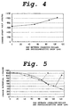
- Fig. 4 shows variations of the above-mentioned charge performance when the charging roller 8 is stepwise removed away from the photoconductive drum 1.
- the charging roller 8 uses the Teflon tubes 14, as illustrated in Fig. 2A, so as to have the gap 15, as illustrated in Fig. 2B, relative to the photoconductive drum 1. That is, the thickness of the Teflon tube 14 is regarded as the maximum gap.
- Teflon tube 14 different from each other in thickness (i.e., 53 ⁇ m, 87 ⁇ m, and 106 ⁇ m) were used in the experiment.
- the charge performance performed when the DC-constant-voltage bias was applied to the charging roller 8 was measured.
- the measurement result is plotted in the graph of Fig. 4 in which the measurement result from the above-described case when the gap 15 is 0, as shown in Fig. 3, is also plotted therein.
- the charge performance shown in Fig. 3 can lead to an observation in which the charge potential of the photoconductive drum 1 depends on the gap 15 formed between the charge roller 8 and the photoconductive drum 1 under the conditions that a predetermined DC voltage is applied to the charge roller 8. This observation is understood from the Paschen's discharge law.
- Fig. 5 shows both simulation and experiment results with respect to the relationship between the gap 15 and the charge performance.
- the simulation result is labeled with a letter A and the experiment result is labeled with a letter of B.
- the graph of Fig. 5 is in the case when the DC application voltage, or the DC bias, is fixed to -1600 volts.
- the results of the simulation and experiment shown in Fig. 5 are similar to each other.
- the gap 15 and the charge performance are in the relationship having a variation ratio of approximately 6 volts/ ⁇ m with the gap 15 greater than 20 ⁇ m when the charge roller 8 is applied with the voltage under the constant DC-voltage control.
- an image forming mechanism i.e., the image forming mechanism 100
- a charging roller i.e., the charging roller 8
- a photoconductive drum i.e., the photoconductive drum 1
- allowable variations of the charge potential is ⁇ 30 volts for in case of a mono-color image forming machine and ⁇ 10 volts for in case of a multi-color image forming machine.
- These allowable variations of the charge potential can be converted into variations of the gap 15.
- the allowable variations of the gap 15 is 10 ⁇ m in case of the mono-color image forming machine and 3.3 ⁇ m in case of the multi-color image forming machine.
- Both the charging roller 8 and the photoconductive drum 1 generally have distortions in the plainness of the surface thereof, particularly in their longitudinal direction, and in roughness, waves, and so forth. With consideration given to combinations of allowable tolerances for the above-mentioned distortions, it may greatly be difficult to achieve the above-mentioned extremely small variations of the gap 15.
- Fig. 6 shows a graph of the charge performance from an experiment performed using the applied voltage that includes a constant DC voltage with an AC constant voltage superposed on the constant DC voltage in the image forming mechanism 100 employing the non-contact type charging roller having a small gap relative to the photoconductive drum. From this graph of Fig. 6, it is understood that the photoconductive drum 1 can be charged with the charge potential approximately equal to the applied DC voltage (i.e., -700 volts) by applying the AC peak-to-peak voltage approximately twice as great as the charge-start voltage used during the application of the constant DC voltage (see Fig. 3) to the charging roller 8 in each of the cases where the gap 15 is 0 ⁇ m, 53 ⁇ m, 87 ⁇ m, and 106 ⁇ m.
- the applied DC voltage i.e., -700 volts
- Fig. 7 shows a result of an experimental in which the AC bias to be superposed on the constant DC voltage (i.e., the DC bias) is controlled to feed a constant current. From this graph of Fig. 7, it is understood that the relationship between the total current flowing through the AC bias and the charge potential charged on the surface of the photoconductive drum 1 can be made approximately constant, regardless of the gap 15, by a control of the AC bias superposed on the constant DC voltage to pass a constant current.
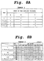
- Fig. 8A shows Table 1 which represents evaluation results relative to an output halftone image in each of the cases where the gap 15 is 0 ⁇ m, 53 ⁇ m, 87 ⁇ m, and 106 ⁇ m, having no gap deviation.
- Table 1 a preferable evaluation result is represented by a circle mark and a defective result is represented by a cross mark.
- the applied voltages A, B, and C represent the applications of the constant DC voltage, the constant DC voltage with the superposed constant AC voltage, and the constant DC voltage with the superposed constant AC current.
- the AC peak-to-peak voltage is twice or more as large as the charge-start voltage supplied at the maximum gap.
- the AC bias passes a current which generates a voltage twice or more as large as the charge-start voltage applied at the maximum gap.
- the output halftone image had defective white spots was evaluated as a defective image in the cases where the gap 15 was greater than 53 ⁇ m with the applied voltage A and in the cases where the gap 15 was 106 ⁇ m with the applied voltages B and C. From this, it is understood that superposing the AC bias on the application of the constant DC voltage has a preferable effect in case of the non-contact type charging method.
- Fig. 8B shows Table 2 representing evaluation results relative to an output halftone image in each of the different DC biases (i.e., -400 volts, -600 volts, and -800 bolts) with the AC bias varied.
- the gap 15 was provided with a deviation.
- the gap deviation of the gap 15 in the case I is such that the maximum gap was 53 ⁇ m at the left side and 0 at the right side.
- the maximum gap was 53 ⁇ m at the left side and 0 at the right side.
- the maximum gap was 106 ⁇ m at the left side and 0 at the right side.
- a preferable evaluation result is represented by a circle mark
- a defective result is represented by a cross mark.
- a dash mark represents a case of no judgement and a triangle mark represents a case in which an inconsistent image density was observed but it was allowable.
- the limit of the allowable gap deviation with the applied voltage A is about 10 ⁇ m which approximately proves the simulation result and the gap having the deviation greater than 10 ⁇ m causes the defective image. It is also understood that the halftone images with the applied voltages B and C were examined as superior image quality, except for the case of the gap deviation of 106 ⁇ m. When the gap deviation was about 106 ⁇ m in both the applied voltages B and C, the white spot phenomenon was observed. However, the appearance level of this phenomenon was almost equal to what it would be in the case having no gap deviation.
- the main charging unit 2 can avoid the problem of inconsistency of the image density to be caused due to the uneven main charging by applying the constant DC voltage superposed with the AC of which AC element has a peak-to-peak voltage twice or more as great as the charge-start voltage applied to the charging roller 8 at the maximum gap. Also, the main charging unit 2 can avoid the problem of inconsistency of the image density to be caused due to the uneven main charging by applying the constant DC voltage superposed with the AC of which AC element is controlled to have a current for producing a peak-to-peak voltage twice or more as great as the charge-start voltage applied to the charging roller 8 at the maximum gap.
- the photoconductive drum 1 can be prevented from contamination by toner of the charging roller 8 by the configuration in which the charging roller 8 contacts the photoconductive drum 1.
- the contact of the charging roller 8 to the photoconductive drum 1 further leads to avoidance of wearing of coating by contact, and so forth.
- the above-described main charging unit 2 applying the constant DC voltage superposed with the AC can sufficiently be employed in a main charging system having a mixture of the contact and non-contact techniques.
- the DC bias was set to -1300 volts and the development bias was set to -650 volts.
- the DC bias was set to - 600 volts and the AC bias was set to 2000 volts which was twice or more as great as the charge-start voltage applied to the charging roller 8 at the maximum gap of 106 ⁇ m.
- the DC bias was set to -600 volts and the AC bias was set to a current of 2.5 mA, equivalent to a frequency of 2 kHz, for producing an AC peak-to-peak voltage twice or more as great as the charge-start voltage applied to the charging roller 8 at the maximum gap.
- the charging roller is needed to have the volume resistance greater than 1x10 5 ⁇ m in the case where the mixture of the contact and non-contact charging methods is applied.
Landscapes
- Physics & Mathematics (AREA)
- Engineering & Computer Science (AREA)
- Plasma & Fusion (AREA)
- General Physics & Mathematics (AREA)
- Electrostatic Charge, Transfer And Separation In Electrography (AREA)
Abstract
Description
- This application claims priority to Japanese patent application Nos. JPAP11-218878 filed on August 2, 1999 and JPAP11-218885 filed on August 2, 1999 in the Japanese Patent Office, the entire contents of which are hereby incorporated by reference.
- The present invention relates to a method and apparatus for image forming, and more particularly to a method and apparatus for image forming that is capable of effectively generating a consistent charge potential.
- Charging the surface of a photoconductive member is one of basic and important processes performed in an image forming apparatus using an electrophotographic method, such as a copying machine, a facsimile machine, a printer, and so forth. There have developed various techniques for consistently charging the surface of the photoconductive member, which are classified in two types. In a first type which is referred to as a contact type charging technique, a charging member is configured to make its surface contacting the photoconductive member so as to provide charges evenly to the surface of the photoconductive member. In a second type which is referred to as a non-contact type charging technique, a charging member is configured to be closely adjacent to the photoconductive member so as to provide a small gap between the charging member and the photoconductive member.
- The non-contact type charging has an advantage in the performance of a charging operation, particularly in evenly charging the surface of the photoconductive member. However, the non-contact type charging has a drawback of a production of ozone. Therefore, the contact type is now becoming a mainstream.
- However, the contact type charging also has several drawbacks due to its mechanism which causes the charging member such as a charging roller to directly contact the surface of the photoconductive member. For example, the photoconductive member will be contaminated due to the contact with the charging roller so that an abnormal image will be produced. The photoconductive member may have a crack at a place in the surface contacting the charging roller if an excess contact pressure is loaded onto the surface of the photoconductive member.
- Further, the charging roller itself may be contaminated by the toner deposited on the photoconductive member. If the limit of the contamination is violated, the charging roller reduces the charge performance, particularly the consistency of the charge.
- Further, the surface of the photoconductive member may be worn by the contact of the charging roller and the charge potential is reduced.
- In addition, if the photoconductive member has a pinhole, it has not a sufficient margin against a leakage of the charge through the pinhole.
- In order to avoid these problems, the charging roller is arranged to merely have an extreme small gap relative to the photoconductive member and to charge the photoconductive member from that distance. However, if the charging roller is made of elastic material, it is difficult to make such a gap in an accurate manner, otherwise it brings a cost problem.
- The present invention provides a novel charging apparatus. In one example, a novel charging apparatus includes a charging member which is arranged to be adjacent to a photoconductive member with a gap having a tolerance in a charging region relative to the photoconductive member and is applied with a voltage including a direct current voltage under a constant voltage control including an alternating current element to apply a charge to the photoconductive member. The above-mentioned alternating current element has a peak-to-peak voltage at least twice as great as a charge-start voltage to be applied to the charging member at a maximum gap within a range of the gap having the tolerance.
- The charging member may be a rotatable elastic roller.
- The photoconductive member may be a rotatable photoconductive drum or belt.
- The tolerance of the gap may be caused by an inaccurate plainness of a surface of the charging member.
- The tolerance of the gap may be caused by inaccuracy of parallel of the charging member and the photoconductive member.
- The maximum gap may be greater than a maximum gap requiring a charge-start voltage greater than the charge-start voltage required in a case when the gap is substantially 0.
- The charging member may be arranged to be adjacent to and partly contact the photoconductive member so as to partly form the gap having the tolerance.
- The present invention further provides a novel charging method. In one example, the novel charging method includes the steps of providing, superposing, and applying. The providing step provides a charging member to form a gap having a tolerance in a charging region relative to a photoconductive member. The superposing step superposes an alternating current element to a direct current voltage under a constant voltage control. In this case, the alternating current element has a peak-to-peak voltage at least twice as great as a charge-start voltage to be applied to the charging member at a maximum gap within a range of the gap having the tolerance. The applying step applies the direct current voltage with the superposed alternating current element to the charging member to apply a charge to the photoconductive member.
- Further, the present invention provides an image forming apparatus. In one example, a novel image forming apparatus includes a photoconductive member and a charging apparatus. The charging apparatus charges the photoconductive member and includes a charging member arranged to be adjacent to the photoconductive member to form a gap having a tolerance in a charging region relative to the photoconductive member. The charging member is applied with a direct current voltage under a constant voltage control including an alternating current element to apply a charge to the photoconductive member. In this case, the alternating current element has a peak-to-peak voltage at least twice as great as a charge-start voltage to be applied to the charging member at a maximum gap within a range of the gap having the tolerance.
- Further, the present invention provides a charging apparatus. In one example, a novel charging apparatus includes a charging member which is arranged to be adjacent to a photoconductive member with a gap having a tolerance in a charging region relative to the photoconductive member and is applied with a voltage including a direct current voltage under a constant voltage control including an alternating current element under a constant current control to apply a charge to the photoconductive member. In this case, the alternating current element has a peak-to-peak voltage at least twice as great as a charge-start voltage to be applied to the charging member at a maximum gap within a range of the gap having the tolerance.
- The charging member may be a rotatable elastic roller.
- The photoconductive member may be a rotatable photoconductive drum or belt.
- The tolerance of the gap may be caused by an inaccurate plainness of a surface of the charging member.
- The tolerance of the gap may be caused by inaccuracy of parallel of the charging member and the photoconductive member.
- The maximum gap may be greater than a maximum gap requiring a charge-start voltage greater than the charge-start voltage required in a case when the gap is substantially 0.
- The charging member may be arranged to be adjacent to and partly contact the photoconductive member so as to partly form the gap having the tolerance.
- Further, the present invention provides a charging method. In one example, a novel charging method includes the steps of providing, superposing, and applying. The providing step provides a charging member to form a gap having a tolerance in a charging region relative to a photoconductive member. The superposing step superposes an alternating current element under a constant current control to a direct current voltage under a constant voltage control. In this case, the alternating current element has a peak-to-peak voltage at least twice as great as a charge-start voltage to be applied to the charging member at a maximum gap within a range of the gap having the tolerance. The applying step applies the direct current voltage with the superposed alternating current element to the charging member to apply a charge to the photoconductive member.
- Further, the present invention provides a novel image forming apparatus. In one example, a novel image forming apparatus includes a photoconductive member and a charging apparatus. The charging apparatus charges the photoconductive member and includes a charging member arranged to be adjacent to the photoconductive member to form a gap having a tolerance in a charging region relative to the photoconductive member. The charging member is applied with a direct current voltage under a constant voltage control including an alternating current element under a constant current control to apply a charge to the photoconductive member. In this case, the alternating current element has a peak-to-peak voltage at least twice as great as a charge-start voltage to be applied to the charging member at a maximum gap within a range of the gap having the tolerance.
- Further, the present invention provides a charging apparatus. In one example, a novel charging apparatus includes a charging member which is arranged to be adjacent to a photoconductive member to form a gap having a tolerance in a charging region relative to the photoconductive member and is applied with a direct current voltage under a constant voltage control including an alternating current element to apply a charge to the photoconductive member. In this case, the gap has a mean value at each position in the charging region in longitudinal and circumference directions of the charging member is greater than 10 µm and of which deviation is greater than 10 µm relative to the mean value. Further, the alternating current element has a peak-to-peak voltage at least twice as great as a charge-start voltage to be applied to the charging member at a maximum gap within a range of the gap having the tolerance.
- The charging member may be a rotatable elastic roller.
- The photoconductive member may be a rotatable photoconductive drum or belt.
- The gap may be formed with an intermediate member to be placed between the charging member and the photoconductive member and a thickness of the intermediate member determines the maximum gap.
- The charging member may be arranged to be adjacent to and partly contact the photoconductive member so as to partly form the gap having the tolerance.
- Further, the present invention provides a novel charging method. In one example, a novel charging method includes the step of providing and applying. The providing step provides a charging member to form a gap having a tolerance in a charging region relative to the photoconductive member. In this case, the gap has a mean value at each position in the charging region in longitudinal and circumference directions of the charging member is greater than 10 µm and a deviation of the predetermined gap relative to the mean value is greater than 10 µm. The applying step applies to the charging member a direct current voltage under a constant voltage control including an alternating current element to charge the photoconductive member. In this case, the alternating current element has a peak-to-peak voltage at least twice as great as a charge-start voltage to be applied to the charging member at a maximum gap within a range of the gap having the tolerance.
- Further, the present invention provides a novel image forming apparatus. In one example, a novel image forming apparatus includes a photoconductive member and a charging apparatus for charging the photoconductive member. The charging apparatus includes a charging member which is arranged to be adjacent to the photoconductive member to form a gap having a tolerance in a charging region relative to the photoconductive member and is applied with a direct current voltage under a constant voltage control and an alternating current element to apply a charge to the photoconductive member. In this case, the gap has a mean value at each position in the charging region in longitudinal and circumference directions of the charging member is greater than 10 µm and of which deviation is greater than 10 µm relative to the mean value. Further, the alternating current element has a peak-to-peak voltage at least twice as great as a charge-start voltage to be applied to the charging member at a maximum gap within a range of the gap having the tolerance.
- Further, the present invention provides a charging apparatus. In one example, a novel charging apparatus includes a charging member which is arranged to be adjacent to a photoconductive member to form a gap having a tolerance in a charging region relative to the photoconductive member and is applied with a direct current voltage under a constant voltage control including an alternating current element under a constant current control to apply a charge to the photoconductive member. In this case, the gap has a mean value at each position in the charging region in longitudinal and circumference directions of the charging member is greater than 10 µm and of which deviation is greater than 10 µm relative to the mean value.
- The charging member may be a rotatable elastic roller.
- The photoconductive member may be a rotatable photoconductive drum or belt.
- The charging member may have a volume resistance ratio of 105 Ωm or more.
- The charging member may be arranged to be adjacent to and partly contact the photoconductive member so as to partly form the gap having the tolerance.
- Further, the present invention provides a novel charging method. In one example, a novel charging method includes the steps of providing and applying. The providing step provides a charging member to form a gap having a tolerance in a charging region relative to the photoconductive member. In this case, the gap has a mean value at each position in the charging region in longitudinal and circumference directions of the charging member is greater than 10 µm and a deviation of the predetermined gap relative to the mean value is greater than 10 µm. The applying step applies to the charging member a direct current voltage under a constant voltage control including an alternating current element under a constant current control to apply a charge to the photoconductive member. In this case, the alternating current element has a peak-to-peak voltage at least twice as great as a charge-start voltage to be applied to the charging member at a maximum gap within a range of the gap having the tolerance.
- Further, the present invention provides a novel image forming apparatus. In one example, a novel image forming apparatus includes a photoconductive member and a charging apparatus. The charging apparatus charges the photoconductive member and includes a charging member which is arranged to be adjacent to the photoconductive member to form a gap having a tolerance in a charging region relative to the photoconductive member and is applied with a direct current voltage under a constant voltage control and an alternating current element under a constant current control to apply a charge to the photoconductive member. In this case, the gap has a mean value at each position in the charging region in longitudinal and circumference directions of the charging member is greater than 10 µm and of which deviation is greater than 10 µm relative to the mean value.
- A more complete appreciation of the present application and many of the attendant advantages thereof will be readily obtained as the same becomes better understood by reference to the following detailed description when considered in connection with the accompanying drawings, wherein:
- Fig. 1 is an illustration for showing an exemplary image forming mechanism according to an embodiment of the present invention;
- Fig. 2A is an illustration showing a charging roller and a photoconductive drum used in the image forming mechanism of Fig. 1;
- Fig. 2B is an illustration showing relationship between the charging roller and the photoconductive drum shown in Fig. 2A;
- Fig. 3 is a graph for explaining a relationship between a charge potential and a voltage applied to the charging member with different gaps;
- Fig. 4 is a graph for explaining a relationship between a charge-start voltage and the different gaps;
- Fig. 5 is a graph for explaining relationships between the charge potential and the different gaps based on a simulation and an experiment;
- Fig. 6 is a graph for explaining a relationship between the charge potential and the voltage applied to the charging roller in each case having the different gaps;
- Fig. 7 is a graph for explaining a relationship between the charge potential and a total current passing through an AC bias when the AC bias is controlled at a constant current; and
- Figs. 8A - 8D are Tables showing results of experiments with respect to the charging operation performed by the image forming mechanism of Fig. 1.
-
- In describing preferred embodiments illustrated in the drawings, specific terminology is employed for the sake of clarity. However, the invention is not intended to be limited to the specific terminology so selected and it is to be understood that each specific element includes all technical equivalents which operate in a similar manner.
- Referring now to the drawings, wherein like reference numerals designate identical or corresponding parts throughout the several views, particularly to Fig. 1, there is illustrated an
image forming mechanism 100 according to an embodiment of the present invention. Theimage forming mechanism 100 of Fig. 1 is used in an image forming apparatus, i.e., a copying machine, a facsimile machine, or a printer. - The
image forming mechanism 100 includes aphotoconductive drum 1 held in rotation in the direction indicated by an arrow A and of which surface is subjected to be evenly charged. Theimage forming mechanism 100 further includes amain charging unit 2, alight emitting unit 3, a development unit 4, atransfer belt 5, acleaning unit 6, and a quenchinglamp 7, which are arranged around the periphery of thephotoconductive drum 1. - The
main charging unit 2 charges the surface of thephotoconductive drum 1 and includes a chargingroller 8, and aroller cleaning member 9. The chargingroller 8 is arranged close to thephotoconductive drum 1 so as to form a predetermined gap within a charging region relative to thephotoconductive drum 1. Theroller cleaning member 9 is made of rubber foam, for example, and is held in contact with the chargingroller 8 so as to clean the surface of the chargingroller 8. Thecharge roller 8 includes ametal core 11 to which apower supply unit 12 supplies DC (direct current) and AC (alternating current) biases both constant-voltage-controlled. These DC and AC biases may be constant-current-controlled. Thus, themain charging unit 2 evenly charges the surface of thephotoconductive drum 1. - The
photoconductive drum 1 includes a aluminum-made base tube having multiple coating layers such as a UL (under layer), a CGL (carrier generation layer), and a CTL (carrier transport layer). Thisphotoconductive drum 1 is driven at a constant velocity in the direction of the arrow A by a main motor (not shown). - The charging
roller 8 is held for rotation on both ends of themetal core 11. The chargingroller 8 includes anelastic roller layer 8a over themetal core 11. On each side of theelastic roller layer 8a, a Teflon-coatedtube 14 is tightly fixed, as shown in Fig. 2A. As illustrated in Fig. 2B, with the thickness of such a Teflon-coatedtube 14, agap 15 is formed in adevelopment region 16 between the longitudinal surfaces of theelastic roller layer 8a and thephotoconductive drum 1. Since the chargingroller 8 and thephotoconductive drum 1 generally have distortions on the plainness of the surface thereof in the longitudinal and circumference directions, indicated by arrows B and C, respectively, in Fig. 2A, the above-mentioned gap 15 (Fig. 2B) varies depending upon the positions thereof in the longitudinal and circumference directions B and C. Amongst the values of such agap 15, a largest value is referred to as a maximum gap. In other words, the thickness of theTeflon tube 14 determines the maximum gap. - In the
image forming mechanism 100, thegap 15 has a mean value of 10 µm or more and varies by 10 µm or more relative to the mean value. Using thisgap 15, a voltage to be applied for the charging operation is defined based on the experimental result which is explained later. That is, in theimage forming mechanism 100, a voltage that includes an alternative current element is applied to thedevelopment region 16 formed between the chargingroller 8 and thephotoconductive drum 1. This voltage has a peak-to-peak value which is twice or more as high as a voltage at which the area of the maximum gap is started to be charged. The above-mentioned alternative current element is controlled at a predetermined constant current value so that the voltage has an AC (alternating current) peak-to-peak value which is twice or more as high as a DC (direct current) voltage at which the area of the maximum gap is started to be charged, as mentioned above. This DC voltage is referred to as a charge-start voltage. - Referring again to Fig. 1, an outline of an image forming operation performed by the
image forming mechanism 100 is explained. When the operation is started, thephotoconductive drum 1 is rotated in the direction A and the surface of thephotoconductive drum 1 is evenly discharged to a reference potential by the quenchinglamp 7. - Then, the surface of the
photoconductive drum 1 is evenly charged by the chargingroller 8. The charged surface is exposed to light La corresponding to image information sent from theright emitting unit 3. Thereby, an electrostatic latent image is formed on the surface of thephotoconductive drum 1. - As the
photoconductive drum 1 is rotated in the direction A, the electrostatic latent image is moved to a position close to the development unit 4 and is supplied with toner by adevelopment sleeve 10 which is included in the development unit 4. Thereby, the latent image is visualized and is formed as a toner image on thephotoconductive drum 1. - In parallel, a recording sheet P is transported from a sheet supply unit (not shown) and is stopped at
registration rollers 13 which is included in theimage forming mechanism 100. Theregistration roller 13 releases the recording sheet P when the leading edge of the recording sheet P is precisely synchronized with the leading edge of the toner image on thephotoconductive drum 1. Therefore, the recording sheet P is transported to thetransfer belt 5 which then transfers the toner image of thephotoconductive drum 1 to the recording sheet P. - When the recording sheet P is further transported by the
transfer belt 5 to a drivingroller 5a of thetransfer belt 5, the recording sheet P straightly advances but the surface of the drivingroller 5a rotates, that is, moving away from the recording sheet P. Thereby, the recording sheet P is separated from thetransfer belt 5. After that, the recording sheet P is transported to a fixing unit (not shown) which fixes the toner onto the recording sheet P with heat and pressure. The recording sheet P having the fixed toner image is then ejected to an ejection tray or the like. - As the
photoconductive drum 1 continuously rotates, the toner remaining on the surface of thephotoconductive drum 1 is collected by a cleaning blade 6a of thecleaning unit 6 and is returned to the development unit 4 so as to be reused. - Referring now to Fig. 3, a description is made on an exemplary charging performance of the
main charging unit 2, or a preferred non-contact type charging unit, which performs the charging operation relative to the gap formed between the chargingroller 8 and thephotoconductive drum 1. Fig. 3 shows relationships in two experiment cases between an application voltage to be applied to the chargingroller 8 and a charging potential to be produced on the surface of thephotoconductive drum 1 by the application voltage. In both cases, thephotoconductive drum 1 is rotated at a line velocity of 230 mm/s and the chargingroller 8 is applied with a DC (direct current) bias having a constant DC voltage. But, in a first experiment case, the chargingroller 8 is caused to contact the surface of thephotoconductive drum 1 so as to perform the contact type charging operation. In a second experiment case, the chargingroller 8 is caused to form a gap relative to the surface of thephotoconductive drum 1 so as to perform the non-contact type charging operation. - The below described experiments were conducted under the following conditions, unless otherwise specified:
- the image forming process was operated at a line velocity of 230 mm/s,
- the
photoconductive drum 1 had a diameter of 60 mm, - the charging
roller 8 had a diameter of 16 mm, - the charging
roller 8 had a volume resistance of 1x10⁵ Ωcm or 1x10⁷ Ωcm, - the charge-start voltage in the first experiment case was -651 volts,
- the charge-start voltage in the second experiment case with a gap of 53 µm was -745 volts,
- the charge-start voltage in the second experiment case with a gap of 87 µm was -875 volts, and
- the charge-start voltage in the second experiment case with a gap of 106 µm was -916 volts.
-
- It is obvious from the charging performances shown in Fig. 3 that the
photoconductive drum 1 is charged when it is applied with a voltage equal to or greater than a threshold value, or each charge-start voltage (i.e., -651 volts, -745 volts, -875 volts, or -916 volts), but is not charged when it is applied with a voltage smaller than each of the absolute values of the charge-start voltages. When thephotoconductive drum 1 is charged with an application of a voltage greater than the charge-start voltage, the potential of the surface of thephotoconductive drum 1 will have a linear relationship having a gradient of approximately 1 relative to the applied voltage, regardless of the conditions if the chargingroller 8 contacts thephotoconductive drum 1 or not, as shown in Fig. 3. - Fig. 4 shows variations of the above-mentioned charge performance when the charging
roller 8 is stepwise removed away from thephotoconductive drum 1. In this experiment, the chargingroller 8 uses theTeflon tubes 14, as illustrated in Fig. 2A, so as to have thegap 15, as illustrated in Fig. 2B, relative to thephotoconductive drum 1. That is, the thickness of theTeflon tube 14 is regarded as the maximum gap. - Three kinds of the
Teflon tube 14 different from each other in thickness (i.e., 53 µm, 87 µm, and 106 µm) were used in the experiment. In each case using one of theseTeflon tubes 14, the charge performance performed when the DC-constant-voltage bias was applied to the chargingroller 8 was measured. The measurement result is plotted in the graph of Fig. 4 in which the measurement result from the above-described case when thegap 15 is 0, as shown in Fig. 3, is also plotted therein. - It is understood from this graph that greater the
gap 15 greater the absolute value of the charge-start voltage with an approximately constant gradient. When thegap 15 is smaller than 53 µm, the variation of the charge-start voltage relative to an increment of thegap 15 is relatively small. But, when thegap 15 is greater than 53 µm, thegap 15 and the charge-start voltage has a linear relationship having a certain gradient. - This observation can also be assumed from the fact that the Paschen's discharge law can be linearly approximated in the case when the
gap 15 was greater than 8 µm (i.e., the charge-start voltage = 312 volts + 6.2 x the gap). It can also be assumed from a phenomenon in which even in the case of the contact-type method, having the zero-gap, the discharge was actually caused around a region slightly away from the nip region of the photoconductive drum 1 (i.e., a region where the gap was greater than 8 µm. - In addition, the charge performance shown in Fig. 3 can lead to an observation in which the charge potential of the
photoconductive drum 1 depends on thegap 15 formed between thecharge roller 8 and thephotoconductive drum 1 under the conditions that a predetermined DC voltage is applied to thecharge roller 8. This observation is understood from the Paschen's discharge law. - Fig. 5 shows both simulation and experiment results with respect to the relationship between the
gap 15 and the charge performance. In Fig. 5, the simulation result is labeled with a letter A and the experiment result is labeled with a letter of B. The graph of Fig. 5 is in the case when the DC application voltage, or the DC bias, is fixed to -1600 volts. The results of the simulation and experiment shown in Fig. 5 are similar to each other. - From the graph of Fig. 5, the
gap 15 and the charge performance are in the relationship having a variation ratio of approximately 6 volts/µm with thegap 15 greater than 20 µm when thecharge roller 8 is applied with the voltage under the constant DC-voltage control. - In an image forming mechanism (i.e., the image forming mechanism 100) employing a charging roller (i.e., the charging roller 8) configured to have a small gap relative to a photoconductive drum (i.e., the photoconductive drum 1), allowable variations of the charge potential is ±30 volts for in case of a mono-color image forming machine and ±10 volts for in case of a multi-color image forming machine. These allowable variations of the charge potential can be converted into variations of the
gap 15. For example, the allowable variations of thegap 15 is 10 µm in case of the mono-color image forming machine and 3.3 µm in case of the multi-color image forming machine. - Both the charging
roller 8 and thephotoconductive drum 1 generally have distortions in the plainness of the surface thereof, particularly in their longitudinal direction, and in roughness, waves, and so forth. With consideration given to combinations of allowable tolerances for the above-mentioned distortions, it may greatly be difficult to achieve the above-mentioned extremely small variations of thegap 15. - Based on this consideration, the application voltage that includes the DC bias with an AC (alternating current) superposed thereon is examined.
- Fig. 6 shows a graph of the charge performance from an experiment performed using the applied voltage that includes a constant DC voltage with an AC constant voltage superposed on the constant DC voltage in the
image forming mechanism 100 employing the non-contact type charging roller having a small gap relative to the photoconductive drum. From this graph of Fig. 6, it is understood that thephotoconductive drum 1 can be charged with the charge potential approximately equal to the applied DC voltage (i.e., -700 volts) by applying the AC peak-to-peak voltage approximately twice as great as the charge-start voltage used during the application of the constant DC voltage (see Fig. 3) to the chargingroller 8 in each of the cases where thegap 15 is 0 µm, 53 µm, 87 µm, and 106 µm. - Fig. 7 shows a result of an experimental in which the AC bias to be superposed on the constant DC voltage (i.e., the DC bias) is controlled to feed a constant current. From this graph of Fig. 7, it is understood that the relationship between the total current flowing through the AC bias and the charge potential charged on the surface of the
photoconductive drum 1 can be made approximately constant, regardless of thegap 15, by a control of the AC bias superposed on the constant DC voltage to pass a constant current. - Next, results of experiments for outputting a halftone image to observe inconsistency of image density caused by an uneven charging will be explained with reference to Figs. 8A - 8C. Fig. 8A shows Table 1 which represents evaluation results relative to an output halftone image in each of the cases where the
gap 15 is 0 µm, 53 µm, 87 µm, and 106 µm, having no gap deviation. In Table 1, a preferable evaluation result is represented by a circle mark and a defective result is represented by a cross mark. Further, in Table 1, the applied voltages A, B, and C represent the applications of the constant DC voltage, the constant DC voltage with the superposed constant AC voltage, and the constant DC voltage with the superposed constant AC current. In the applied voltage B, the AC peak-to-peak voltage is twice or more as large as the charge-start voltage supplied at the maximum gap. In the applied voltage C, the AC bias passes a current which generates a voltage twice or more as large as the charge-start voltage applied at the maximum gap. - According to the experiment shown in Table 1, the output halftone image had defective white spots was evaluated as a defective image in the cases where the
gap 15 was greater than 53 µm with the applied voltage A and in the cases where thegap 15 was 106 µm with the applied voltages B and C. From this, it is understood that superposing the AC bias on the application of the constant DC voltage has a preferable effect in case of the non-contact type charging method. - Fig. 8B shows Table 2 representing evaluation results relative to an output halftone image in each of the different DC biases (i.e., -400 volts, -600 volts, and -800 bolts) with the AC bias varied. In this experiment, the
gap 15 was provided with a deviation. The gap deviation of thegap 15 in the case I is such that the maximum gap was 53 µm at the left side and 0 at the right side. In the case II, the maximum gap was 53 µm at the left side and 0 at the right side. In the case III, the maximum gap was 106 µm at the left side and 0 at the right side. In Table 2, a preferable evaluation result is represented by a circle mark, a defective result is represented by a cross mark. In addition, a dash mark represents a case of no judgement and a triangle mark represents a case in which an inconsistent image density was observed but it was allowable. - In this experiment shown in Table 2, the output halftone image was superior when the DC bias was added with the AC bias having the voltage twice or more as great as the charge-start voltage applied at the maximum gap.
- Since approximate conditions needed for the preferable bias are understood from these experimental results shown in Tables 1 and 2, the halftone images output under the applied voltage conditions A, B, and C were examined, as shown in Table 3. In this examination, the image was divided into three regions, or left (L), center (C), and right (R) sides corresponding to the left, center, and right longitudinal sides of the charging roller in order to evaluate the effect of the gap deviation on the image. In Table 3, a preferable evaluation result is represented by a circle mark, a defective result is represented by a cross mark. In addition, a triangle mark represents a case in which an inconsistent image density was observed but was allowable.
- When the charging
roller 8 was applied with the voltage A (the DC bias only), the halftone image was extremely sensitive to the gap deviation and the cases II - V were defective. However, when the chargingroller 8 was applied with the voltage B (the constant DC voltage + the constant AC voltage) or C (the constant DC voltage + the constant AC current), no defective images were observed through the cases I - V. - From the simulation result performed before the performance of the experiment, it was recognized that the allowable gap deviation is smaller than 10 µm. Therefore, the amount of the gap in each cases was precisely measured in the direction of the gap gradient and the relationship between the gap deviation and the inconsistency of the image density was examined based on the measurement results, as shown in Table 4.
- From Table 4, it is understood that the limit of the allowable gap deviation with the applied voltage A is about 10 µm which approximately proves the simulation result and the gap having the deviation greater than 10 µm causes the defective image. It is also understood that the halftone images with the applied voltages B and C were examined as superior image quality, except for the case of the gap deviation of 106 µm. When the gap deviation was about 106 µm in both the applied voltages B and C, the white spot phenomenon was observed. However, the appearance level of this phenomenon was almost equal to what it would be in the case having no gap deviation.
- In this way, the
main charging unit 2 can avoid the problem of inconsistency of the image density to be caused due to the uneven main charging by applying the constant DC voltage superposed with the AC of which AC element has a peak-to-peak voltage twice or more as great as the charge-start voltage applied to the chargingroller 8 at the maximum gap. Also, themain charging unit 2 can avoid the problem of inconsistency of the image density to be caused due to the uneven main charging by applying the constant DC voltage superposed with the AC of which AC element is controlled to have a current for producing a peak-to-peak voltage twice or more as great as the charge-start voltage applied to the chargingroller 8 at the maximum gap. - With the above-described configuration of the
main charging unit 2, the below mentioned problems occurred in the main charging unit using the contact type main charging would be avoided. That is, thephotoconductive drum 1 can be prevented from contamination by toner of the chargingroller 8 by the configuration in which the chargingroller 8 contacts thephotoconductive drum 1. - The contact of the charging
roller 8 to thephotoconductive drum 1 further leads to avoidance of wearing of coating by contact, and so forth. - In addition, from the result shown in Table 3, the above-described
main charging unit 2 applying the constant DC voltage superposed with the AC can sufficiently be employed in a main charging system having a mixture of the contact and non-contact techniques. - In the above-described experiments where only the DC bias was applied, the DC bias was set to -1300 volts and the development bias was set to -650 volts.
- In the experiments where the constant DC voltage with the constant AC voltage was applied, the DC bias was set to - 600 volts and the AC bias was set to 2000 volts which was twice or more as great as the charge-start voltage applied to the charging
roller 8 at the maximum gap of 106 µm. - Further, in the experiments where the constant DC voltage with the constant AC current control was applied, the DC bias was set to -600 volts and the AC bias was set to a current of 2.5 mA, equivalent to a frequency of 2 kHz, for producing an AC peak-to-peak voltage twice or more as great as the charge-start voltage applied to the charging
roller 8 at the maximum gap. - In addition, the above-described experiments were successfully conducted using the charging rollers, one having the volume resistance of 1x10⁵ Ωm and the other having the volume resistance of 1x10⁷ Ωm, as described above. However, it is assumed from these results that, in a case where the mixture of the contact and non-contact charging methods is applied and the charging roller has the volume resistance smaller than 1x10⁵ Ωm, the charges would leak through the contact of the charging roller to the photoconductive drum and the main charging operation would defectively be performed.
- Therefore, the charging roller is needed to have the volume resistance greater than 1x10⁵ Ωm in the case where the mixture of the contact and non-contact charging methods is applied.
- Numerous additional modifications and variations of the present application are possible in light of the above teachings. It is therefore to be understood that within the scope of the appended claims, the present application may be practiced otherwise than as specifically described herein.
Claims (41)
- A charging apparatus, comprising:a charging member arranged to be adjacent to a photoconductive member with a gap having a tolerance in a charging region relative to said photoconductive member, and applied with a voltage including a direct current voltage under a constant voltage control including an alternating current element to apply a charge to said photoconductive member, said alternating current element having a peak-to-peak voltage at least twice as great as a charge-start voltage to be applied to said charging member at a maximum gap within a range of said gap having said tolerance.
- Charging apparatus, comprising:charging means for charging a photoconductive member, said charging means forming a gap having a tolerance in a charging region relative to said photoconductive member, and applied with a voltage including a direct current voltage under a constant voltage control including an alternating current element to apply a charge to said photoconductive member, said alternating current element having a peak-to-peak voltage at least twice as great as a charge-start voltage to be applied to said charging means at a maximum gap within a range of said gap having said tolerance.
- Charging apparatus according to claim 1 or 2, wherein said alternating current element is under a constant current control.
- Charging apparatus according to any of claims 1 to 3, wherein said charging means is a rotatable elastic roller.
- Charging apparatus according to any of claims 1 to 4, wherein said photoconductive member is a rotatable photoconductive drum or belt.
- Charging apparatus according to any of claims 1 to 5, wherein said tolerance of said gap is caused by an inaccurate plainness of a surface of said charging means.
- Charging apparatus according to any of claims 1 to 6, wherein said tolerance of said gap is caused by inaccuracy of parallel of said charging means and said photoconductive member.
- Charging apparatus according to any of claims 1 to 7, wherein said maximum gap is greater than a maximum gap requiring a charge-start voltage greater than the charge-start voltage required in a case when said gap is substantially 0.
- Charging apparatus according to any of claims 1 to 8, wherein said charging means is arranged to be adjacent to and partly contact said photoconductive member so as to partly form said gap having said tolerance.
- Image forming apparatus, comprising:a photoconductive member; anda charging apparatus according to any of claims 1 to 9 for charging said photoconductive member.
- A charging method, comprising:providing a charging member to form a gap having a tolerance in a charging region relative to a photoconductive member;superposing an alternating current element to a direct current voltage under a constant voltage control or under a constant current control, said alternating current element having a peak-to-peak voltage at least twice as great as a charge-start voltage to be applied to said charging member at a maximum gap within a range of said gap having said tolerance; andapplying said direct current voltage with said superposed alternating current element to said charging member to apply a charge to said photoconductive member.
- The method as defined in claim 11, wherein said charging member is a rotatable elastic roller.
- The method as defined in claim 11 or 12, wherein said photoconductive member is a rotatable photoconductive drum or belt.
- The method according to any of claims 11 to 13, wherein said tolerance of said gap is caused by an inaccurate plainness of a surface of said charging member.
- The method according to any of claims 11 to 14, wherein said tolerance of said gap is caused by inaccuracy of parallel of said charging member and said photoconductive member.
- The method according to any of claims 11 to 15, wherein said maximum gap is greater than a maximum gap requiring a charge-start voltage greater than the charge-start voltage required in a case when said gap is substantially 0.
- The method according to any of claims 11 to 16, wherein said providing step provides said charging member to partly form said gap having said tolerance.
- A charging apparatus, comprising:a charging member arranged to be adjacent to a photoconductive member to form a gap having a tolerance in a charging region relative to said photoconductive member, and applied with a direct current voltage under a constant voltage control including an alternating current element to apply a charge to said photoconductive member, said gap having a mean value at each position in said charging region in longitudinal and circumference directions of said charging member is greater than 10 µm and of which deviation is greater than 10 µm relative to said mean value, said alternating current element having a peak-to-peak voltage at least twice as great as a charge-start voltage to be applied to said charging member at a maximum gap within a range of said gap having said tolerance.
- A charging apparatus, comprising:charging means for charging a photoconductive member, said charging means forming a gap having a tolerance in a charging region relative to said photoconductive member, and applied with a direct current voltage under a constant voltage control including an alternating current element to apply a charge to said photoconductive member, said gap having a mean value at each position in said charging region in longitudinal and circumference directions of said charging means is greater than 10 µm and of which deviation is greater than 10 µm relative to said mean value, said alternating current element having a peak-to-peak voltage at least twice as great as a charge-start voltage to be applied to said charging means at a maximum gap within a range of said gap having said tolerance.
- Charging apparatus according to claim 18 or claim 19, wherein said charging means is a rotatable elastic roller.
- Charging apparatus according to any of claims 18 to 20, wherein said photoconductive member is a rotatable photoconductive drum or belt.
- Charging apparatus according to any of claims 18 to 21, wherein said gap is formed with intermediate means to be placed between said charging means and said photoconductive member and a thickness of said intermediate means determines said maximum gap.
- Charging apparatus according to any of claims 18 to 22, wherein said charging means is arranged to be adjacent to and partly contact said photoconductive member so as to partly form said gap having said tolerance.
- Image forming apparatus, comprising:a photoconductive member; anda charging apparatus according to any of the claims 18 to 23 for charging said photoconductive member.
- A charging method, comprising:providing a charging member to form a gap having a tolerance in a charging region relative to said photoconductive member, said gap having a mean value at each position in said charging region in longitudinal and circumference directions of said charging member is greater than 10 µm and a deviation of said predetermined gap relative to said mean value is greater than 10 µm; andapplying to said charging member a direct current voltage under a constant voltage control including an alternating current element to charge said photoconductive member, said alternating current element having a peak-to-peak voltage at least twice as great as a charge-start voltage to be applied to said charging member at a maximum gap within a range of said gap having said tolerance.
- The method according to claim 25, wherein said charging member is a rotatable elastic roller.
- The method according to claim 25 or 26, wherein said photoconductive member is a rotatable photoconductive drum or belt.
- The method according to any of claims 25 to 27, wherein said gap is formed with an intermediate member to be placed between said charging member and said photoconductive member and a thickness of said intermediate means determines said maximum gap.
- The method according to any of claims 25 to 28, wherein said charging member is arranged to be adjacent to and partly contact said photoconductive member so as to partly form said gap having said tolerance.
- A charging apparatus, comprising:a charging member arranged to be adjacent to a photoconductive member to form a gap having a tolerance in a charging region relative to said photoconductive member, and applied with a direct current voltage under a constant voltage control including an alternating current element under a constant current control to apply a charge to said photoconductive member, said gap having a mean value at each position in said charging region in longitudinal and circumference directions of said charging member is greater than 10 µm and of which deviation is greater than 10 µm relative to said mean value.
- A charging apparatus, comprising:charging means for charging a photoconductive member, said charging means forming a gap having a tolerance in a charging region relative to said photoconductive member, and applied with a direct current voltage under a constant voltage control including an alternating current element under a constant current control to apply a charge to said photoconductive member, said gap having a mean value at each position in said charging region in longitudinal and circumference directions of said charging means is greater than 10 µm and of which deviation is greater than 10 µm relative to said mean value.
- Charging apparatus according to any of claims 30 or 31, wherein said charging means is a rotatable elastic roller.
- Charging apparatus according to any of claims 30 to 32, wherein said photoconductive member is a rotatable photoconductive drum or belt.
- Charging apparatus according to any of claims 30 to 33, wherein said charging member has a volume resistance ratio of 105 Ωm or more.
- Charging apparatus according to any of claims 30 to 34, wherein said charging means is arranged to be adjacent to and partly contact said photoconductive member so as to partly form said gap having said tolerance.
- Image forming apparatus, comprising:a photoconductive member; anda charging apparatus according to any of claims 30 to 35 for charging said photoconductive member.
- A charging method, comprising:providing a charging member to form a gap having a tolerance in a charging region relative to said photoconductive member, said gap having a mean value at each position in said charging region in longitudinal and circumference directions of said charging member is greater than 10 µm and a deviation of said predetermined gap relative to said mean value is greater than 10 µm; andapplying to said charging member a direct current voltage under a constant voltage control including an alternating current element under a constant current control to apply a charge to said photoconductive member, said alternating current element having a peak-to-peak voltage at least twice as great as a charge-start voltage to be applied to said charging member at a maximum gap within a range of said gap having said tolerance.
- The method according to claim 37, wherein said charging member is a rotatable elastic roller.
- The method according to any of claims 37 or 38, wherein said photoconductive member is a rotatable photoconductive drum or belt.
- The method according to any of claims 37 to 39, wherein said charging member has a volume resistance ratio of 105 Ωm or more.
- The method according to any of claims 37 to 40, wherein said charging member is arranged to be adjacent to and partly contact said photoconductive member so as to partly form said gap having said tolerance.
Applications Claiming Priority (4)
| Application Number | Priority Date | Filing Date | Title |
|---|---|---|---|
| JP21888599 | 1999-08-02 | ||
| JP21887899 | 1999-08-02 | ||
| JP21887899 | 1999-08-02 | ||
| JP21888599 | 1999-08-02 |
Publications (2)
| Publication Number | Publication Date |
|---|---|
| EP1074893A1 true EP1074893A1 (en) | 2001-02-07 |
| EP1074893B1 EP1074893B1 (en) | 2006-11-29 |
Family
ID=26522804
Family Applications (1)
| Application Number | Title | Priority Date | Filing Date |
|---|---|---|---|
| EP00116137A Expired - Lifetime EP1074893B1 (en) | 1999-08-02 | 2000-07-31 | Apparatus for image forming capable of effectively generating a consistent charge potential |
Country Status (5)
| Country | Link |
|---|---|
| US (1) | US6360065B1 (en) |
| EP (1) | EP1074893B1 (en) |
| KR (1) | KR100370945B1 (en) |
| CN (1) | CN1204463C (en) |
| DE (1) | DE60032069T2 (en) |
Families Citing this family (30)
| Publication number | Priority date | Publication date | Assignee | Title |
|---|---|---|---|---|
| JP4272808B2 (en) * | 2000-12-19 | 2009-06-03 | キヤノン株式会社 | Image forming apparatus |
| JP3920616B2 (en) * | 2001-10-04 | 2007-05-30 | 株式会社リコー | Transfer device and image forming apparatus |
| JP2003233230A (en) * | 2002-02-12 | 2003-08-22 | Ricoh Co Ltd | Color image forming equipment |
| JP2003255769A (en) * | 2002-02-28 | 2003-09-10 | Ricoh Co Ltd | Image forming device |
| US7443535B2 (en) * | 2002-03-25 | 2008-10-28 | Ricoh Company, Limited | Misalignment correction pattern formation method and misalignment correction method |
| JP2004062062A (en) * | 2002-07-31 | 2004-02-26 | Ricoh Co Ltd | Charging device and image forming device |
| US7174124B2 (en) * | 2002-09-13 | 2007-02-06 | Ricoh Company, Ltd. | Tandem color image forming apparatus with an image transfer belt and backup roller |
| EP1437631B1 (en) * | 2002-11-29 | 2008-09-10 | Ricoh Company, Ltd. | Method of determining the minimum usable acceptance width of alignment pattern detecting sensor for an image forming apparatus |
| EP1457840B1 (en) * | 2003-03-14 | 2014-07-30 | Ricoh Company, Ltd. | Colour image forming apparatus, which controls the image density by evaluating a reflection signal and a diffuse reflection signal of an optical detecting unit |
| JP2005099732A (en) * | 2003-08-22 | 2005-04-14 | Ricoh Co Ltd | Image forming apparatus |
| US7302197B2 (en) | 2003-08-29 | 2007-11-27 | Ricoh Company Limited | Image forming apparatus having a detachable process cartridge and a lubricant |
| US20050089346A1 (en) * | 2003-10-28 | 2005-04-28 | Xerox Corporation | Spaced biased roll charging member having clipped AC input voltage |
| US20050271420A1 (en) * | 2004-06-08 | 2005-12-08 | Yuji Arai | Charging apparatus, and image forming apparatus equipped with same |
| US7177572B2 (en) * | 2004-06-25 | 2007-02-13 | Xerox Corporation | Biased charge roller with embedded electrodes with post-nip breakdown to enable improved charge uniformity |
| US7215908B2 (en) * | 2005-03-30 | 2007-05-08 | Xerox Corporation | Non-contact bias charge roll biased with burst modulation waveform |
| JP2006343710A (en) * | 2005-05-09 | 2006-12-21 | Ricoh Co Ltd | Voltage control method, charging device, image forming apparatus, and process cartridge |
| JP2006330483A (en) * | 2005-05-27 | 2006-12-07 | Ricoh Co Ltd | Conductive member, process cartridge having the same, and image forming apparatus having the process cartridge |
| JP4913497B2 (en) * | 2006-08-04 | 2012-04-11 | 株式会社リコー | Image forming apparatus and charging bias adjusting method |
| JP2008107660A (en) | 2006-10-26 | 2008-05-08 | Ricoh Co Ltd | Information recording medium |
| JP2008107609A (en) * | 2006-10-26 | 2008-05-08 | Ricoh Co Ltd | Image sheet forming method and image sheet forming apparatus |
| US8023877B2 (en) * | 2006-12-25 | 2011-09-20 | Ricoh Company Limited | Image forming apparatus capable of forming glossy color image |
| JP5197437B2 (en) * | 2009-02-27 | 2013-05-15 | 京セラドキュメントソリューションズ株式会社 | Electrophotographic photosensitive member and image forming apparatus |
| JP5615154B2 (en) | 2010-12-14 | 2014-10-29 | キヤノン株式会社 | Charging member and image forming apparatus |
| US8600281B2 (en) | 2011-02-03 | 2013-12-03 | Xerox Corporation | Apparatus and methods for delivery of a functional material to an image forming member |
| US8805241B2 (en) | 2011-07-27 | 2014-08-12 | Xerox Corporation | Apparatus and methods for delivery of a functional material to an image forming member |
| US8676089B2 (en) | 2011-07-27 | 2014-03-18 | Xerox Corporation | Composition for use in an apparatus for delivery of a functional material to an image forming member |
| JP5791436B2 (en) * | 2011-09-09 | 2015-10-07 | キヤノン株式会社 | Image forming apparatus |
| US8849160B2 (en) | 2012-08-03 | 2014-09-30 | Xerox Corporation | Bias charge roller having a continuous raised pattern on the outer surface |
| US8897675B2 (en) | 2013-03-26 | 2014-11-25 | Xerox Corporation | Semi-contact bias charge roller |
| JP7109742B2 (en) | 2018-10-30 | 2022-08-01 | 株式会社リコー | Image recording medium, method for manufacturing image recording medium, and image forming apparatus |
Citations (7)
| Publication number | Priority date | Publication date | Assignee | Title |
|---|---|---|---|---|
| US3935517A (en) * | 1975-01-02 | 1976-01-27 | Xerox Corporation | Constant current charging device |
| EP0272072A2 (en) * | 1986-12-15 | 1988-06-22 | Canon Kabushiki Kaisha | A charging device |
| EP0338546A2 (en) * | 1988-04-20 | 1989-10-25 | Canon Kabushiki Kaisha | Charger and image forming apparatus with same |
| EP0443800A2 (en) * | 1990-02-17 | 1991-08-28 | Canon Kabushiki Kaisha | A charging method and a charging device |
| EP0458273A2 (en) * | 1990-05-21 | 1991-11-27 | Canon Kabushiki Kaisha | Charging device, image forming apparatus with same and a process unit detachable mountable to the image forming apparatus |
| EP0496399A2 (en) * | 1991-01-24 | 1992-07-29 | Canon Kabushiki Kaisha | Charging device disposed close to member to be charged and image forming apparatus using same |
| US5475471A (en) * | 1992-01-10 | 1995-12-12 | Canon Kabushiki Kaisha | Changing member having a charging surface arranged with respect to a tangent line |
Family Cites Families (9)
| Publication number | Priority date | Publication date | Assignee | Title |
|---|---|---|---|---|
| JPH06242660A (en) | 1993-02-19 | 1994-09-02 | Canon Inc | Charging method and device |
| JPH0822167A (en) | 1994-07-06 | 1996-01-23 | Canon Inc | Charging member, charging device, image forming device, and process cartridge |
| JPH08202126A (en) | 1995-01-23 | 1996-08-09 | Canon Inc | Charging mechanism |
| JP3574979B2 (en) | 1995-05-22 | 2004-10-06 | コニカミノルタホールディングス株式会社 | Color image recording device |
| US5666606A (en) * | 1995-06-08 | 1997-09-09 | Canon Kabushiki Kaisha | Image forming apparatus comprising contact type charging member |
| JPH09244359A (en) | 1996-03-11 | 1997-09-19 | Ricoh Co Ltd | Image forming device |
| JPH10123800A (en) | 1996-10-19 | 1998-05-15 | Ricoh Co Ltd | Image forming device |
| JP3278389B2 (en) * | 1997-11-07 | 2002-04-30 | キヤノン株式会社 | Charging device |
| JP3515890B2 (en) | 1997-11-26 | 2004-04-05 | 株式会社リコー | Charging device for image forming apparatus |
-
2000
- 2000-07-31 DE DE60032069T patent/DE60032069T2/en not_active Expired - Lifetime
- 2000-07-31 EP EP00116137A patent/EP1074893B1/en not_active Expired - Lifetime
- 2000-08-01 CN CNB001222732A patent/CN1204463C/en not_active Expired - Fee Related
- 2000-08-02 KR KR10-2000-0044802A patent/KR100370945B1/en not_active Expired - Fee Related
- 2000-08-02 US US09/631,345 patent/US6360065B1/en not_active Expired - Lifetime
Patent Citations (7)
| Publication number | Priority date | Publication date | Assignee | Title |
|---|---|---|---|---|
| US3935517A (en) * | 1975-01-02 | 1976-01-27 | Xerox Corporation | Constant current charging device |
| EP0272072A2 (en) * | 1986-12-15 | 1988-06-22 | Canon Kabushiki Kaisha | A charging device |
| EP0338546A2 (en) * | 1988-04-20 | 1989-10-25 | Canon Kabushiki Kaisha | Charger and image forming apparatus with same |
| EP0443800A2 (en) * | 1990-02-17 | 1991-08-28 | Canon Kabushiki Kaisha | A charging method and a charging device |
| EP0458273A2 (en) * | 1990-05-21 | 1991-11-27 | Canon Kabushiki Kaisha | Charging device, image forming apparatus with same and a process unit detachable mountable to the image forming apparatus |
| EP0496399A2 (en) * | 1991-01-24 | 1992-07-29 | Canon Kabushiki Kaisha | Charging device disposed close to member to be charged and image forming apparatus using same |
| US5475471A (en) * | 1992-01-10 | 1995-12-12 | Canon Kabushiki Kaisha | Changing member having a charging surface arranged with respect to a tangent line |
Also Published As
| Publication number | Publication date |
|---|---|
| EP1074893B1 (en) | 2006-11-29 |
| CN1204463C (en) | 2005-06-01 |
| DE60032069T2 (en) | 2007-07-05 |
| KR20010021183A (en) | 2001-03-15 |
| CN1282891A (en) | 2001-02-07 |
| KR100370945B1 (en) | 2003-02-05 |
| US6360065B1 (en) | 2002-03-19 |
| DE60032069D1 (en) | 2007-01-11 |
Similar Documents
| Publication | Publication Date | Title |
|---|---|---|
| EP1074893B1 (en) | Apparatus for image forming capable of effectively generating a consistent charge potential | |
| US9075383B2 (en) | Image forming apparatus | |
| US6473574B1 (en) | Image forming apparatus with plural transfer means and selecting mechanism for selecting from among a plurality of image bearing members | |
| US7539442B2 (en) | Charging unit, process unit including the same, and image forming apparatus including the same | |
| US20060056884A1 (en) | Transfer device and image forming apparatus | |
| US20080038017A1 (en) | Method and apparatus for image forming for effectively charging an image carrier | |
| KR20150040121A (en) | electrophotographic image forming apparatus | |
| JP2001125338A (en) | Multicolor image forming device | |
| US6314264B1 (en) | Image forming apparatus | |
| US6778794B2 (en) | Image forming apparatus having discharging device for discharging intermediate transfer device | |
| KR100305164B1 (en) | Image forming apparatus with intermediate transfer member | |
| KR100490421B1 (en) | Developing device and method of electro-photographic image forming system | |
| US8301047B2 (en) | Image forming apparatus and method of controlling development electric field strength therein | |
| US20050201775A1 (en) | Method for removing toner on an image-bearing member | |
| US7941075B2 (en) | Image forming apparatus including a cleaner-less image carrier cleaning system | |
| JP5354925B2 (en) | Image forming apparatus | |
| US5991567A (en) | Image forming apparatus with intermediate transfer member cleaning | |
| US7162170B2 (en) | Method and apparatus for image forming capable of effectively preventing toner adhesion on a density sensor by generating an electric field according to a visible image | |
| JPH05127546A (en) | Image forming device | |
| US7627269B2 (en) | Image forming apparatus with charging member cleaning capabilities | |
| JP3839970B2 (en) | Image forming apparatus | |
| JP2003149953A (en) | Image forming device | |
| US7092649B2 (en) | Charging device and image forming apparatus provided therewith | |
| US7489894B2 (en) | Image forming apparatus with belt surface regulating member | |
| JPH02282279A (en) | contact charging device |
Legal Events
| Date | Code | Title | Description |
|---|---|---|---|
| PUAI | Public reference made under article 153(3) epc to a published international application that has entered the european phase |
Free format text: ORIGINAL CODE: 0009012 |
|
| AK | Designated contracting states |
Kind code of ref document: A1 Designated state(s): DE ES FR GB IT NL |
|
| AX | Request for extension of the european patent |
Free format text: AL;LT;LV;MK;RO;SI |
|
| 17P | Request for examination filed |
Effective date: 20010719 |
|
| AKX | Designation fees paid |
Free format text: DE ES FR GB IT NL |
|
| 17Q | First examination report despatched |
Effective date: 20030729 |
|
| RTI1 | Title (correction) |
Free format text: APPARATUS FOR IMAGE FORMING CAPABLE OF EFFECTIVELY GENERATING A CONSISTENT CHARGE POTENTIAL |
|
| GRAP | Despatch of communication of intention to grant a patent |
Free format text: ORIGINAL CODE: EPIDOSNIGR1 |
|
| GRAS | Grant fee paid |
Free format text: ORIGINAL CODE: EPIDOSNIGR3 |
|
| GRAA | (expected) grant |
Free format text: ORIGINAL CODE: 0009210 |
|
| AK | Designated contracting states |
Kind code of ref document: B1 Designated state(s): DE ES FR GB IT NL |
|
| PG25 | Lapsed in a contracting state [announced via postgrant information from national office to epo] |
Ref country code: IT Free format text: LAPSE BECAUSE OF FAILURE TO SUBMIT A TRANSLATION OF THE DESCRIPTION OR TO PAY THE FEE WITHIN THE PRESCRIBED TIME-LIMIT;WARNING: LAPSES OF ITALIAN PATENTS WITH EFFECTIVE DATE BEFORE 2007 MAY HAVE OCCURRED AT ANY TIME BEFORE 2007. THE CORRECT EFFECTIVE DATE MAY BE DIFFERENT FROM THE ONE RECORDED. Effective date: 20061129 Ref country code: NL Free format text: LAPSE BECAUSE OF FAILURE TO SUBMIT A TRANSLATION OF THE DESCRIPTION OR TO PAY THE FEE WITHIN THE PRESCRIBED TIME-LIMIT Effective date: 20061129 |
|
| REG | Reference to a national code |
Ref country code: GB Ref legal event code: FG4D |
|
| REF | Corresponds to: |
Ref document number: 60032069 Country of ref document: DE Date of ref document: 20070111 Kind code of ref document: P |
|
| PG25 | Lapsed in a contracting state [announced via postgrant information from national office to epo] |
Ref country code: ES Free format text: LAPSE BECAUSE OF FAILURE TO SUBMIT A TRANSLATION OF THE DESCRIPTION OR TO PAY THE FEE WITHIN THE PRESCRIBED TIME-LIMIT Effective date: 20070312 |
|
| ET | Fr: translation filed | ||
| NLV1 | Nl: lapsed or annulled due to failure to fulfill the requirements of art. 29p and 29m of the patents act | ||
| PLBE | No opposition filed within time limit |
Free format text: ORIGINAL CODE: 0009261 |
|
| STAA | Information on the status of an ep patent application or granted ep patent |
Free format text: STATUS: NO OPPOSITION FILED WITHIN TIME LIMIT |
|
| 26N | No opposition filed |
Effective date: 20070830 |
|
| REG | Reference to a national code |
Ref country code: FR Ref legal event code: PLFP Year of fee payment: 17 |
|
| REG | Reference to a national code |
Ref country code: FR Ref legal event code: PLFP Year of fee payment: 18 |
|
| PGFP | Annual fee paid to national office [announced via postgrant information from national office to epo] |
Ref country code: DE Payment date: 20170724 Year of fee payment: 18 Ref country code: FR Payment date: 20170724 Year of fee payment: 18 |
|
| REG | Reference to a national code |
Ref country code: DE Ref legal event code: R119 Ref document number: 60032069 Country of ref document: DE |
|
| PG25 | Lapsed in a contracting state [announced via postgrant information from national office to epo] |
Ref country code: FR Free format text: LAPSE BECAUSE OF NON-PAYMENT OF DUE FEES Effective date: 20180731 Ref country code: DE Free format text: LAPSE BECAUSE OF NON-PAYMENT OF DUE FEES Effective date: 20190201 |
|
| PGFP | Annual fee paid to national office [announced via postgrant information from national office to epo] |
Ref country code: GB Payment date: 20190719 Year of fee payment: 20 |
|
| REG | Reference to a national code |
Ref country code: GB Ref legal event code: PE20 Expiry date: 20200730 |
|
| PG25 | Lapsed in a contracting state [announced via postgrant information from national office to epo] |
Ref country code: GB Free format text: LAPSE BECAUSE OF EXPIRATION OF PROTECTION Effective date: 20200730 |