EP1073102A2 - Liners formed by ionized metal plasma deposition for gate electrode applications - Google Patents
Liners formed by ionized metal plasma deposition for gate electrode applications Download PDFInfo
- Publication number
- EP1073102A2 EP1073102A2 EP00114985A EP00114985A EP1073102A2 EP 1073102 A2 EP1073102 A2 EP 1073102A2 EP 00114985 A EP00114985 A EP 00114985A EP 00114985 A EP00114985 A EP 00114985A EP 1073102 A2 EP1073102 A2 EP 1073102A2
- Authority
- EP
- European Patent Office
- Prior art keywords
- electrode
- tan
- microelectronic device
- dielectric layer
- adhesion
- Prior art date
- Legal status (The legal status is an assumption and is not a legal conclusion. Google has not performed a legal analysis and makes no representation as to the accuracy of the status listed.)
- Withdrawn
Links
Images

Classifications
-
- H—ELECTRICITY
- H10—SEMICONDUCTOR DEVICES; ELECTRIC SOLID-STATE DEVICES NOT OTHERWISE PROVIDED FOR
- H10P—GENERIC PROCESSES OR APPARATUS FOR THE MANUFACTURE OR TREATMENT OF DEVICES COVERED BY CLASS H10
- H10P10/00—Bonding of wafers, substrates or parts of devices
-
- H—ELECTRICITY
- H10—SEMICONDUCTOR DEVICES; ELECTRIC SOLID-STATE DEVICES NOT OTHERWISE PROVIDED FOR
- H10B—ELECTRONIC MEMORY DEVICES
- H10B12/00—Dynamic random access memory [DRAM] devices
- H10B12/01—Manufacture or treatment
- H10B12/02—Manufacture or treatment for one transistor one-capacitor [1T-1C] memory cells
- H10B12/03—Making the capacitor or connections thereto
- H10B12/038—Making the capacitor or connections thereto the capacitor being in a trench in the substrate
- H10B12/0387—Making the trench
-
- H—ELECTRICITY
- H10—SEMICONDUCTOR DEVICES; ELECTRIC SOLID-STATE DEVICES NOT OTHERWISE PROVIDED FOR
- H10D—INORGANIC ELECTRIC SEMICONDUCTOR DEVICES
- H10D1/00—Resistors, capacitors or inductors
- H10D1/60—Capacitors
- H10D1/68—Capacitors having no potential barriers
-
- H—ELECTRICITY
- H10—SEMICONDUCTOR DEVICES; ELECTRIC SOLID-STATE DEVICES NOT OTHERWISE PROVIDED FOR
- H10D—INORGANIC ELECTRIC SEMICONDUCTOR DEVICES
- H10D1/00—Resistors, capacitors or inductors
- H10D1/60—Capacitors
- H10D1/68—Capacitors having no potential barriers
- H10D1/682—Capacitors having no potential barriers having dielectrics comprising perovskite structures
- H10D1/684—Capacitors having no potential barriers having dielectrics comprising perovskite structures the dielectrics comprising multiple layers, e.g. comprising buffer layers, seed layers or gradient layers
-
- H—ELECTRICITY
- H10—SEMICONDUCTOR DEVICES; ELECTRIC SOLID-STATE DEVICES NOT OTHERWISE PROVIDED FOR
- H10D—INORGANIC ELECTRIC SEMICONDUCTOR DEVICES
- H10D1/00—Resistors, capacitors or inductors
- H10D1/60—Capacitors
- H10D1/68—Capacitors having no potential barriers
- H10D1/692—Electrodes
- H10D1/696—Electrodes comprising multiple layers, e.g. comprising a barrier layer and a metal layer
-
- H—ELECTRICITY
- H10—SEMICONDUCTOR DEVICES; ELECTRIC SOLID-STATE DEVICES NOT OTHERWISE PROVIDED FOR
- H10P—GENERIC PROCESSES OR APPARATUS FOR THE MANUFACTURE OR TREATMENT OF DEVICES COVERED BY CLASS H10
- H10P14/00—Formation of materials, e.g. in the shape of layers or pillars
- H10P14/40—Formation of materials, e.g. in the shape of layers or pillars of conductive or resistive materials
- H10P14/42—Formation of materials, e.g. in the shape of layers or pillars of conductive or resistive materials using a gas or vapour
- H10P14/44—Physical vapour deposition [PVD]
-
- H—ELECTRICITY
- H10—SEMICONDUCTOR DEVICES; ELECTRIC SOLID-STATE DEVICES NOT OTHERWISE PROVIDED FOR
- H10W—GENERIC PACKAGES, INTERCONNECTIONS, CONNECTORS OR OTHER CONSTRUCTIONAL DETAILS OF DEVICES COVERED BY CLASS H10
- H10W20/00—Interconnections in chips, wafers or substrates
- H10W20/01—Manufacture or treatment
- H10W20/031—Manufacture or treatment of conductive parts of the interconnections
- H10W20/032—Manufacture or treatment of conductive parts of the interconnections of conductive barrier, adhesion or liner layers
- H10W20/033—Manufacture or treatment of conductive parts of the interconnections of conductive barrier, adhesion or liner layers in openings in dielectrics
Definitions
- the present invention generally relates to integrated circuits and fabrication of semiconductor devices. More particularly, the present invention relates to gate electrode materials in semiconductor devices.
- DRAM Dynamic random-access memory
- CMOS complementary metal-oxide-semiconductor
- a DRAM is dynamic in the sense that charged memory cells must be refreshed or recharged periodically to maintain data integrity. Otherwise, charged memory cells may discharge through leakage to a level where they no longer appear to be set to a charged state.
- a typical DRAM device generally comprises a capacitor and an access transistor.
- the access transistor is typically disposed above a trench capacitor to minimize the chip space occupied by the DRAM device.
- a trench capacitor is typically defined by a trench structure etched in the substrate.
- the substrate typically doped P+ type, serves as the first electrode of the trench capacitor and is typically connected to a ground connection.
- the interior surfaces of the trench structure are covered by a composite dielectric film, such as a composite film of SiO 2 /Si 3 N 4 /SiO 2 , which serves as the dielectric for the capacitor.
- the trench structure is typically filled with a heavily doped N+ polysilicon that serves as the second electrode of the capacitor.
- the access transistor is typically connected to the second electrode of the trench capacitor.
- High dielectric constant (HDC) materials (defined herein as having a dielectric constant greater than about 50) have been used successfully in such capacitor structures in many microelectronic applications, such as DRAMs.
- HDC high dielectric constant
- Ta 2 O 5 One such HDC material, Ta 2 O 5 , has become a promising choice for the next generation of high density memory cells.
- the Ta 2 O 5 dielectric layer is deposited and then annealed to generate the desired dielectric constant.
- An adhesion/encapsulation layer is deposited between an electrode surface and the Ta 2 O 5 dielectric layer to provide better adhesion between the electrode surface and the Ta 2 O 5 dielectric layer during the anneal process.
- the adhesion/encapsulation layer also protects the Ta 2 O 5 dielectric layer against diffusion between the electrode surface and the Ta 2 O 5 dielectric layer that may cause degradation of the material properties of the device.
- Titanium nitride (TiN) is currently used as the adhesion/encapsulation material for the Ta 2 O 5 dielectric layer.
- TiN Titanium nitride
- SiN Silicon nitride
- SiN barrier/adhesion/encapsulation material has similar drawbacks as the TiN material.
- the TiN adhesion/encapsulation material does not provide sufficient thermal performance for the anneal process required to generate higher dielectric constants (i.e. , k > 10) from the Ta 2 O 5 dielectric layer.
- the TiN adhesion/encapsulation material typically fails to protect the Ta 2 O 5 dielectric layer at temperatures greater than about 600°C for at least 30 seconds, which is typically required in a rapid thermal anneal process to generate higher dielectric constants from the Ta 2 O 5 dielectric layer.
- Other thermal anneal processes may even require longer processing time.
- the Ta 2 O 5 dielectric film crystallizes and results in an increase in leakage current through the crystallized film. The increases in leakage current in the devices render the devices unstable and unacceptable for use, resulting in losses as defective devices.
- the TiN adhesion/encapsulation material is difficult to deposit into the small features having high aspect ratio (>5:1).
- the TiN adhesion/encapsulation layer is deposited using reactive sputtering techniques and can achieve adequate conformal coverage for features having openings greater than about 0.3 ⁇ m and aspect ratios less than about 5:1.
- the feature aperture has decreased to less than 0.25 micron while the aspect ratio of the feature may be greater than 5:1, and even greater than 10:1. It has been difficult to form thin, conformal TiN layers on the surfaces of these features.
- Gaps may form in the TiN adhesion/encapsulation layer, and the TiN adhesion/encapsulation layer may have uneven thickness, resulting in some regions having insufficient thickness to adequately block diffusion between adjacent layers.
- the effective dielectric property of the Ta 2 O 5 dielectric layer in combination with the TiN adhesion/encapsulation layer may be too low if the TiN adhesion/encapsulation layer is too thick.
- the invention generally provides microelectronic devices having high dielectric constant materials and a method for forming such devices. More particularly, the invention provides an adhesion/encapsulation material useful as a gate electrode liner for microelectronic devices.
- the adhesion/encapsulation material is useful for forming devices in high aspect ratio features and can withstand high temperatures during processing, particularly during anneal treatments of the devices.
- One aspect of the invention provides a method for forming a microelectronic device comprising: forming a first electrode; depositing an adhesion layer over the first electrode utilizing high density plasma physical vapor deposition, wherein the adhesion layer comprises a material selected from Ta, TaN x , W, WN x , Ta/TaN x , W/WN x , or combinations thereof; depositing a dielectric layer over the adhesion layer; and forming a second electrode over the dielectric layer.
- the method further comprises depositing an encapsulation layer between the dielectric layer and the second electrode utilizing high density plasma physical vapor deposition, wherein the encapsulation layer comprises a material selected from Ta, TaN x , W, WN x , Ta/TaN x , W/WN x , or combinations thereof.
- the adhesion layer and the encapsulation layer protect the dielectric layer during a subsequent anneal treatment which increases the dielectric constant of the dielectric layer.
- a microelectronic device comprising: a first electrode; a second electrode; a dielectric layer disposed between the first and second electrodes; and an adhesion layer disposed between the first electrode and the dielectric layer, wherein the adhesion layer comprises a material selected from Ta, TaN x , W, WN x , Ta/TaN x , W/WN x , or combinations thereof.
- the microelectronic device further comprises an encapsulation layer deposited between the dielectric layer and the second electrode utilizing ionized metal plasma deposition, wherein the encapsulation layer comprises a material selected from Ta, TaN x , W, WN x , Ta/TaN x , W/WN x , or combinations thereof.
- a microelectronic device comprising: a bottom electrode, a top electrode, and a dielectric layer disposed between the bottom electrode and the top electrode, wherein the bottom electrode comprises a material selected from Ta, TaN x , W, WN x , Ta/TaN x , W/WN x , or combinations thereof, which is deposited utilizing ionized metal plasma deposition.
- the material of the bottom electrode has a resistivity, ⁇ , less than about 500 ⁇ -cm, and even more preferably, less than about 250 ⁇ -cm.
- the invention generally provides micro,electronic devices having high dielectric constant materials and a method far forming such devices. More particularly, the invention provides an adhesion/encapsulation material useful as a gate electrode liner for the next generation of sub-micron high aspect ratio microelectronic devices.
- the invention is described in application for a DRAM device having a trench capacitor, the inventors contemplate application of the invention in other semiconductor devices.
- FIG 1 is a cross sectional view of a DRAM device having a trench capacitor according to the invention.
- the DRAM device 10 is formed on a silicon substrate and generally comprises an access transistor 20 and a trench capacitor 30.
- the inventors contemplate application of the trench capacitor according to the invention in a variety of DRAM designs in addition to the DRAM design shown for illustrative purposes in Figure 1.
- the access transistor is disposed at a location directly above the trench capacitor.
- the access transistor 20 for the DRAM device 10 is positioned adjacent a top portion of the trench capacitor 30.
- the access transistor 20 comprises an n-p-n transistor having a source region 22, a gate region 24 and a drain region 26.
- the gate region 24 comprises a P- doped silicon epi-layer disposed over the P+ substrate.
- the source region 22 of the access transistor 20 comprises an N+ doped material disposed on a first side of the gate region 24, and the drain region 26 comprises an N+ doped material disposed on a second side of the gate region 24, opposite the source region 22.
- the source region 22 is connected to an electrode of the trench capacitor.
- the trench capacitor 30 generally comprises a first electrode 32, a second electrode 34 and a dielectric material 36 disposed therebetween.
- the P+ substrate serves as a first electrode 32 of the trench capacitor 30 and is connected to a ground connection.
- a trench 38 is formed in the P+ substrate and filled with a heavily doped N+ polysilicon which serves as the second electrode 34 of the trench capacitor 30.
- the dielectric material 36 is disposed between the first electrode 32 ( i.e. , P+ substrate) and the second electrode 34 ( i.e. , N+ polysilicon).
- DRAM device utilizes an n-p-n transistor, a P+ substrate as a first electrode and an N+ polysilicon as a second electrode of the capacitor, other transistor designs and electrode materials are contemplated by the present invention to form DRAM devices.
- the trench capacitor 30 includes an adhesion/encapsulation layer 40 disposed between the dielectric material 36 and the first electrode 32.
- an adhesion/encapsulation layer 42 is also disposed between the dielectric material 36 and the second electrode 34.
- the adhesion/encapsulation layer comprises a heavy metal such as tantalum (Ta) and tungsten (W).
- the film composition and properties of the adhesion/encapsulation layers are preferably tuned by including a nitrogen content to the film, resulting in TaN x and WN x films.
- the adhesion/encapsulation layer comprises a combination film, such as Ta/TaN x and W/WN x .
- the adhesion/encapsulation layer is preferably deposited utilizing ionized metal plasma (IMP) deposition techniques, which is capable of depositing thin, conformal films on the surfaces within high aspect ratio features.
- IMP ionized metal plasma
- the trench capacitor 30 is formed in a high aspect ratio trench structure.
- the first electrode 32 of the trench capacitor comprises a doped substrate in which the high aspect ratio trench structure is etched.
- an adhesion/encapsulation layer 40 is deposited over the surfaces of the trench structure to improve the adhesion of the dielectric material 36 to the first electrode 32 ( i.e. , P+ substrate).
- the adhesion/encapsulation layer is preferably deposited utilizing a high density plasma physical vapor deposition techniques, such as the Ionized Metal Plasma (IMP) technique, to form thin, conformal films on the surfaces within high aspect ratio features.
- IMP Ionized Metal Plasma
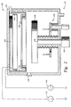
- FIG. 2 is high density plasma physical vapor deposition (HDP-PVD) chamber useful for forming the adhesion/encapsulation layer according to the present invention.
- An example of a HDP-PVD chamber is the IMP® chamber available from Applied Materials, Inc., Santa Clara, California.
- the HDP-PVD deposition chamber 100 generally includes a chamber enclosure 102, a substrate support member 104, a target 106, a shield 108 and a coil 110.
- the target 106 is disposed opposite of the substrate support member 104 and is electrically connected to a DC power supply 112.
- the shield 108 generally surrounds the region between the target 106 and the substrate support member 104 and is typically connected to a ground connection.
- the coil 110 is disposed interior of the shield 108 and is connected to an RF power supply 114.
- a gas inlet 116 disposed through the enclosure 102 introduces one or more processing gases into the chamber during processing.
- the substrate support member 104 is attached to an actuator shaft 118 disposed through the bottom of the enclosure 102.
- the actuator shaft 118 is connected to an actuator 120 which facilitates movement of the substrate support member 104 to various positions in the chamber.
- a slit valve 126 disposed on a sidewall of the enclosure 102 facilitates transfer of substrates into and out of the chamber.
- a substrate lift assembly 122 disposed relative to the substrate support member 104 facilitates positioning of a substrate onto and off of the substrate support member 104.
- the substrate support member 104 positions a substrate disposed thereon to a position below a cover ring 124 disposed on a lower portion of the shield 108 to shield the perimeter edge of the substrate from deposition.
- the adhesion/encapsulation layer according to the invention is preferably deposited using the following processing parameters in a high density plasma physical vapor deposition (HDP-PVD) chamber.
- the chamber pressure during the deposition process is preferably maintained between about 5 mT and about 100 mT, even more preferably between about 10 mT and about 30 mT.
- the target is preferably DC-biased at between about 1 kW and about 3 kW and between about 100V and about 300 V.
- the coil is preferably RF-biased at between about 1 kW and about 3 kW.
- the substrate support member preferably provides a substrate bias at between about 0W and about 500 W and between about 50V and about 300V.
- the adhesion/encapsulation layer is preferably deposited to a thickness between about 50 ⁇ and about 500 ⁇ for a feature having aperture width less than about 0.25 ⁇ m and an aspect ratio greater than about 5:1.
- an adhesion/encapsulation layer is deposited to about 300 ⁇ for a feature having dimensions of about 0.25 ⁇ m wide and about 2.5 ⁇ m deep.
- the heavy metals contemplated in the present invention provide low sticking coefficients and high resputtering rates when deposited using ionized metal plasma deposition techniques which enable better conformal coverage within high aspect ratio features compared to other metals ( i.e. , non-heavy metals).
- the adhesion/encapsulation layer according to the invention is also useful as the bottom electrode in a microelectronic device because the adhesion/encapsulation layer provides sufficient electrical conductivity.
- the electrode gate material and the adhesion layer for the dielectric layer are deposited with one process to improve efficiency and throughput of the system.
- the bottom electrode having the material according to the invention has a resistivity, ⁇ , less than about 500 ⁇ -cm, and even more preferably, less than about 250 ⁇ -cm.
- the dielectric layer 36 is deposited over the adhesion layer 40.
- the dielectric layer 36 comprises Ta 2 O 5 and is deposited using reactive sputtering techniques in a HDP-PVD chamber.
- the dielectric layer 36 is preferably deposited to a thickness between about 20 ⁇ and about 200 ⁇ , even more preferably between about 80 ⁇ and about 100 ⁇ .
- An adhesion/encapsulation layer 42 is then deposited over the dielectric layer 36.
- the adhesion/encapsulation layer 42 comprises the same material as the adhesion/encapsulation layer 40 (discussed above) and is deposited using IMP deposition techniques as described for the adhesion/encapsulation layer 40. It is believed that the materials listed above provide improved adhesion of the electrode material to the dielectric material because the adhesion/encapsulation layer comprises elements from the same or similar family of elements as the dielectric material. For example, the Ta based adhesion/encapsulation layer provides better adhesion to a dielectric material comprising Ta 2 O 5 .
- the second electrode 34 is formed over the adhesion/encapsulation layer 42 in the trench structure.
- the material of the second electrode fills the trench structure and is connected to the source region 22 of the access transistor of the DRAM device.
- the access transistor 20 of the DRAM device is formed above or adjacent a top portion of the trench capacitor using techniques generally known in the art.
- the adhesion/encapsulation layer 40 and 42 protect the dielectric layer 36 during a subsequent anneal process utilized to increases the dielectric constant of the dielectric layer.
- the anneal process can be performed in a variety of anneal chambers, including conventional furnace anneal chambers and rapid thermal anneal chambers. Anneal chambers in general are well known and commercially available. An example of an anneal chamber is the RTP XE plus Centura® thermal processor available from Applied Materials, Inc., Santa Clara, California. The inventors also contemplate using other commercially available thermal processors from manufacturers such as Eaton Corporation Thermal Processing Systems, Peabody, Massachusetts.
- the dielectric layer 36 is annealed at a temperature between about 500°C and about 800°C for between about 30 seconds and 120 seconds in a rapid thermal anneal process furnace. If annealed in a conventional thermal anneal furnace, the dielectric layer 36 is preferably annealed at a temperature between about 300°C and about 600°C for between about 5 minutes and 50 minutes.
- the present invention is useful in applications that benefit from an adhesion/encapsulation film having a relatively higher dielectric constant than currently practiced barrier/adhesion films.
- the film composition and properties of the TaN x and WN x films according to the invention provides a dielectric constant much closer to the high dielectric constant (HDC) materials such as Ta 2 O 5 , and thus, the overall effective dielectric constant of the adhesion layer, dielectric layer and encapsulation layer is not significantly lowered.
- the dielectric property of TaN x and WN x films increases generally with increase in the nitrogen content in these film ( i.e. , where x ⁇ 1).
- the TaN x and WN x films according to the invention are also useful as adhesion/encapsulation layers for other HDC materials. Furthermore, the inventors also contemplate depositing Ta or W in an oxygen environment or a combination of oxygen plus nitrogen environment to form films such as Ta x O y , Ta x O y N z , W x O y and W x O y N z for applications requiring dielectric films.
Landscapes
- Engineering & Computer Science (AREA)
- Manufacturing & Machinery (AREA)
- Semiconductor Memories (AREA)
- Electrodes Of Semiconductors (AREA)
- Fixed Capacitors And Capacitor Manufacturing Machines (AREA)
- Formation Of Insulating Films (AREA)
- Physical Deposition Of Substances That Are Components Of Semiconductor Devices (AREA)
- Physical Vapour Deposition (AREA)
Abstract
Description
Claims (20)
- A method for forming a microelectronic device, comprising:a) forming a first electrode;b) depositing an adhesion layer over the first electrode utilizing high density plasma physical vapor deposition, wherein the adhesion layer comprises a material selected from the group consisting of Ta, TaNx, W, WNx, Ta/TaNx, W/WNx, and combinations thereof;c) depositing a dielectric layer over the adhesion layer; andd) forming a second electrode over the dielectric layer.
- The method of claim 1, further comprising:e) depositing an encapsulation layer between the dielectric layer and the second electrode utilizing high density plasma physical vapor deposition, wherein the encapsulation layer comprises a material selected from the group consisting of Ta, TaNx, W, WNx, Ta/TaNx, W/WNx, and combinations thereof.
- The method of claim 1, further comprising:f) annealing the device in an anneal chamber.
- The method of claim 3 wherein the device is annealed at between about 300°C and about 600°C for between about 5 minutes and about 50 minutes in a conventional anneal furnace.
- The method of claim 3 wherein the device is annealed at between about 500°C and about 800°C for between about 30 seconds and about 120 seconds in a rapid thermal anneal processor.
- The method of claim 1 wherein the dielectric layer comprises Ta2O5 deposited using reactive sputtering deposition techniques.
- The method of claim 1 wherein the microelectronic device is formed within a trench-type feature on a semiconductor substrate.
- The method of claim 1 wherein the adhesion layer is deposited in a high density plasma physical vapor deposition chamber at a chamber pressure between about 5mT and about 100mT.
- The method of claim 1 wherein the HDP-PVD chamber includes a target biased between about 1kW and 3kW and between about 100V and about 300V.
- The method of claim 1 wherein the HDP-PVD chamber includes a substrate support member biased between about 0W and 500W and between about 50V and 300V.
- The method of claim 1 wherein the HDP-PVD chamber includes a coil that is RF biased between about 1kW and about 3kW.
- A microelectronic device, comprising:a) a first electrode;b) a second electrode;c) a dielectric layer disposed between the first and second electrodes; andd) an adhesion layer disposed between the first electrode and the dielectric layer, wherein the adhesion layer comprises a material selected from the group consisting of Ta, TaNx, W, WNx, Ta/TaNx, W/WNx, and combinations thereof.
- The microelectronic device of claim 12 wherein the dielectric layer comprises a high dielectric constant material.
- The microelectronic device of claim 12 wherein the dielectric layer comprises Ta2O5.
- The microelectronic device of claim 12 wherein the microelectronic device comprises a trench capacitor.
- The microelectronic device of claim 15 wherein the first electrode comprises a doped substrate having a surface forming a bottom of a trench structure.
- The microelectronic device of claim 15 wherein the adhesion layer covers a surface of the trench structure.
- The microelectronic device of claim 12, further comprising:e) an encapsulation layer disposed between the dielectric layer and the second electrode, wherein the adhesion layer comprises a material selected from the group consisting of Ta, TaNx, W, WNx, Ta/TaNx, W/WNx, and combinations thereof.
- The microelectronic device of claim 12 wherein the first electrode comprises a material selected from the group consisting of Ta, TaNx, W, WNx, Ta/TaNx, W/WNx, and combinations thereof.
- The microelectronic device of claim 12 wherein the first electrode and the adhesion layer comprise a same material selected from the group consisting of Ta, TaNx, W, WNx, Ta/TaNx, W/WNx, and combinations thereof.
Applications Claiming Priority (2)
| Application Number | Priority Date | Filing Date | Title |
|---|---|---|---|
| US362923 | 1999-07-27 | ||
| US09/362,923 US6313033B1 (en) | 1999-07-27 | 1999-07-27 | Ionized metal plasma Ta, TaNx, W, and WNx liners for gate electrode applications |
Publications (2)
| Publication Number | Publication Date |
|---|---|
| EP1073102A2 true EP1073102A2 (en) | 2001-01-31 |
| EP1073102A3 EP1073102A3 (en) | 2001-10-31 |
Family
ID=23428071
Family Applications (1)
| Application Number | Title | Priority Date | Filing Date |
|---|---|---|---|
| EP00114985A Withdrawn EP1073102A3 (en) | 1999-07-27 | 2000-07-20 | Liners formed by ionized metal plasma deposition for gate electrode applications |
Country Status (5)
| Country | Link |
|---|---|
| US (1) | US6313033B1 (en) |
| EP (1) | EP1073102A3 (en) |
| JP (1) | JP2001102548A (en) |
| KR (1) | KR20010021130A (en) |
| TW (1) | TW454247B (en) |
Cited By (1)
| Publication number | Priority date | Publication date | Assignee | Title |
|---|---|---|---|---|
| EP1094504A3 (en) * | 1999-10-18 | 2001-08-22 | Applied Materials, Inc. | PVD-IMP tungsten and tungsten nitride as a liner, barrier, and/or seed layer |
Families Citing this family (11)
| Publication number | Priority date | Publication date | Assignee | Title |
|---|---|---|---|---|
| US6174811B1 (en) | 1998-12-02 | 2001-01-16 | Applied Materials, Inc. | Integrated deposition process for copper metallization |
| US20030107111A1 (en) | 2001-12-10 | 2003-06-12 | International Business Machines Corporation | A 3-d microelectronic structure including a vertical thermal nitride mask |
| US6723611B2 (en) * | 2002-09-10 | 2004-04-20 | International Business Machines Corporation | Vertical hard mask |
| JP4275395B2 (en) * | 2002-12-11 | 2009-06-10 | 株式会社ルネサステクノロジ | Manufacturing method of semiconductor device |
| US7030430B2 (en) * | 2003-08-15 | 2006-04-18 | Intel Corporation | Transition metal alloys for use as a gate electrode and devices incorporating these alloys |
| US7550381B2 (en) * | 2005-07-18 | 2009-06-23 | Applied Materials, Inc. | Contact clean by remote plasma and repair of silicide surface |
| JP2013057616A (en) | 2011-09-09 | 2013-03-28 | Azbil Corp | Environment sensor |
| US8796751B2 (en) | 2012-11-20 | 2014-08-05 | Micron Technology, Inc. | Transistors, memory cells and semiconductor constructions |
| US12176386B2 (en) * | 2022-05-24 | 2024-12-24 | Nanya Technology Corporation | Storage capacitor with multiple dielectrics |
| US20230402499A1 (en) * | 2022-06-08 | 2023-12-14 | Intel Corporation | High density metal layers in electrode stacks for transition metal oxide dielectric capacitors |
| CN117373829A (en) * | 2023-12-08 | 2024-01-09 | 深圳市汉嵙新材料技术有限公司 | Thin film capacitor, method of manufacturing the same, and semiconductor device |
Family Cites Families (19)
| Publication number | Priority date | Publication date | Assignee | Title |
|---|---|---|---|---|
| EP0024863B1 (en) | 1979-08-31 | 1983-05-25 | Fujitsu Limited | A tantalum thin film capacitor and process for producing the same |
| US4760369A (en) | 1985-08-23 | 1988-07-26 | Texas Instruments Incorporated | Thin film resistor and method |
| US4649625A (en) | 1985-10-21 | 1987-03-17 | International Business Machines Corporation | Dynamic memory device having a single-crystal transistor on a trench capacitor structure and a fabrication method therefor |
| US4753851A (en) * | 1987-05-29 | 1988-06-28 | Harris | Multiple layer, tungsten/titanium/titanium nitride adhesion/diffusion barrier layer structure for gold-base microcircuit interconnection |
| US5225363A (en) | 1988-06-28 | 1993-07-06 | Texas Instruments Incorporated | Trench capacitor DRAM cell and method of manufacture |
| KR930011538B1 (en) * | 1991-07-16 | 1993-12-10 | 한국과학기술연구원 | Tungsten Nitride Thin Film Deposition Method for Metallization of Silicon Semiconductor Devices |
| US5142438A (en) | 1991-11-15 | 1992-08-25 | Micron Technology, Inc. | Dram cell having a stacked capacitor with a tantalum lower plate, a tantalum oxide dielectric layer, and a silicide buried contact |
| JP2786071B2 (en) | 1993-02-17 | 1998-08-13 | 日本電気株式会社 | Method for manufacturing semiconductor device |
| JP2679599B2 (en) | 1993-12-02 | 1997-11-19 | 日本電気株式会社 | Method for manufacturing semiconductor device |
| DE69531170T2 (en) * | 1994-11-30 | 2004-05-06 | Micron Technology, Inc. | Uneven semiconductor storage capacitor |
| US5614437A (en) | 1995-01-26 | 1997-03-25 | Lsi Logic Corporation | Method for fabricating reliable metallization with Ta-Si-N barrier for semiconductors |
| JP3127348B2 (en) | 1995-02-27 | 2001-01-22 | エルジイ・セミコン・カンパニイ・リミテッド | Manufacturing method of semiconductor device using tungsten film having uneven surface shape |
| US5668040A (en) * | 1995-03-20 | 1997-09-16 | Lg Semicon Co., Ltd. | Method for forming a semiconductor device electrode which also serves as a diffusion barrier |
| US5717628A (en) | 1996-03-04 | 1998-02-10 | Siemens Aktiengesellschaft | Nitride cap formation in a DRAM trench capacitor |
| US5654233A (en) * | 1996-04-08 | 1997-08-05 | Taiwan Semiconductor Manufacturing Company Ltd | Step coverage enhancement process for sub half micron contact/via |
| US5633200A (en) | 1996-05-24 | 1997-05-27 | Micron Technology, Inc. | Process for manufacturing a large grain tungsten nitride film and process for manufacturing a lightly nitrided titanium salicide diffusion barrier with a large grain tungsten nitride cover layer |
| TW421858B (en) * | 1997-06-30 | 2001-02-11 | Texas Instruments Inc | Integrated circuit capacitor and memory |
| US6140228A (en) * | 1997-11-13 | 2000-10-31 | Cypress Semiconductor Corporation | Low temperature metallization process |
| US6201276B1 (en) * | 1998-07-14 | 2001-03-13 | Micron Technology, Inc. | Method of fabricating semiconductor devices utilizing in situ passivation of dielectric thin films |
-
1999
- 1999-07-27 US US09/362,923 patent/US6313033B1/en not_active Expired - Fee Related
-
2000
- 2000-07-12 TW TW089113910A patent/TW454247B/en not_active IP Right Cessation
- 2000-07-20 EP EP00114985A patent/EP1073102A3/en not_active Withdrawn
- 2000-07-25 JP JP2000224020A patent/JP2001102548A/en not_active Withdrawn
- 2000-07-26 KR KR1020000042989A patent/KR20010021130A/en not_active Withdrawn
Cited By (1)
| Publication number | Priority date | Publication date | Assignee | Title |
|---|---|---|---|---|
| EP1094504A3 (en) * | 1999-10-18 | 2001-08-22 | Applied Materials, Inc. | PVD-IMP tungsten and tungsten nitride as a liner, barrier, and/or seed layer |
Also Published As
| Publication number | Publication date |
|---|---|
| JP2001102548A (en) | 2001-04-13 |
| US6313033B1 (en) | 2001-11-06 |
| TW454247B (en) | 2001-09-11 |
| KR20010021130A (en) | 2001-03-15 |
| EP1073102A3 (en) | 2001-10-31 |
Similar Documents
| Publication | Publication Date | Title |
|---|---|---|
| US7432184B2 (en) | Integrated PVD system using designated PVD chambers | |
| US6489199B2 (en) | Multiple step methods for forming conformal layers | |
| JP4314413B2 (en) | Ta ▲ Lower2 ▼ O ▲ Lower5 Dielectric layer manufacturing method | |
| US6909137B2 (en) | Method of creating deep trench capacitor using a P+ metal electrode | |
| EP1127956A2 (en) | Tantalum nitride CVD deposition by tantalum oxide densification | |
| US6730954B2 (en) | Method of depositing tungsten nitride using a source gas comprising silicon | |
| US5918118A (en) | Dual deposition methods for forming contact metallizations, capacitors, and memory devices | |
| US6313033B1 (en) | Ionized metal plasma Ta, TaNx, W, and WNx liners for gate electrode applications | |
| US20020030218A1 (en) | Method of making a thin film capacitor with an improved top electrode | |
| US6337274B1 (en) | Methods of forming buried bit line memory circuitry | |
| US7498628B2 (en) | Capacitor for a semiconductor device and manufacturing method thereof | |
| US6815753B2 (en) | Semiconductor capacitor structure and method to form same | |
| US6010961A (en) | Methods of establishing electrical communication with substrate node locations, semiconductor processing methods of forming dynamic random access memory (DRAM) circuitry, and semiconductor assemblies | |
| US20020001946A1 (en) | Method and fabricating metal interconnection with reliability using ionized physical vapor deposition | |
| US6365487B2 (en) | Method of manufacturing a capacitor in a semiconductor device | |
| US20060017090A1 (en) | Semiconductor device and method of manufacturing the same | |
| US20030119325A1 (en) | Method of forming a metal line in a semiconductor device | |
| US20020011620A1 (en) | Capacitor having a TaON dielectric film in a semiconductor device and a method for manufacturing the same | |
| US6245631B1 (en) | Method of forming buried bit line memory circuitry and semiconductor processing method of forming a conductive line | |
| US6734488B1 (en) | Semiconductor device and manufacturing method thereof | |
| US6919269B2 (en) | Production method for a semiconductor component | |
| JP3120867B2 (en) | Semiconductor device including capacitance element and method of manufacturing the same | |
| JP2000307069A (en) | Method for manufacturing semiconductor device | |
| US20050181600A1 (en) | Method of forming a semiconductor device having a Ti/TiN/Ti<002>/a1<111> laminate |
Legal Events
| Date | Code | Title | Description |
|---|---|---|---|
| PUAI | Public reference made under article 153(3) epc to a published international application that has entered the european phase |
Free format text: ORIGINAL CODE: 0009012 |
|
| AK | Designated contracting states |
Kind code of ref document: A2 Designated state(s): AT BE CH CY DE DK ES FI FR GB GR IE IT LI LU MC NL PT SE |
|
| AX | Request for extension of the european patent |
Free format text: AL;LT;LV;MK;RO;SI |
|
| PUAL | Search report despatched |
Free format text: ORIGINAL CODE: 0009013 |
|
| AK | Designated contracting states |
Kind code of ref document: A3 Designated state(s): AT BE CH CY DE DK ES FI FR GB GR IE IT LI LU MC NL PT SE |
|
| AX | Request for extension of the european patent |
Free format text: AL;LT;LV;MK;RO;SI |
|
| AKX | Designation fees paid | ||
| REG | Reference to a national code |
Ref country code: DE Ref legal event code: 8566 |
|
| STAA | Information on the status of an ep patent application or granted ep patent |
Free format text: STATUS: THE APPLICATION IS DEEMED TO BE WITHDRAWN |
|
| 18D | Application deemed to be withdrawn |
Effective date: 20020503 |