EP1071273A2 - Data flow control and storage facility for an image reproduction system - Google Patents
Data flow control and storage facility for an image reproduction system Download PDFInfo
- Publication number
- EP1071273A2 EP1071273A2 EP00305810A EP00305810A EP1071273A2 EP 1071273 A2 EP1071273 A2 EP 1071273A2 EP 00305810 A EP00305810 A EP 00305810A EP 00305810 A EP00305810 A EP 00305810A EP 1071273 A2 EP1071273 A2 EP 1071273A2
- Authority
- EP
- European Patent Office
- Prior art keywords
- image data
- controller
- digital
- secondary storage
- image
- Prior art date
- Legal status (The legal status is an assumption and is not a legal conclusion. Google has not performed a legal analysis and makes no representation as to the accuracy of the status listed.)
- Granted
Links
Images




Classifications
-
- H—ELECTRICITY
- H04—ELECTRIC COMMUNICATION TECHNIQUE
- H04N—PICTORIAL COMMUNICATION, e.g. TELEVISION
- H04N1/00—Scanning, transmission or reproduction of documents or the like, e.g. facsimile transmission; Details thereof
- H04N1/32—Circuits or arrangements for control or supervision between transmitter and receiver or between image input and image output device, e.g. between a still-image camera and its memory or between a still-image camera and a printer device
- H04N1/32561—Circuits or arrangements for control or supervision between transmitter and receiver or between image input and image output device, e.g. between a still-image camera and its memory or between a still-image camera and a printer device using a programmed control device, e.g. a microprocessor
-
- H—ELECTRICITY
- H04—ELECTRIC COMMUNICATION TECHNIQUE
- H04N—PICTORIAL COMMUNICATION, e.g. TELEVISION
- H04N1/00—Scanning, transmission or reproduction of documents or the like, e.g. facsimile transmission; Details thereof
- H04N1/32—Circuits or arrangements for control or supervision between transmitter and receiver or between image input and image output device, e.g. between a still-image camera and its memory or between a still-image camera and a printer device
- H04N1/32358—Circuits or arrangements for control or supervision between transmitter and receiver or between image input and image output device, e.g. between a still-image camera and its memory or between a still-image camera and a printer device using picture signal storage, e.g. at transmitter
-
- H—ELECTRICITY
- H04—ELECTRIC COMMUNICATION TECHNIQUE
- H04N—PICTORIAL COMMUNICATION, e.g. TELEVISION
- H04N2201/00—Indexing scheme relating to scanning, transmission or reproduction of documents or the like, and to details thereof
- H04N2201/0077—Types of the still picture apparatus
- H04N2201/0081—Image reader
-
- H—ELECTRICITY
- H04—ELECTRIC COMMUNICATION TECHNIQUE
- H04N—PICTORIAL COMMUNICATION, e.g. TELEVISION
- H04N2201/00—Indexing scheme relating to scanning, transmission or reproduction of documents or the like, and to details thereof
- H04N2201/0077—Types of the still picture apparatus
- H04N2201/0082—Image hardcopy reproducer
-
- H—ELECTRICITY
- H04—ELECTRIC COMMUNICATION TECHNIQUE
- H04N—PICTORIAL COMMUNICATION, e.g. TELEVISION
- H04N2201/00—Indexing scheme relating to scanning, transmission or reproduction of documents or the like, and to details thereof
- H04N2201/0077—Types of the still picture apparatus
- H04N2201/0087—Image storage device
Definitions
- the invention relates to improved image reproduction systems. More particularly, the invention is directed to a data flow control and storage facility for reducing the amount of electronic memory in an image reproduction system.
- Electrophotographic copiers such as digital copiers
- a digital copier an input scanning facility captures a document image, and converts the captured image into digital data.
- a control unit then compresses the image data and either forwards the compressed data to a suitable printing facility, or stores the data in a system memory.
- System memory typically includes both magnetic disk storage and electronic storage.
- electronic storage consists of random access memory (RAM) devices, such as DRAM.
- RAM random access memory
- DRAM is used essentially as a page buffer for intermediate storage of image data.
- conventional copiers spool image data from DRAM to magnetic disk memory during scanning. Subsequently, the copier spools the image data from magnetic disk back to DRAM for printing.
- conventional high-performance SCSI-based disk subsystems operate disk controllers as bus masters. Operating in master mode, the disk controller can increase the rate with which data is spooled between magnetic disk memory and DRAM.
- conventional copiers continue to employ large amounts of expensive DRAM, and to waste significant time performing spooling operations.
- control and storage facility includes a digital communication bus, a secondary storage device, an image output controller, an image input controller and a secondary storage controller.
- the image output controller, image input controller and secondary storage controller are in digital communication over the digital communication bus.
- the secondary storage device and the secondary storage controller communicate by way of an SCSI interface.
- the secondary storage device may be magnetic tape, magnetic disk, optical disk, solid state memory or any other type of digital storage other than DRAM.
- the invention thus reduces system costs by reducing the amount of DRAM required to operate image reproduction systems.
- the invention also increases the speed with which image data can be transferred by reducing the number of spooling operations.
- the digital communication bus optionally a PCI-type bus, transfers digital image data in the image reproduction system.
- the secondary storage device stores the digital image data.
- the image output controller receives digital image data by way of the digital communication bus and can output the received digital image data to an external destination.
- the image input controller is adapted for receiving digital image data from an external source and for transferring the received digital image data by way of the digital communication bus.
- the secondary storage controller is adapted for transferring digital image data directly from the secondary storage device to the image output controller by way of the digital communication bus.
- the secondary storage controller is also adapted for transferring digital image data directly from the image input controller to the secondary storage device.
- the secondary storage controller operates in master mode to gain control of the digital communication bus, and transfers blocks of digital image data in a burst format.
- the secondary storage controller includes a buffer cache memory having a write buffer portion and a read buffer portion.
- the write buffer portion can accumulate a block of digital image data for direct transfer from the image input controller to the secondary storage device.
- the read buffer portion can accumulate a block of digital image data for direct transfer from the secondary storage device to the image input controller.
- the buffer cache memory is a FIFO-type cache memory.
- the image output controller includes an output cache memory for accumulating a block of digital image data for outputting.
- the secondary storage controller includes a read master controller. The read master controller determines whether the output cache memory has enough storage available to receive a block of digital image data. In response to determining that enough storage is available, the master controller writes a block of digital image data from the read buffer portion of the buffer cache memory directly to the output cache memory.
- the read master controller queries the image output controller to determine whether the output cache memory has enough storage available to receive a block of digital image data.
- the image output controller includes output control elements in digital communication with the output cache memory and with the digital communication bus.
- the output control elements signal the read master controller regarding whether there is enough storage available in the output cache memory to receive a block of digital image data.
- the output control elements signal a PCI-type disconnect to the read master controller in response to the output cache memory having insufficient storage available.
- the image input controller includes an input cache memory for accumulating a block of digital image data for transfer to the write buffer portion of the buffer cache memory.
- the secondary storage controller includes a write master controller for determining whether the input cache memory has accumulated a block of digital image data. In response to determining that a block of digital image data has been accumulated, the write master controller transfers the block of digital image data directly from the input cache memory to the input buffer portion of the buffer cache.
- the write master controller signals the image input controller to determine whether the input cache memory has accumulated a block of image data.
- the image output controller includes input control elements in digital communication with the input cache memory and with the digital communication bus.
- the input control elements signal the write master controller with a PCI-type disconnect, without transferring any image data.
- control and storage facility of the invention includes a loop-back channel controller in digital communication with the digital communication bus and adapted for receiving digital image data by way of the digital communication bus and for outputting the received digital image data for additional processing. Additionally, the secondary storage controller is further adapted for transferring digital image data directly to the loop-back channel controller by way of the digital communication bus.
- control and storage facility includes a secondary storage device for storing image data within an image reproduction system; elements for transferring image data from a source external to the control and storage facility to the secondary storage device, without intermediately storing the image data in DRAM; and elements for transferring the image data from the secondary storage device to a destination, external to the control and storage facility, without intermediately storing the image data in a DRAM.
- control and storage facility includes a secondary storage device for storing image data within the image reproduction system; elements for transferring image data, optically scanned into the image reproduction system, into the secondary storage device without intermediately storing the image data in a DRAM buffer; and elements for transferring the image data, stored in the secondary storage device, to an image data output interface of the image reproduction system, without intermediately storing the image data in a DRAM buffer.
- the invention comprises a method of transferring image data in an image reproduction system.
- the method includes the steps of transferring digital image data from an image input section of the image reproduction system directly to a secondary storage device, without intermediately storing the digital image data in a DRAM buffer; and transferring the image data from the secondary storage device to an image output section of the image reproduction system, without intermediately storing the digital image data in a DRAM buffer.
- image data can be transferred directly from an input interface, such as an optical scanner interface, to a secondary storage device, such as magnetic or optional memory, without intermediately storing the scanned image data in a DRAM buffer.
- image data can be transferred directly from the secondary storage device to an output interface, such as a printer interface or a supplemental processor interface, also without being stored intermediately in a DRAM buffer.
- the invention provides a system for improving data flow in an image forming or reproduction system by eliminating or reducing intermediate data transfers between secondary memory and electronic memory.
- the invention also provides a system for reducing the amount of electronic memory used in image forming or reproduction systems by transferring image data directly between the secondary memory and I/O devices. This approach provides an advantage over conventional systems, which repeatedly spool image data between the secondary memory and electronic memory, such as DRAM, thus using the DRAM as a page buffer.
- the invention can be employed in a number of different types of image forming or reproduction systems, examples of which include electrophotographic, electrostatic, ionographic, and the like, which are adapted to capture and/or store image data associated with a particular object, such as a document.
- the system of the invention is intended to be implemented in a variety of environments, such as in any of the foregoing types of image reproduction systems, and is not limited to the specific system described herein. Although, in the illustrative embodiments, a system and method of the invention are described in the context of a digital image copier, the invention is not intended to be limited to such techniques.
- FIG. 1 provides a simplified image flow diagram of an exemplary digital image copier 10 suitable for employing a data flow control and storage facility according to the teachings of the invention.
- the copier 10 includes an image input section 12, a control section 16, and an image output section 18.
- the copier 10 also includes a system memory 20.
- the input section 12 is adapted for acquiring or receiving an image of a document. Subsequent to acquiring or receiving a document image, the input section 12 transfers the image data to the system memory section 20.
- the system memory 20 can include any suitable non-DRAM secondary storage elements adapted for storing image data. According to the illustrative embodiment of the invention, the system memory 20 is preferably magnetic disk memory.
- the system memory may include, but is not limited to, optical disks, magnetic tape or non-DRAM solid state memory.
- the control section 16 includes elements for controlling the transfer of image data from the input section 12 to the system memory 20, as well as for controlling the transfer of the image data from the system memory 20 to the image output section 18.
- the control stage 16 is depicted logically as a separate block, the control section 16 can be distributed throughout the copier 10.
- the illustrated image output section 18 can include any suitable apparatus for reproducing the image on a substrate, such as a conventional printer or copier, both of which are known and well characterized in the art.
- FIG 2 is a perspective view of the general purpose digital image copier 10 of Figure 1.
- the digital image copier 10 employs a data flow control and storage facility according to the teachings of the invention.
- the illustrated digital image copier 10 for purposes of explanation, is once again logically divided into multiple sections according to functionality. As illustrated in Figure 1, those sections include an image input section 12, a control section 16, and an image output section 18.
- the image input section 12 includes both local (i.e., on-site) and remote image input interfaces, thus enabling the system 10 to provide network, scan, and print services in a single integrated system.
- the invention also contemplates using other types of printing systems.
- the image output section 18 can instead employ an ink jet printer, an ionographic printer, a thermal printer, a photographic printer and the like.
- the image output section 18 can be incorporated in electronic display systems, such as CRTs, LCD's, LED's, or other like image scanning, processing, or recording systems, or alternatively, other signal transmitting, receiving and recording systems.
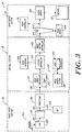
- FIG 3 is a logical block diagram depicting the major components of the digital image copier 10 of Figures 1 and 2.
- the system 10 is logically apportioned into the image input section 12, the control section 16 and the output section 18.
- the locations of the various elements shown in sections 12, 16 and 18 can be rearranged without affecting the operation of the copier 10.
- the image input section 12 includes a network interface 22 for remote or off-site transmission of image data into the copier 10.
- the network interface 22 preferably includes a suitable communication channel, such as a telephone line, for enabling image data to be transferred into the image input section 12 from one or more remote sources.
- Alternate embodiments of the invention include remote image data sources, such as streaming tape, floppy disk, video camera, and the like.
- the image input section 12 includes a document scanner 24 that optionally employs a universal or automatic document handler (not shown) for the purpose of automatically and sequentially placing and locating documents for scanning.
- the document scanner 24 provides manual document mode and/or a computer forms feeder (CFF) mode, the latter to accommodate documents in the form of computer fanfold.
- CFF computer forms feeder
- the scanner 32 incorporates one or more linear light sensitive or photoelectric arrays 26, such as the illustrated charge-coupled device (CCD), for reciprocating scanning movement below a glass platen 28.
- An associated optical arrangement focuses light reflected from a document on the platen 28 onto the photoelectric array 26.
- the photoelectric array 26 in response, generates electric image output signals 30 (e.g., pixels) and couples those signals to an analog-to-digital converter 32 for conversion into digital image data or signals 34.
- the converter 32 then couples the digital image signals 34 to a processor 36 for further processing.
- the illustrated processor 36 places the digital image data 34 in condition for printing by enhancing and/or altering the digital image data 34.
- the processor 36 can perform filtering, threshholding, screening, cropping, scaling and related functions. Following any changes or adjustments, the processor 36 forwards the conditioned digital image data 38 to the control section 16.
- the network interface 22 conveys remotely received image data signals 40 to the processor 36 for manipulation and forwarding to the control section 16.
- the system memory 20 is included in the discussion of the control section 16.
- the control section 16 includes an image input controller 42, a user interface 44, a system controller 46, the system memory 20, an image manipulation section 48, an image compression section 50, and an image output controller 52.
- the image input controller 42 receives the digital image data 38 from the processor 36.
- the image compression section 50 compresses the image data 38 according to known compression algorithms.
- the compression section 50 also segments the image data 38 into slices that are (n) scan lines wide; each slice having a slice pointer.
- the image input controller 42 stores the compressed image data 56, together with the slice pointers and any related image descriptors providing image specific information (such as height and width of the document in pixels, the compression method used, pointers to the compressed image data, and pointers to the image slice pointers), to an image file.
- image files representing different print jobs can be stored in the system memory 20.
- the user interface 44 includes a combined controller/display consisting of an interactive touch screen 56, a keyboard 58 and a mouse 60.
- the user interface 44 preferably enables the operator to interface with the output section 18, to program print jobs; execute instructions; and obtain system operating information, instructions, programming information and icons, diagnostic information, visual document facsimile display and pictorial views, and the like.
- Items displayed on the touch screen 56, such as files and icons, are actuated by either touching the displayed item on the screen 56 or by using the mouse 60 to manipulate a cursor to select an item.
- the system memory 20 includes a plurality of magnetic memory disks for storing the compressed image data 54, as well as other data known in the art, such as machine operating system software, machine operating data and the like.
- the system controller 46 directs transfer of the image data 54 stored in the system memory 20. If processing other than that provided by the processor 36 is required, the system controller 46 transfers the image data 54 to the image manipulation section 48.
- the image manipulation section 48 performs additional processing, such as collation, decomposition, and related formatting operations. Following the additional processing, the system controller 46 returns the image data 54 to the system memory 20. Additionally, the system controller 46 can transfer the image data 54 to the user interface 44 for display, or to the image output controller 52 for printing.
- the image output controller 52 decompresses and readies the image data 54 for printing, and then forwards the print-ready image data 62 to the image output section 18.
- the system controller 46 purges the image data 54 from the system memory 20, subsequent to that data being received by the printer stage 28.
- the illustrated image output section 18 is logically divided into a raster output scanner (ROS) section 64, a print module 66, a paper supply section 68, and a finisher section 70.
- the ROS section 64 employs a radiation source, such as a laser, to provide one or more imaging beams that are scanned across a moving photoreceptor of the print module 66 by any suitable structure, such as by a rotating polygon. This creates a latent electrostatic image on portions of a photoreceptor, which can be subsequently developed by a developer stage in accordance with known techniques, and then transferred to a print media delivered by the paper supply section 68.
- the print media can include various known substrates which are capable of accepting an image.
- Example substrates include transparencies, preprinted sheets, vellum, glossy covered stock, film and the like.
- the print media can also include any of a variety of sheet sizes, types, and colors, and for this, plural media supply trays of the paper supply section 68 can be provided.
- the developed image transferred to the print media is permanently fixed or fused and the resulting prints discharged to either an output tray or to the finisher 70.
- the finisher 70 provides certain finishing selections, such as a stitcher for stitching the prints together to form books, a thermal binder for adhesively binding the prints into books, and/or other finishing options such as stapling, slitting, perforating, saddle stitching, folding, trimming, or the like.
- system control functions embodied in the schematic representation of the system controller 46 can be distributed throughout the illustrated digital image copier 10.
- the copier 10 may employ an optional print controller 72 to control the printer functions and operations in accordance with selected job program parameters.
- an operator provides such job program parameters by way of the user interface 44.
- program parameters are derived from sensor signals and processes within the image output section 18.
- DRAM dynamic random access memory
- a disk controller operating as a bus master, typically spools the image data from the DRAM page buffer to magnetic disk memory. Subsequently, during printing, the disk controller typically spools the image data back from the magnetic disk memory to the DRAM page buffer.
- a system embodying features of the invention reduces the amount of DRAM required for scanning and/or printing the image data by eliminating the DRAM page buffer.
- an illustrative embodiment of the invention can significantly reduce or eliminate the use of any DRAM.
- the invention achieves this enhancement by writing the scanned image data from the image input section 12 directly to the system memory 20, without intermediately writing the data to a DRAM page buffer. Hence, the system avoids the use of an intermediate, costly memory device.
- the invention transfers the image data back from the system memory 20 to the image output section 18.
- the invention utilizes features of the PCI bus to perform burst transfers of blocks of image data between the system memory 20 and I/O devices, such as scanners and printers.
- FIG 4 is a logical block diagram of a data flow control and storage facility 15 (hereinafter "the facility 15") according to an illustrative embodiment of the invention.
- the illustrated facility 15 has a number of components in common with the control section 16 of Figure 3. More particularly, the facility 15 includes a video ASIC 74 and a memory controller ASIC 76, coupled together over a PCI bus 78.
- the illustrated facility 15 also includes the system memory 20, coupled to the memory controller ASIC 76 by way of an SCSI interface 80.
- the illustrated video ASIC 74 includes the image input controller 42, the image output controller 52 of the control section 16, along with a loop-back channel controller 82.
- a target decode and control network section 84 provides, among other functions, address decoding logic for the image input controller 42, the image output controller 52 and the loop-back channel controller 82.
- the facility 15 of Figure 4 can transfer image data between the system memory 20 and any of the image input section 12, the image output section 18 and additional processing resources 85, by way of the PCI bus 78 and the memory controller ASIC 76.
- the memory controller ASIC 76 in response to a scan operation being initiated, gains control of the PCI bus 78, and requests a block of data from the image input controller 42. Until the input controller 42 has a block of image data to transfer, the controller generates and forwards disconnect signals to the memory controller ASIC 76 by way of the PCI bus 78. Once the image input controller 42 has received a block of image data from the image input section 12, it transfers the image data onto the PCI bus 78. The memory controller ASIC 76 thus receives the block of data and stores it to the system memory 20 by way of the SCSI interface 90.
- the memory controller ASIC 76 In response to the initiation of a print operation, once again, the memory controller ASIC 76, operating in master mode, gains control of the PCI bus 78. Subsequent to gaining control of the PCI bus 78, the memory controller ASIC 76 signals the image output controller 52 to determined if the image output controller 52 has sufficient memory available to receive a block of image data. If the image output controller 52 does not have a sufficient amount of memory available to accept the memory controller ASIC's programmed block size, the image output controller generates a disconnect signal and forwards it to the memory controller ASIC 76 over the PCI bus 78.
- the image output controller 52 If the image output controller 52 has enough memory available to accommodate a block of data from the memory controller ASIC 76, it ceases transmission of the disconnect signals and receives the block of image data. The image output controller 52 then transfers the received block of data to the image output section 18. As soon as the image output controller 52 frees up sufficient memory, it once again can receive a block of image data from the memory controller ASIC 76.
- the facility 15 also provides a loop-back channel controller 82.
- the loop-back controller 82 operates in essentially the same fashion as the image output controller 52.
- the memory controller ASIC 76 operating in master mode, can transfer the image data, a block at a time, from the system memory 20 to the loop-back controller 82.
- the loop-back controller 82 generates a disconnect signal until it has sufficient memory free to accommodate a block of image data from the memory controller ASIC 76.
- the loop-back controller 82 transfers the block of image data to the additional processing resources 85.
- the additional processing resources 85 can include the image manipulation section 48, also shown in Figure 3, as well as other resources obvious to those of ordinary skill in the art.
- the additional processing resources 85 transfer the image data back to the loop-back channel controller 82.
- the loop-back channel controller 82 forwards the image data to the input image controller 42.
- the memory controller ASIC 76 requests the image data from the input controller 42 in the same fashion as if the data was received from a scan operation.
- the memory controller ASIC 76 performs data transfers between the system memory 20 and the controllers 42, 52 and 82 using a data burst transfer scheme. Burst transfers over the PCI bus 78 are well characterized in the art. However, according to other embodiments, other transfer protocols can be employed, such as SBUS transfers.
- the target decode and control logic 84 provides, among other functions, address decoding for buffer memory included in the image output controller 52, the image input controller 42 and the loop-back controller 82.
- FIG. 5 is a more detailed logical block diagram of the facility 15 of Figure 4.
- the facility 15 includes a memory controller ASIC 76, an image data ASIC 74, a system memory 20 and additional image data processing resources 48.
- the memory controller ASIC 76 operating in master mode, communicates with the image data ASIC 82 over a PCI bus 78.
- the memory controller ASIC 76 communicates with the system memory 20 by way of an SCSI interface 80.
- the memory controller ASIC 76 operating in master mode, controls the transfer of image data between the magnetic disk storage unit 20 and the image data ASIC 74.
- the image data ASIC 74 interfaces between PCI bus 78 and the image input section 12, the image output section 18, and the additional processing resources 85.
- the memory controller ASIC 74 includes a write buffer 87, a read buffer 86, a media controller 88, and PCI read and write bus masters 90 and 92.
- the write buffer 87 stores blocks of data during burst data transfers from the PCI bus 78 to the system memory 20.
- the read buffer 86 stores blocks of data during burst data transfers from the system memory 20 to the PCI bus 78.
- the image data ASIC 74 includes the image input controller 42, the image output controller 52, the loop-back channel controller 82 and the target decode and control logic 84, as illustrated in Figure 4.
- the image output controller 52 includes a write FIFO memory 94, a write master controller 96, and optionally includes a decompression network 98.
- the image input controller 42 includes a read FIFO memory 100, a read master controller 102, and optionally includes a compression network 104.
- the image input controller 42 also includes a multiplexer 106 for selecting between a signal from the image input section 12 and the loop-back controller 82.
- the loop-back controller 82 includes a loop FIFO memory 108, a loopback master controller 110 and external interface logic 112.
- the read and write FIFOs 100 and 94 map to selected memory addresses and operate essentially like cache memory.
- the write FIFO 94 accepts the image data transferred by the disk controller ASIC 76 from the system memory 20 to the image output section 18.
- the read FIFO 100 accepts the image data transferred by the memory controller ASIC 76 from the image input section 12 to the system memory 20.
- the FIFOs 100 and 94 are between about 128-bytes and 8 M-bytes. Even at 8 M-bytes, the relatively inexpensive FIFOs 100 and 94 provide considerable cost savings over the prior 256 M-byte DRAM page buffers.
- the present invention avoids the need of placing expensive memory devices, such as DRAM, between the image data ASIC 74 and the PCI bus 78.
- the multiplexer 106 buffers the image data from the image input section 12 into the image data ASIC 74.
- the multiplexer 106 couples the image data to the optional compression network 104.
- the optional compression network 104 performs known compression algorithms to reduce the amount of memory space required to store the image data, and passes the image data to the read FIFO 100.
- the compression network 104 employs a modified lossless LZ compression algorithm.
- the memory controller ASIC 76 acquires the memory mapped address of the read FIFO 100.
- the media controller 88 acquires the proper block and burst size, along with the SCSI parameters that are necessary for management of the system memory 20.
- the memory controller ASIC 76 initiates an image data transfer from the read FIFO 100 to the system memory 20 by signalling the write master controller 90 to initiate a request grant sequence and to obtain control of the PCI bus 78.
- the write master controller 90 provides the memory mapped address for the read FIFO 100, along with the size of the block to be transferred.
- the target decode and control logic 84 of the image data ASIC 74 decodes the address signals from the write master controller 90 to read the FIFO 100.
- the read master controller 102 If the FIFO 100 does not yet contain a full block of scan data, the read master controller 102 signals a disconnect over the PCI bus 78, without providing any of the requested image data. In response, the write master controller 90 retries the PCI bus 78 until a transfer is achieved. The write master controller 90 queries the bus 78 until a full block of scan data from the image input section 12 is available in the read FIFO 100. As skilled artisans will appreciate, the fewer clock cycles used to perform the disconnect operation by the read FIFO master controller 102, the more efficient the PCI bus performance will be.
- the read FIFO 100 is programmed with thresholds related to the burst/block size for which the media controller 88 is programmed.
- the read FIFO master controller 102 can be programmed to signal disconnects, without data, until 8-words are present in the read FIFO 100. This approach reduces the number of bus retries performed by the PCI write master controller 90. As the PCI write master controller 90 receives image data from the read FIFO 100, it transfers the image data to the memory write buffer 87.
- the media controller 88 transfers the image data from the write buffer 87 to the system memory 20 by way of the SCSI interface 80.
- the media controller 88 removes image data from the write buffer 87 on a FIFO basis.
- the write buffer 87 can be 128-bytes or larger.
- the PCI read master controller 102 is programmed with the memory mapped address of the write FIFO 94.
- the block size is also programmed, along with other SCSI parameters.
- the media controller 88 reads image data to be printed from the system memory 20 by way of the SCSI interface 80 and stores the image data in the read buffer 86. Once the read buffer 86 contains an amount of data equal to the programmed burst/block size, the PCI read master controller 92 initiates a request grant sequence to obtain control of the PCI bus 78.
- the PCI read master controller 92 initiates the address phase of the PCI transfer, providing the memory mapped address of the write FIFO 94, along with the programmed block size.
- the target decode and control logic 84 decodes the address signals from the PCI read master controller 92 to the write FIFO 94. If there is not enough memory available in the write FIFO 94 to accommodate the programmed burst size, the write master controller 96 generates and transfers a disconnect signal onto the PCI bus 78.
- the PCI read master controller 92 continues image data transfer attempts until successful.
- the target decode and control logic 84 detects insufficient memory in the write FIFO 94 by monitoring a "partially full” flag in the write FIFO 94.
- the FIFO 94 deactivates the "partially full” flag in response to having enough memory available to accommodate the burst size of the media controller 88.
- the write master controller 96 issues disconnect and retry commands until the image output section 18 transfers enough data out of the write FIFO 94 to accommodate for another data burst.
- the write master controller 96 once again transfers data without issuing disconnect and retry commands.
- the write master controller 96 only issues disconnect commands if there is not enough room in the FIFO 94 to store the burst of image data from the system memory 20.
- the "partially full" flag of the write FIFO 94 will persist, along with disconnect and retry commands, while the system memory 20 waits for the image output section 18 to catch up.
- the memory controller ASIC 76 exploits the timing of data transfers over the PCI bus 78 to perform concurrent read and write operations.
- the image input controller 42 includes a compression network 104 coupled between the scan interface circuitry and the read FIFO 100.
- the compression network 104 compresses image data received from the image input section 12 according to known compression algorithms.
- the system memory 20 provides potentially unlimited storage capacity, decreasing the image size through compression lowers memory bandwidth requirements.
- the image output controller optionally, includes a decompression network 98 coupled between the output of the write FIFO 94 and the image output section 18. The decompression network 98 restores the image data to a raw bit or byte map according to known algorithms, and buffers the raw image data to the image output section 18.
- the facility 15 optionally includes additional memory mapped channels.
- the illustrated image data ASIC 74 includes a loop-back channel having a loop-back channel controller 82.
- the loop-back channel controller 82 includes a loop-back FIFO 108, a loop-back FIFO master controller 110 and external interface logic 112. Loop-back operation is substantially identical to operation of the image output controller 52. That is, the memory controller ASIC 76 reads image data from the system memory 20 and writes the image data to the loop-back FIFO 108.
- the loop-back master controller 110 can direct the output of the loop-back FIFO 108 back through the multiplexer 106 or through the external interface logic 112 to a multitude of image processing resources 85 for performing functions such as compression, rotation, scaling and the likes since the loopback channel controller 82 forms an additional data pathway, the memory controller ASIC 76 can throttle the image data by the external resources 86 regardless of overflow conditions of data pathways (pipelines) that cannot be interrupted, such as the print and scan devices included in the image output and input sections 18 and 12.
- the facility 15 performs image processing functions on image data that has been previously stored in the system memory 20.
- Prior systems typically, transfer the image data from a magnetic disk memory to a DRAM page buffer and a read master controller reads the image data from the DRAM via a loop-back master channel.
- the memory controller ASIC 76 operating in master mode, transfers the image date directly to the additional processing resources 85, without intermediately storing the image data to a DRAM page buffer.
- the copier 10 can employ a facility 15 that transfers image data between system memory and an image data ASIC 74 without requiring temporary storage of the data in an intermediate storage element, such as DRAM.
- Post image processing functions such as those performed by the image manipulation section 48 of Figure 3, are usually considered non-real-time functions. However, by avoiding middle step operations, such as intermediate data transfers to DRAM, real-time operations can be performed concurrently with non-real-time operations.
- middle step operations such as intermediate data transfers to DRAM
- real-time operations can be performed concurrently with non-real-time operations.
- processing functions can be employed on the image data during transfer between the memory controller 76 and the image data ASIC 74, and intended to be covered by the present invention.
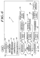
- FIG. 6 depicts a simplified flowchart 116 illustrating a method of performing image reproduction according to one embodiment of the invention.
- a scan operation begins with a scan request 118.
- an operator can issue a scan request by way of the user interface 44.
- the photoelectric array 26 scans a document on the platen 28 into the image data ASIC 74.
- the converter 38 and the input processor 40 (shown together as the scanner interface circuitry 120 in Figure 4) digitally convert and condition the image data.
- the optional compression network 104 compresses the image data according to well known algorithms.
- the memory controller ASIC 76 operating in master mode, reads the compressed image data from the read FIFO 100 via the PCI bus 78 and writes the compressed image data to the system memory 20 via the SCSI interface 80.
- the system controller 46 can respond to requests for additional processing from various sources, including the user interface 44 and the optional print controller 72.
- the media controller 88 retrieves the image data from the system memory 20.
- the read master controller 92 and the read buffer 86 operate in conjunction with the target decode and control logic 84 and the loopback master controller 110 to transfer the image data through the loopback FIFO 108 and the external interface logic 112 to the additional processing resources 85.
- the additional processing resources 85 perform additional processing on the image data, if desired.
- the memory controller ASIC 76 subsequent to performing the additional processing, retrieves the image data from the loopback FIFO 108 and returns the image data back to the system memory 20.
- the system controller 46 also responds to the presence of a user interface request from the touch screen display 56, the keyboard 58 and the mouse 60 of the user interface 44. If there is a request, the system controller 46 retrieves a copy of the image data from the system memory 20 and transfers that copy to the user interface 44 for display (steps 138 and 140). If there are no requests, the facility 15 then determines if there are any print requests.
- the system controller 46 can respond to print requests from, among other sources, the user interface 44. As indicated in steps 144 through 150 and as discussed in further detail with respect to Figure 3, in response to a print request, the system controller 46 retrieves a block of image data from the system memory 20 and transfers the image data directly to the image output controller 52. According to the illustrative embodiment, the image data is not intermediately stored in DRAM. The image output controller 52 decompresses and readies the image data for printing and forwards the print-ready image data to the printer stage 28. As specifically indicated at step 144 and as discussed in more detail with respect to Figure 5, the media controller 88 retrieves the data from the system memory 20 by way of the SCSI interface 80.
- the PCI controller 92 reads the image data from the read buffer 86 and transfers it using burst transfers directly to the write FIFO 94.
- the write master controller 96 signals the PCI controller 92 via the PCI bus 78 when the write FIFO 94 has sufficient free memory to accommodate a burst of data.
- the target decode and control circuitry 84 decodes the address of the write FIFO 94 from the PCI controller 92.
- the write FIFO 94 optionally, transfers the image data to be printed to the decompression network 98.
- the decompression circuitry 98 transfers the decompressed image data to the image output section 18 for printing.
- the media controller 88 purges the system memory 20 of the transferred image data.
- the illustrative flowchart 116 shows various steps occurring sequentially and in a particular order, the depicted steps can be rearranged and in some cases can occur concurrently, without departing from the essence of the invention.
- the steps involved in scanning an image into the system 10 can proceed concurrently with the steps involved in printing image data, previously stored in the system memory 20.
- an advantage of the illustrative system of the invention is that it does not require image data to be intermediately spooled between the system memory 20 and a DRAM page buffer.
- the memory controller ASIC 76 reads scanned image data in bursts over the PCI bus 78 and writes the bursts of image data to the system memory 20.
- the memory controller ASIC reads blocks of image data to the image output section 18 for image data from the system memory 20 and writes the blocks of image data to the image output section 18 for printing. According to the invention, no DRAM page buffer is necessary.
- the invention efficiently attains the objects set forth above, including reducing the amount of DRAM required to operate image reproduction systems and increasing the speed with which image data can be transferred by reducing the number of intermediate memory spooling operations.
Landscapes
- Engineering & Computer Science (AREA)
- Multimedia (AREA)
- Signal Processing (AREA)
- Computer Hardware Design (AREA)
- Microelectronics & Electronic Packaging (AREA)
- Facsimiles In General (AREA)
- Image Input (AREA)
- Storing Facsimile Image Data (AREA)
- Accessory Devices And Overall Control Thereof (AREA)
- Record Information Processing For Printing (AREA)
- Television Signal Processing For Recording (AREA)
Abstract
Description
Claims (20)
- An image data flow control and storage facility for operation in an image reproduction system, said facility comprisinga digital communication bus for transferring digital image data within said image reproduction system,a secondary storage device for storing digital image data within said image reproduction system,an image output controller in digital communication with said digital communication bus and adapted for receiving digital image data by way of said digital communication bus and for outputting said received digital image data,an image input controller in digital communication with said digital communication bus for transferring said digital image data to said facility by way of said digital communication bus, anda secondary storage controller in digital communication with said secondary storage device and said digital communication bus, and adapted for transferring at least one of digital image data directly from said secondary storage device to said image output controller, and digital image data directly from said image input controller to said secondary storage device, both by way of said digital communication bus.
- A facility according to claim 1, wherein said digital communication bus comprises a PCI-type bus.
- A facility according to claim 1 or claim 2, wherein said secondary storage controller is adapted for gaining control of said digital communication bus and for transferring blocks of digital image data over said bus in a burst format.
- A facility according to claim 3, wherein said secondary storage controller is adapted for operating in master mode to gain control of said digital communication bus and for transferring blocks of digital image data in a PCI-type burst format.
- A facility according to any of the preceding claims, wherein said secondary storage controller includes a buffer cache memory having a write buffer portion for accumulating a block of digital image data for direct transfer from said image input controller to said secondary storage device, and a read buffer portion for accumulating a block of digital image data for direct transfer from said secondary storage device to said image output controller.
- A facility according to claim 5, wherein said image output controller comprises an output cache memory for accumulating a block of digital image data for outputting, and said secondary storage controller includes a read master controller for determining whether said output cache memory has enough storage available to receive a block of digital image data and for writing a block of digital image data from said read buffer portion of said buffer cache memory directly to said output cache memory in response to determining that enough storage is available.
- A facility according to claim 6, wherein said read master controller comprises means for querying said image output controller to determine whether said output cache memory has enough storage available to receive a block of digital image data, and said image output controller includes output control elements in digital communication with said output cache memory and with said digital communication bus, wherein said output control elements, in response to a query from said read master controller, signal said read master controller regarding whether there is enough storage available in said output cache memory to receive a block of digital image data.
- A facility according to claim 7, wherein said output control elements are configured for generating a PCI-type disconnect signal for said read master controller when there is not enough storage available in said output cache memory to receive a block of digital image data.
- A facility according to any of claims 5 to 8, wherein said image input controller has an associated input cache memory for accumulating a block of digital image data for transfer to said write buffer portion of said buffer cache memory, and said secondary storage controller includes a write master controller for determining whether said input cache memory has accumulated a block of digital image data and for reading said block of digital image data directly from said input cache memory to said input buffer portion of said buffer cache memory in response to determining that a block of digital image data has been accumulated.
- A facility according to claim 9, wherein said write master controller is adapted for querying said image input controller to determine whether said input cache memory has accumulated a block of image data, and said image output controller includes input control elements in digital communication with said input cache memory and with said digital communication bus, wherein said input control elements, in response to a query from said PCI write master controller, signal said PCI write master controller regarding whether said input cache memory has accumulated a block of digital image data.
- A facility according to claim 10, wherein said input control elements signal a PCI-type disconnect, without transferring any image data to said PCI write master controller in response to said input cache memory not accumulating a block of digital image data.
- A facility according to any of claims 5 to 11, wherein said output cache memory and/or said input cache memory and/or said buffer cache memory comprises a FIFO-type cache memory.
- A facility according to any of the preceding claims, further comprising a loopback channel controller in digital communication with said digital communication bus and adapted for receiving digital image data by way of said digital communication bus and for outputting said received digital image data for additional processing, and said secondary storage controller is further adapted for transferring digital image data directly from said secondary storage device to said loop-back channel controller by way of said digital communication bus.
- A facility for operation in an image reproduction system having image data input and image data output interfaces, said facility comprisinga secondary storage device for storing image data within said image reproduction system,means for transferring said image data into said secondary storage device, without intermediately storing said digital image data in a DRAM buffer, andmeans for transferring digital image data, stored in said secondary storage device, to said image data output interface of said image reproduction system, without intermediately storing said digital image data in a DRAM buffer.
- A facility according to any of the preceding claims, wherein said secondary storage device comprises one of an optical storage device, a magnetic storage device, and a non-DRAM solid state storage device.
- A facility according to any of the preceding claims, further comprising an SCSI communication interface between said secondary storage device and said secondary storage controller.
- A method of transferring image data in an image reproduction system, said method comprising,transferring digital image data from an image input section of said image reproduction system directly to a secondary storage device, without intermediately storing said digital image data in a DRAM buffer, andtransferring said digital image data from said secondary storage device to an image output section of said image reproduction system, without intermediately storing said digital image data in a DRAM buffer.
- A method of transferring image data in an image reproduction system according to claim 17, wherein said method further comprisesproviding a digital communication bus for transferring said digital image data between said image input section and said secondary storage device, and between said image output section and said secondary storage device, andtransferring blocks of said digital image data from said image input section to said secondary storage device by way of said digital communication bus.
- A method of transferring image data in an image reproduction system according to claim 18, wherein said method further comprisestransferring blocks of said digital image data from said secondary storage device to said image output section by way of said digital communication bus.
- A method for transferring digital image data in an image reproduction system, said method comprisingproviding a digital communication bus for transferring digital image data within said image reproduction system,providing a secondary storage device for storing digital image data within said image reproduction system,providing an image output controller in digital communication with said digital communication bus and adapted for receiving digital image data by way of said digital communication bus and for outputting said received digital image data,providing an image input controller in digital communication with said digital communication bus for transferring said digital image data to said facility by way of said digital communication bus, andproviding a secondary storage controller in digital communication with said secondary storage device and said digital communication bus, and adapted for transferring at least one of digital image data directly from said secondary storage device to said image output controller, and digital image data directly from said image input controller to said secondary storage device, both by way of said digital communication bus.
Applications Claiming Priority (2)
| Application Number | Priority Date | Filing Date | Title |
|---|---|---|---|
| US360309 | 1990-12-18 | ||
| US09/360,309 US6496277B1 (en) | 1999-07-23 | 1999-07-23 | Data flow control and storage facility for an image reproduction system |
Publications (3)
| Publication Number | Publication Date |
|---|---|
| EP1071273A2 true EP1071273A2 (en) | 2001-01-24 |
| EP1071273A3 EP1071273A3 (en) | 2002-01-16 |
| EP1071273B1 EP1071273B1 (en) | 2008-02-27 |
Family
ID=23417460
Family Applications (1)
| Application Number | Title | Priority Date | Filing Date |
|---|---|---|---|
| EP00305810A Expired - Lifetime EP1071273B1 (en) | 1999-07-23 | 2000-07-10 | Data flow control and storage facility for an image reproduction system |
Country Status (4)
| Country | Link |
|---|---|
| US (1) | US6496277B1 (en) |
| EP (1) | EP1071273B1 (en) |
| JP (1) | JP2001069278A (en) |
| DE (1) | DE60038144T2 (en) |
Families Citing this family (14)
| Publication number | Priority date | Publication date | Assignee | Title |
|---|---|---|---|---|
| US20020063896A1 (en) * | 2000-11-29 | 2002-05-30 | Xerox Corporation | In an electronic reprographic system, provide automatic document integrity determination and page organization |
| KR100467102B1 (en) * | 2002-05-28 | 2005-01-24 | (주) 그레이프테크놀로지 | Data storage system |
| US7127568B2 (en) * | 2003-01-23 | 2006-10-24 | Hitachi, Ltd. | Throttling in storage systems |
| US7260677B1 (en) * | 2003-07-16 | 2007-08-21 | Unisys Corporation | Programmable system and method for accessing a shared memory |
| TWI233542B (en) * | 2003-07-18 | 2005-06-01 | Delta Electronics Inc | Auxiliary memory device for automation controller |
| KR101022472B1 (en) * | 2004-01-17 | 2011-03-16 | 삼성전자주식회사 | How to use the bus efficiently |
| JP2008017231A (en) * | 2006-07-06 | 2008-01-24 | Ricoh Co Ltd | Communication device |
| US8390877B2 (en) * | 2007-05-25 | 2013-03-05 | Xerox Corporation | Exportation of scanner's internal image auto-segmentation |
| US20130100334A1 (en) * | 2011-10-20 | 2013-04-25 | Broadcom Corporation | Method and System for an Adaptive Auto-Focus Algorithm |
| US10866897B2 (en) * | 2016-09-26 | 2020-12-15 | Samsung Electronics Co., Ltd. | Byte-addressable flash-based memory module with prefetch mode that is adjusted based on feedback from prefetch accuracy that is calculated by comparing first decoded address and second decoded address, where the first decoded address is sent to memory controller, and the second decoded address is sent to prefetch buffer |
| TWI773959B (en) * | 2019-01-31 | 2022-08-11 | 美商萬國商業機器公司 | Data processing system, method and computer program product for handling an input/output store instruction |
| CN113366438B (en) | 2019-01-31 | 2025-08-12 | 国际商业机器公司 | Processing I/O store instructions |
| JP7324282B2 (en) | 2019-01-31 | 2023-08-09 | インターナショナル・ビジネス・マシーンズ・コーポレーション | Methods, systems, and programs for handling input/output store instructions |
| JP2022096031A (en) * | 2020-12-17 | 2022-06-29 | ソニーセミコンダクタソリューションズ株式会社 | Image processor and method for processing image |
Family Cites Families (7)
| Publication number | Priority date | Publication date | Assignee | Title |
|---|---|---|---|---|
| US5303341A (en) | 1991-10-29 | 1994-04-12 | Xerox Corporation | Video processor for a printing apparatus |
| JPH07248992A (en) | 1994-03-10 | 1995-09-26 | Mita Ind Co Ltd | Image data transfer controller |
| US5581740A (en) | 1994-10-04 | 1996-12-03 | Dell Usa, L.P. | System for reading CD ROM data from hard disks |
| JPH09131931A (en) * | 1995-11-10 | 1997-05-20 | Brother Ind Ltd | Printer control device |
| US5963675A (en) | 1996-04-17 | 1999-10-05 | Sarnoff Corporation | Pipelined pyramid processor for image processing systems |
| JPH10254811A (en) | 1997-03-12 | 1998-09-25 | Sony Corp | Electronic device control apparatus and method |
| US6337746B1 (en) * | 1997-12-09 | 2002-01-08 | Jan R. Coyle | Interface card for coupling a computer to an external device |
-
1999
- 1999-07-23 US US09/360,309 patent/US6496277B1/en not_active Expired - Lifetime
-
2000
- 2000-07-10 DE DE60038144T patent/DE60038144T2/en not_active Expired - Lifetime
- 2000-07-10 EP EP00305810A patent/EP1071273B1/en not_active Expired - Lifetime
- 2000-07-13 JP JP2000212430A patent/JP2001069278A/en active Pending
Also Published As
| Publication number | Publication date |
|---|---|
| EP1071273B1 (en) | 2008-02-27 |
| EP1071273A3 (en) | 2002-01-16 |
| JP2001069278A (en) | 2001-03-16 |
| DE60038144T2 (en) | 2009-02-19 |
| US6496277B1 (en) | 2002-12-17 |
| DE60038144D1 (en) | 2008-04-10 |
Similar Documents
| Publication | Publication Date | Title |
|---|---|---|
| US7038795B2 (en) | Image input/output apparatus, method of controlling image input/output apparatus, image input/output system, and storage media | |
| US6362870B2 (en) | Image copier having enhanced duplex capabilities; method of printing a copy of a document to produce a duplex copy product | |
| US6529918B2 (en) | File system | |
| EP1071273B1 (en) | Data flow control and storage facility for an image reproduction system | |
| US6832010B2 (en) | Image processing apparatus | |
| US8243311B2 (en) | Image output apparatus for controlling order of print jobs and display jobs in queue | |
| US6285844B1 (en) | Image forming method and apparatus with automatic paper selection capability | |
| US5528374A (en) | Networked reproduction apparatus with security feature | |
| US6980702B2 (en) | Image processing apparatus | |
| JPH10285378A (en) | Copying device and control method therefor | |
| JPH11327857A (en) | Fault management system | |
| KR100505069B1 (en) | Portable storing medium and its recorder | |
| US5734482A (en) | Image processing apparatus and its control method | |
| JP3486478B2 (en) | Image forming apparatus and control method thereof | |
| US8427663B2 (en) | Image outputting apparatus holding output request for image data | |
| US7095525B2 (en) | Image processing apparatus and image processing method | |
| US5467181A (en) | Image forming system | |
| US7057762B1 (en) | Image processing method, image processing apparatus and image processing system | |
| US6504627B1 (en) | Image processing device | |
| US20030038998A1 (en) | Apparatus and method for scanning a copy job when a print path is not available | |
| JP2002019198A (en) | Image forming device | |
| US5402208A (en) | Image forming apparatus where vibrations of the scanner do not affect the write operation | |
| US6567185B1 (en) | Data acquisition and retrieval system for an image reproducing system | |
| JP3537108B2 (en) | Image processing system | |
| JPH0865425A (en) | Digital copier network system |
Legal Events
| Date | Code | Title | Description |
|---|---|---|---|
| PUAI | Public reference made under article 153(3) epc to a published international application that has entered the european phase |
Free format text: ORIGINAL CODE: 0009012 |
|
| AK | Designated contracting states |
Kind code of ref document: A2 Designated state(s): AT BE CH CY DE DK ES FI FR GB GR IE IT LI LU MC NL PT SE Kind code of ref document: A2 Designated state(s): DE FR GB |
|
| AX | Request for extension of the european patent |
Free format text: AL;LT;LV;MK;RO;SI |
|
| PUAL | Search report despatched |
Free format text: ORIGINAL CODE: 0009013 |
|
| AK | Designated contracting states |
Kind code of ref document: A3 Designated state(s): AT BE CH CY DE DK ES FI FR GB GR IE IT LI LU MC NL PT SE |
|
| AX | Request for extension of the european patent |
Free format text: AL;LT;LV;MK;RO;SI |
|
| 17P | Request for examination filed |
Effective date: 20020716 |
|
| AKX | Designation fees paid |
Free format text: DE FR GB |
|
| GRAP | Despatch of communication of intention to grant a patent |
Free format text: ORIGINAL CODE: EPIDOSNIGR1 |
|
| GRAS | Grant fee paid |
Free format text: ORIGINAL CODE: EPIDOSNIGR3 |
|
| GRAA | (expected) grant |
Free format text: ORIGINAL CODE: 0009210 |
|
| AK | Designated contracting states |
Kind code of ref document: B1 Designated state(s): DE FR GB |
|
| REG | Reference to a national code |
Ref country code: GB Ref legal event code: FG4D |
|
| REF | Corresponds to: |
Ref document number: 60038144 Country of ref document: DE Date of ref document: 20080410 Kind code of ref document: P |
|
| ET | Fr: translation filed | ||
| PLBE | No opposition filed within time limit |
Free format text: ORIGINAL CODE: 0009261 |
|
| STAA | Information on the status of an ep patent application or granted ep patent |
Free format text: STATUS: NO OPPOSITION FILED WITHIN TIME LIMIT |
|
| 26N | No opposition filed |
Effective date: 20081128 |
|
| REG | Reference to a national code |
Ref country code: FR Ref legal event code: PLFP Year of fee payment: 17 |
|
| PGFP | Annual fee paid to national office [announced via postgrant information from national office to epo] |
Ref country code: GB Payment date: 20160627 Year of fee payment: 17 |
|
| PGFP | Annual fee paid to national office [announced via postgrant information from national office to epo] |
Ref country code: FR Payment date: 20160622 Year of fee payment: 17 |
|
| PGFP | Annual fee paid to national office [announced via postgrant information from national office to epo] |
Ref country code: DE Payment date: 20160622 Year of fee payment: 17 |
|
| REG | Reference to a national code |
Ref country code: DE Ref legal event code: R119 Ref document number: 60038144 Country of ref document: DE |
|
| GBPC | Gb: european patent ceased through non-payment of renewal fee |
Effective date: 20170710 |
|
| REG | Reference to a national code |
Ref country code: FR Ref legal event code: ST Effective date: 20180330 |
|
| PG25 | Lapsed in a contracting state [announced via postgrant information from national office to epo] |
Ref country code: DE Free format text: LAPSE BECAUSE OF NON-PAYMENT OF DUE FEES Effective date: 20180201 Ref country code: GB Free format text: LAPSE BECAUSE OF NON-PAYMENT OF DUE FEES Effective date: 20170710 |
|
| PG25 | Lapsed in a contracting state [announced via postgrant information from national office to epo] |
Ref country code: FR Free format text: LAPSE BECAUSE OF NON-PAYMENT OF DUE FEES Effective date: 20170731 |