EP1071125A2 - Process for producing transistors having independently adjustable parameters - Google Patents
Process for producing transistors having independently adjustable parameters Download PDFInfo
- Publication number
- EP1071125A2 EP1071125A2 EP00114376A EP00114376A EP1071125A2 EP 1071125 A2 EP1071125 A2 EP 1071125A2 EP 00114376 A EP00114376 A EP 00114376A EP 00114376 A EP00114376 A EP 00114376A EP 1071125 A2 EP1071125 A2 EP 1071125A2
- Authority
- EP
- European Patent Office
- Prior art keywords
- gate structure
- doping
- base wafer
- sidewalls
- mosfet
- Prior art date
- Legal status (The legal status is an assumption and is not a legal conclusion. Google has not performed a legal analysis and makes no representation as to the accuracy of the status listed.)
- Withdrawn
Links
Images






Classifications
-
- H—ELECTRICITY
- H10—SEMICONDUCTOR DEVICES; ELECTRIC SOLID-STATE DEVICES NOT OTHERWISE PROVIDED FOR
- H10D—INORGANIC ELECTRIC SEMICONDUCTOR DEVICES
- H10D30/00—Field-effect transistors [FET]
-
- H—ELECTRICITY
- H10—SEMICONDUCTOR DEVICES; ELECTRIC SOLID-STATE DEVICES NOT OTHERWISE PROVIDED FOR
- H10W—GENERIC PACKAGES, INTERCONNECTIONS, CONNECTORS OR OTHER CONSTRUCTIONAL DETAILS OF DEVICES COVERED BY CLASS H10
- H10W20/00—Interconnections in chips, wafers or substrates
- H10W20/01—Manufacture or treatment
- H10W20/031—Manufacture or treatment of conductive parts of the interconnections
- H10W20/069—Manufacture or treatment of conductive parts of the interconnections by forming self-aligned vias or self-aligned contact plugs
-
- H—ELECTRICITY
- H10—SEMICONDUCTOR DEVICES; ELECTRIC SOLID-STATE DEVICES NOT OTHERWISE PROVIDED FOR
- H10D—INORGANIC ELECTRIC SEMICONDUCTOR DEVICES
- H10D30/00—Field-effect transistors [FET]
- H10D30/01—Manufacture or treatment
- H10D30/021—Manufacture or treatment of FETs having insulated gates [IGFET]
- H10D30/0217—Manufacture or treatment of FETs having insulated gates [IGFET] forming self-aligned punch-through stoppers or threshold implants under gate regions
-
- H—ELECTRICITY
- H10—SEMICONDUCTOR DEVICES; ELECTRIC SOLID-STATE DEVICES NOT OTHERWISE PROVIDED FOR
- H10D—INORGANIC ELECTRIC SEMICONDUCTOR DEVICES
- H10D30/00—Field-effect transistors [FET]
- H10D30/01—Manufacture or treatment
- H10D30/021—Manufacture or treatment of FETs having insulated gates [IGFET]
- H10D30/022—Manufacture or treatment of FETs having insulated gates [IGFET] having lightly-doped source or drain extensions selectively formed at the sides of the gates
-
- H—ELECTRICITY
- H10—SEMICONDUCTOR DEVICES; ELECTRIC SOLID-STATE DEVICES NOT OTHERWISE PROVIDED FOR
- H10D—INORGANIC ELECTRIC SEMICONDUCTOR DEVICES
- H10D30/00—Field-effect transistors [FET]
- H10D30/01—Manufacture or treatment
- H10D30/021—Manufacture or treatment of FETs having insulated gates [IGFET]
- H10D30/0223—Manufacture or treatment of FETs having insulated gates [IGFET] having source and drain regions or source and drain extensions self-aligned to sides of the gate
- H10D30/0225—Manufacture or treatment of FETs having insulated gates [IGFET] having source and drain regions or source and drain extensions self-aligned to sides of the gate using an initial gate mask complementary to the prospective gate location, e.g. using dummy source and drain electrodes
-
- H—ELECTRICITY
- H10—SEMICONDUCTOR DEVICES; ELECTRIC SOLID-STATE DEVICES NOT OTHERWISE PROVIDED FOR
- H10D—INORGANIC ELECTRIC SEMICONDUCTOR DEVICES
- H10D84/00—Integrated devices formed in or on semiconductor substrates that comprise only semiconducting layers, e.g. on Si wafers or on GaAs-on-Si wafers
- H10D84/01—Manufacture or treatment
- H10D84/0123—Integrating together multiple components covered by H10D12/00 or H10D30/00, e.g. integrating multiple IGBTs
- H10D84/0126—Integrating together multiple components covered by H10D12/00 or H10D30/00, e.g. integrating multiple IGBTs the components including insulated gates, e.g. IGFETs
- H10D84/0165—Integrating together multiple components covered by H10D12/00 or H10D30/00, e.g. integrating multiple IGBTs the components including insulated gates, e.g. IGFETs the components including complementary IGFETs, e.g. CMOS devices
- H10D84/0167—Manufacturing their channels
-
- H—ELECTRICITY
- H10—SEMICONDUCTOR DEVICES; ELECTRIC SOLID-STATE DEVICES NOT OTHERWISE PROVIDED FOR
- H10D—INORGANIC ELECTRIC SEMICONDUCTOR DEVICES
- H10D84/00—Integrated devices formed in or on semiconductor substrates that comprise only semiconducting layers, e.g. on Si wafers or on GaAs-on-Si wafers
- H10D84/01—Manufacture or treatment
- H10D84/02—Manufacture or treatment characterised by using material-based technologies
- H10D84/03—Manufacture or treatment characterised by using material-based technologies using Group IV technology, e.g. silicon technology or silicon-carbide [SiC] technology
- H10D84/038—Manufacture or treatment characterised by using material-based technologies using Group IV technology, e.g. silicon technology or silicon-carbide [SiC] technology using silicon technology, e.g. SiGe
-
- H—ELECTRICITY
- H10—SEMICONDUCTOR DEVICES; ELECTRIC SOLID-STATE DEVICES NOT OTHERWISE PROVIDED FOR
- H10W—GENERIC PACKAGES, INTERCONNECTIONS, CONNECTORS OR OTHER CONSTRUCTIONAL DETAILS OF DEVICES COVERED BY CLASS H10
- H10W20/00—Interconnections in chips, wafers or substrates
- H10W20/01—Manufacture or treatment
- H10W20/031—Manufacture or treatment of conductive parts of the interconnections
- H10W20/0698—Local interconnections
Definitions
- the present invention is generally directed to the manufacture of semiconductors and, more particularly, to the manufacture of MOSFET (metal oxide semiconductor field effect transistor) devices.
- MOSFET metal oxide semiconductor field effect transistor
- halo implant doping is often used to provide a region of enhanced channel doping at the perimeter of the source-drain (S-D) diffusions (e.g., boron halos are often used around the N+ S-D diffusions of NMOSFETs).
- S-D source-drain
- boron halos are often used around the N+ S-D diffusions of NMOSFETs.
- the need for high channel doping (including high halo implant doping) to suppress short channel roll-off can lead to increased junction leakage, high junction capacitance, and hot-carrier degradation.
- the increasing need for dual work-function gate conductors can lead to additional process integration complexity (in order to avoid boron penetration through the gate insulator).
- the primary object of the present invention is to provide an improved structure and process for producing semiconductor devices, such as MOSFET's, for purposes of reducing thermal budget and boron penetration concerns.
- Another object of the present invention is to reduce the aspect ratios which can be achieved, while maintaining a low sheet resistance.
- Still another object of the present invention is to provide an improved MOSFET channel structure which can implement such improvements.
- a still further object of the invention is to provide a MOSFET with improved electrical characteristics, including reduced short channel effect, lower junction capacitance, reduced junction leakage, and improved hot-carrier reliability.
- a novel structure and process for producing a MOSFET channel, lateral doping profile which suppresses short channel effects while providing low S-D junction capacitance and leakage, as well as immunity to hot-carrier effects.
- Yet another feature of the present invention is the potential for reduction in the contact stud-to-gate conductor capacitance, because the process of the present invention will allow a borderless contact to be formed with an oxide gate cap and oxide sidewall spacers.
- S-D junctions can be doped independently of the gate conductor doping which is performed.
- Such a process more easily allows the embodiment of N+ gated p-type field effect transistors (PFET's) and P+ gated n-type field effect transistors (NFET's), in addition to the standard N+ gated NFET's and P+ gated PFET's.
- PFET's N+ gated p-type field effect transistors
- NFET's P+ gated n-type field effect transistors
- the process and structures of the present invention achieve a variety of MOSFET structures. This flexibility is of significant value to product designers.
- a sacrificial oxide layer 1 is grown on a base wafer 2 (e.g., a silicon wafer), followed by the deposition of a layer 3 of polysilicon or an equivalent material and a layer 4 of silicon nitride (Si 3 N 4 ) or an equivalent material.
- the doping of the polysilicon layer 3 is not critical because this layer will later be used as an etch stop for the nitride etch.
- the thickness of the nitride layer 4 will determine the thickness of a low resistivity metal gate conductor layer (e.g., tungsten) which is subsequently to be formed.
- Raised shallow trench isolation (RSTI) regions 5 are then patterned and formed using processes which are themselves known in the industry. Before filling the RSTI regions 5, isolation implants are preferably performed, again using processes which are themselves known in the industry.
- the process continues by subjecting the nitride layer 4 and the RSTI region 5 to a directional anisotropic etching process selective to polysilicon, such as a reactive ion etching (RIE) process, through openings suitably patterned in a photoresist (PR) layer 7.
- RIE reactive ion etching
- PR photoresist
- the exposed polysilicon layer 3 is then subjected to a reactive ion etching process selective to nitride and oxide, stopping on the underlying sacrificial oxide layer 1.
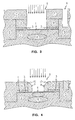
- Punch-through ion implantation (PT I/I) is illustrated by the arrows of Fig. 3.
- a relatively deep sub-surface, punch-through suppression implant 8 (a "stop pocket") is then formed to prevent punch through between the source and the drain of the MOSFET which is later to be formed.
- the photoresist layer 7 is then stripped and spacers 9 are formed on the sidewalls 10 of the openings 6.
- the spacers 9 are preferably formed of a material that contains a P-type dopant, for example, a glass such as BSG (borosilicate glass).
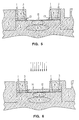
- the channel is then ion implanted (I/I) at low energy to set the threshold voltage (V t ) of the MOSFET, see the arrows of Fig. 4, defining the channel doping profile or V t implant 11.
- the edges of the V t implant 11 are offset from the sidewalls 10 of the polysilicon/nitride stack. As will be apparent from the description which follows, this type of profile results in low doping concentration adjacent to the S-D diffusion layers.
- the BSG spacers 9 are then stripped, selective to nitride layers 4 and to the fill of RSTI regions 5.
- the exposed sacrificial oxide layer 1 is thereafter stripped and a gate dielectric layer 12 is formed in its place.
- the gate dielectric layer 12 may be comprised of a thermally grown Si0 2 , a nitride gate oxide, or a deposited dielectric film.
- the gate dielectric layer 12 is also formed on the sidewalls 13 of the exposed polysilicon layer 3.
- a layer of polysilicon (or an equivalent material) is deposited to a thickness which completely fills the opening 6, to form a gate structure 14.
- the polysilicon layer is first planarized to the top surface of the pad nitride layers 4 and is then recessed selective to oxide and nitride, as shown. This polysilicon recessing operation substantially clears the wiring channel in the RSTI regions 5 of polysilicon.
- the exposed polysilicon of the gate structure 14 is then ion implanted, see the arrows of Fig. 6, to set the work-function of the gate conductor. This implant is preferably masked and performed twice to provided dual work-function gate doping.
- tungsten (or possibly another refractory metal such as tantalum or molybdenum, or the suicides of these refractory metals) is deposited over the gate structure 14, filling the cavity defined above the gate, and within the wiring channel 16 formed in the RSTI region 5.
- the tungsten layer 15 is planarized and recessed selective to oxide and nitride.
- a CVD (chemical vapor deposition) oxide layer 17 is then deposited and planarized to form an insulating cap over the tungsten layer 15.
- the tungsten forms a low-resistance gate and wiring layer.
- the oxide cap will later be used to form diffusion contacts which are borderless to the gate conductor. Referring to Fig.
- the pad nitride layer 4 is removed by etching with hot phosphoric acid (or an equivalent wet or dry etch which etches silicon nitride with a high selectivity to Si or SiO 2 ) and the exposed polysilicon layer 3 is subjected to an anisotropic etch (e.g., a reactive ion etch) selective to oxide.
- S-D extension implants 18 may be made at this point in the process, and supplemental halo implants may be added, if desired.
- Oxide spacers 19 are then formed on the sidewalls of the S-D contact openings and higher-concentration contact implants are made. It is important to note that the doping type for the S-D diffusion implantation is set independently of the doping type for the gate conductor.
- This flexibility allows a wide variety of MOSFET structures to be formed including P+ gated NFET's, N+ gated PFET's, N+ gated NFET's, and P+ gated PFET's.
- This feature gives the product designer added flexibility in selecting the threshold voltage (V t ) for the device being manufactured. Previously, significantly more complicated processes were required to provide such selection of the threshold voltage (V t ), because additional channel implants had to be made.
- P+ gated array NMOSFET devices allow a reduction in channel doping concentration (which improves data retention time), a reduced gate oxide field during wordline boost, and elimination of the need for "negative wordline low" because the negative gate potential is now achieved with a built-in work-function difference between the gate and the source.
- This "built-in negative wordline low” feature greatly simplifies the design of wordline drivers.
- the reduced doping distribution indicated in Fig. 8 provides a reduced electric field at the S-D junctions, which results in reduced junction capacitance, reduced leakage, and improved hot-carrier reliability.
- Borderless diffusion contacts to the gate conductors are used extensively in dynamic random access memory (DRAM) arrays, where density is of great importance.
- DRAM dynamic random access memory
- the foregoing process also allows borderless contacts to be used in MOSFET applications other than DRAM array transistors.
- a thin nitride layer 20 is first deposited over the structure shown in Fig. 8 so that the resulting deposit conforms to the underlying features.
- the nitride layer 20 provides an etch barrier over diffusions which are not desired to be contacted (e.g., storage node diffusion in a deep trench capacitor DRAM).
- the thin nitride layer 20 is opened at location 21, adjacent to the area where a borderless contact is desired. This opening step is preferably accomplished using an anisotropic (nitride spacer) etch which is selective to oxide. Etch selectivities of 8:1 are readily achieved using known methods.
- bitline halo implant may be performed to provide an extra degree of drain-induced barrier lowering (DIBL) protection without increasing junction leakage on the node diffusion side of an array MOSFET.
- DIBL drain-induced barrier lowering
- the bitline halo photoresist layer is then stripped.
- a polysilicon layer 22 is deposited and patterned to form landing pad regions for the metal studs which will provide contact to the higher-level metallurgy.
- a second embodiment is described with reference to the sequence of schematic illustrations shown in Figs. 10 to 15.
- This second embodiment provides a channel doping profile which differs from the profile of the MOSFET of the first embodiment.
- the MOSFET of the second embodiment has distinctly different electrical characteristics, which are important for meeting the needs of certain applications.
- Such special applications may include, for example, applications which require very low sensitivity of the threshold voltage (V t ) to variations in channel length, such as closely matched pairs of MOSFET's.
- the process of the second embodiment will be described from the point where it departs from the process of the first embodiment (i.e., following the process steps illustrated in Figs. 1 and 2).
- both the tailoring of the threshold voltage (V t ) and the punch-through (PT) stop implantation have been done, see the arrows of Fig. 10, before formation of the spacers 9.
- the PT implant was done before spacer formation and the V t implant followed the formation of the BSG spacer.
- the spacers 9 are formed on the sidewalls 10 of the exposed stack of polysilicon layer 3 and nitride layer 4.
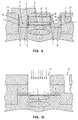
- a counterdoping implant 23 is made. See the arrows of Fig. 11.
- the counterdoping implant 23 is offset from the sidewalls 10 and is performed with a dopant species having a polarity which is opposite to the dopant species used for the preceding V t and PT implants to form stop pocket 8 and doping implant 11.
- the V t and PT implants would be performed with a P-type dopant such as boron or indium.
- the counterdoping implant 23 would then be performed with an N-type dopant such as arsenic or phosphorus.
- the V t doping implant 11 and the counterdoping implant 23 compensate each other to produce a doping concentration (in the embodiment illustrated, in the central region of the channel) which is less than the concentration produced by either the V t doping implant 11 or the counterdoping implant 23 alone.
- the net doping type in the counterdoped region may be either a P-type or an N-type, depending on the desired device characteristics. As in the first embodiment, and referring to Fig.
- V t doping pockets 11' are formed at the edges of the channel.
- the process then proceeds as described in the first embodiment with the formation of a polysilicon layer gate structure 14, and with the implantation of dual work-function dopants.
- this process step is then followed by the formation of the high-conductivity tungsten layer 15 for the gate stack and the wiring channel, and the formation of the cap oxide layers 17.
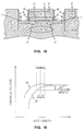
- the device of the second embodiment is shown following the previously described formation of the S-D extension implants 18 and the oxide spacers 19. Subsequent steps are then performed, as previously described for the first embodiment, to complete the desired structure.
- the principal difference between the device of the second embodiment and the device of the first embodiment deserves highlight.
- the former device has V t doping pockets 11' formed at the ends of the channel and light doping in the central region.
- the latter device has a single V t doping implant 11 formed as one pocket centered at the mid-channel and light doping at the ends of the channel.
- the V t roll-off characteristics 24 of the MOSFET of the second embodiment are qualitatively compared with the roll-off characteristics 25 of a standard MOSFET (i.e., a MOSFET having a conventional, uniform lateral doping distribution). Due to the presence of the (end) V t doping pockets 11', as the channel length of the MOSFET of the second embodiment is reduced, the threshold voltage (V t ) "bumps up” or remains fairly constant relative to the roll-off produced by the standard MOSFET. The degree of "bump-up" depends on the relative concentration of the V t doping pockets 11'.
- the doping pockets 11' extend over a larger percentage of the channel length.
- the V t doping concentration averaged over the length of the channel increases with decreasing channel length, compensating for the normal roll-off effect.
- RSTI raised shallow trench isolation
- STI shallow trench isolation
- the pad structure is preferably comprised of a sacrificial oxide layer 1 and a nitride layer 27 for use with STI regions 26. Distinguish this structure from the oxide/polysilicon/nitride system used with RSTI.
- the oxide/nitride pad structure used with the STI embodiment may be part of the pad structure originally formed on the substrate before conventional deep trench (DT) storage capacitor definition. As a result, for the STI process, the original pad structure need not be removed and a new pad structure need not be defined.
- This process is to be distinguished from the first two embodiments, using RSTI, where the oxide/polysilicon/nitride pad structure is preferably a new pad structure (because the oxide/polysilicon/nitride system is less compatible with a DT process).
- the STI process subjects the nitride layer 27 to a directional anisotropic etching process, such as an RIE process, through openings suitably patterned in a photoresist (PR) layer 7.
- a directional anisotropic etching process such as an RIE process
- PR photoresist
- apertures or openings 6 are concurrently formed in the (pad) nitride layer 27.
- Punch-through ion implantation PT I/I
- a relatively deep sub-surface, punch-through suppression implant 8 (a "stop pocket") is then formed to prevent punch through between the source and the drain of the MOSFET which is later to be formed.
- the photoresist layer 7 is then stripped and spacers 9 are formed on the sidewalls 10 of the opening 6.
- the spacers 9 are preferably formed of a material that contains a P-type dopant, for example, a glass such as BSG (borosilicate glass).
- the channel is then ion implanted (I/I) at low energy to set the threshold voltage (V t ) of the MOSFET, see the arrows of Fig. 19, defining the channel doping profile or V t implant 11.
- the edges of the V t implant 11 are offset from the sidewalls 10 of the polysilicon/nitride stack.
- the BSG spacers 9 are then stripped selective to nitride layers 27.
- the exposed sacrificial oxide layer 1 is thereafter stripped and a gate dielectric layer 12 is formed in its place.
- the gate dielectric layer 12 may be comprised of a thermally grown Si0 2 , a nitride gate oxide, or a deposited dielectric film.
- a layer of polysilicon (or an equivalent material) is deposited to a thickness which completely fills the opening 6, to form a gate structure 14.
- the polysilicon layer is first planarized to the top surface of the pad nitride layers 27 and is then recessed, as shown.
- the exposed polysilicon of the gate structure 14 is then ion implanted to set the work-function of the gate conductor (GC).
- GC gate conductor
- tungsten tantalum or molybdenum
- STI shallow trench isolation
- the STI embodiment because the height of the aperture 6 is lower than with raised STI (due to the absence of a poly layer), there is an increased probability that the top of the STI regions 26 will be recessed below the top surface of the silicon wafer 2. Such geometry, which results from the STI process, tends to degrade the ability to control the threshold voltage (V t ). It is considered desirable to have the top of the isolation elevated above the top of the silicon surface, which is ensured with the RSTI embodiments.
- the pad nitride layer 27 is removed by etching with hot phosphoric acid or an equivalent wet or dry etch which etches silicon nitride with a high selectivity to Si or SiO 2 .
- S-D extension implants 18 may be made at this point in the process, and supplemental halo implants may be added, if desired.
- Oxide spacers 19 are then formed on the sidewalls of the S-D contact openings and higher-concentration contact implants are made.
- CMOS complementary metal-oxide semiconductor
Landscapes
- Insulated Gate Type Field-Effect Transistor (AREA)
- Electrodes Of Semiconductors (AREA)
- Semiconductor Memories (AREA)
Abstract
Description
Referring to Fig. 5, the
Referring to Fig. 8, the pad nitride layer 4 is removed by etching with hot phosphoric acid (or an equivalent wet or dry etch which etches silicon nitride with a high selectivity to Si or SiO2) and the exposed
It is important to note that the doping type for the S-D diffusion implantation is set independently of the doping type for the gate conductor. This flexibility allows a wide variety of MOSFET structures to be formed including P+ gated NFET's, N+ gated PFET's, N+ gated NFET's, and P+ gated PFET's. This feature gives the product designer added flexibility in selecting the threshold voltage (Vt) for the device being manufactured. Previously, significantly more complicated processes were required to provide such selection of the threshold voltage (Vt), because additional channel implants had to be made.
As in the first embodiment, and referring to Fig. 12, the
Claims (74)
- A process for manufacturing a MOSFET structure, comprising the steps of:forming a layered structure including a sacrificial oxide layer covering a base wafer, a polysilicon layer covering the sacrificial oxide layer, and a nitride layer covering the polysilicon layer, wherein the layered structure is located between opposing raised shallow trench isolation regions;etching the nitride layer and the polysilicon layer to form an opening having sidewalls extending to the sacrificial oxide layer;forming spacers on the sidewalls of the opening;implanting the base wafer to set a threshold voltage for the MOSFET;stripping the spacers and the sacrificial oxide layer from the opening to expose the base wafer;forming a gate dielectric layer on the exposed base wafer; filling bottom portions of the opening with a doped gate structure;implanting the doped gate structure to set a work-function for the gate structure; andcovering the implanted gate structure with a refractory metal deposit.
- The process of claim 1 wherein the base wafer is formed of silicon.
- The process of claim 1 wherein the nitride layer is formed of Si3N4.
- The process of claim 1 wherein the etching of the nitride layer is performed with a directional anisotropic etching process which is selective to silicon, through openings patterned in a photoresist layer.
- The process of claim 4 wherein the directional anisotropic etching process is a reactive ion etching process.
- The process of claim 4 wherein the etching of the polysilicon layer is performed with a reactive ion etching process which is selective to nitride and oxide.
- The process of claim 1 further comprising the step of forming a sub-surface punch-through suppression implant in the base wafer, following the etching of the nitride layer and the polysilicon layer.
- The process of claim 1 wherein the spacers are formed of a material containing a P-type dopant.
- The process of claim 8 wherein the spacer material is borosilicate glass.
- The process of claim 1 further comprising the step of implanting the base wafer at low energy to set the threshold voltage.
- The process of claim 1 wherein the implanting of the base wafer to set the threshold voltage further includes the step of offsetting the implant from the sidewalls of the opening.
- The process of claim 11 wherein the offsetting produces a doping concentration adjacent to the sidewalls which is lower than a doping concentration produced toward center portions of the opening.
- The process of claim 1 further comprising the step of forming a counterdoping implant in the base wafer following the implanting of the base wafer to set the threshold voltage.
- The process of claim 13 wherein the implanting of the base wafer to set the threshold voltage is performed before the forming of the spacers on the sidewalls, and wherein the forming of the counterdoping implant is performed following the forming of the spacers on the sidewalls.
- The process of claim 13 wherein the forming of the counterdoping implant further includes the step of offsetting the counterdoping implant from the sidewalls of the opening.
- The process of claim 13 wherein the implanting of the base wafer to set the threshold voltage is performed with a doping species, and wherein the counterdoping implant is performed with a doping species which is opposite in polarity to the doping species for setting the threshold voltage.
- The process of claim 13 wherein the counterdoping implant and the implant for setting the threshold voltage combine to produce doping pockets adjacent to the sidewalls of the opening, developing a doping concentration adjacent to the sidewalls which is higher than a doping concentration produced toward center portions of the opening.
- The process of claim 1 wherein the gate dielectric is formed of a material selected from the group of dielectric materials including a thermally grown Si02, a nitride gate oxide, and a deposited dielectric film.
- The process of claim 1 wherein the filling of the bottom portions of the opening with the doped gate structure includes the steps of filling the opening with polysilicon, planarizing the polysilicon to top portions of the nitride layer, and recessing the planarized polysilicon to develop the gate structure.
- The process of claim 1 which further includes the steps of masking and performing the implanting of the doped gate structure twice, providing a dual work-function gate doping.
- The process of claim 1 wherein the refractory metal deposit is selected from the group of refractory materials including tungsten, tantalum, molybdenum, and the silicides of tungsten, tantalum, and molybdenum.
- The process of claim 1 which further includes the steps of recessing the gate structure and forming an insulating cap over the recessed gate structure.
- The process of claim 22 further comprising the steps of etching the nitride layer and the polysilicon layer remaining between the layered gate structure, refractory metal deposit and insulating cap, and the opposing raised shallow trench isolation regions, forming source/drain contact openings for the MOSFET.
- The process of claim 23 further comprising the steps of forming source/drain extension implants extending between the gate structure and the raised shallow trench isolation regions, and forming spacers on sidewalls of the source/drain contact openings.
- The process of claim 24 wherein the gate structure is set with a doping type, and wherein the source/drain extension implants are set with a doping type which is independent of the doping type set for the gate structure.
- The process of claim 24 further comprising the step of forming borderless contacts over the MOSFET structure.
- The process of claim 26 wherein the formation of the borderless contacts includes the steps of depositing a thin nitride layer over the MOSFET structure so that the nitride layer conforms to underlying features of the MOSFET structure, opening the thin nitride layer in an area for receiving a borderless contact, and depositing a polysilicon layer over the opened area and patterning the polysilicon layer to form a landing pad region for receiving a contact for the MOSFET.
- A process for manufacturing a MOSFET structure, comprising the steps of:forming a layered structure including a sacrificial oxide layer covering a base wafer and a nitride layer covering the sacrificial oxide layer, wherein the layered structure is located between opposing shallow trench isolation regions;etching the nitride layer to form an opening having sidewalls extending to the sacrificial oxide layer;forming spacers on the sidewalls of the opening;implanting the base wafer to set a threshold voltage for the MOSFET;stripping the spacers and the sacrificial oxide layer from the opening to expose the base wafer, and forming a gate dielectric layer on the exposed base wafer;filling bottom portions of the opening with a doped gate structure;implanting the doped gate structure to set a work-function for the gate structure; andcovering the implanted gate structure with a silicided deposit.
- The process of claim 28 wherein the base wafer is formed of silicon.
- The process of claim 28 wherein the nitride layer is formed of Si3N4.
- The process of claim 28 wherein the etching of the nitride layer is performed with a directional anisotropic etching process which is selective to silicon, through openings patterned in a photoresist layer.
- The process of claim 31 wherein the directional anisotropic etching process is a reactive ion etching process.
- The process of claim 28 further comprising the step of forming a sub-surface punch-through suppression implant in the base wafer, following the etching of the nitride layer.
- The process of claim 28 wherein the spacers are formed of a material containing a P-type dopant.
- The process of claim 34 wherein the spacer material is borosilicate glass.
- The process of claim 28 further comprising the step of implanting the base wafer at low energy to set the threshold voltage.
- The process of claim 28 wherein the implanting of the base wafer to set the threshold voltage further includes the step of offsetting the implant from the sidewalls of the opening.
- The process of claim 37 wherein the offsetting produces a doping concentration adjacent to the sidewalls which is lower than a doping concentration produced toward center portions of the opening.
- The process of claim 28 which further includes the step of forming a counterdoping implant in the base wafer following the implanting of the base wafer to set the threshold voltage.
- The process of claim 39 wherein the implanting of the base wafer to set the threshold voltage is performed before the forming of the spacers on the sidewalls, and wherein the forming of the counterdoping implant is performed following the forming of the spacers on the sidewalls.
- The process of claim 39 wherein the forming of the counterdoping implant further includes the step of offsetting the counterdoping implant from the sidewalls of the opening.
- The process of claim 39 wherein the implanting of the base wafer to set the threshold voltage is performed with a doping species, and wherein the counterdoping implant is performed with a doping species which is opposite in polarity to the doping species for setting the threshold voltage.
- The process of claim 39 wherein the counterdoping implant and the implant for setting the threshold voltage combine to produce doping pockets adjacent to the sidewalls of the opening, developing a doping concentration adjacent to the sidewalls which is higher than a doping concentration produced toward center portions of the opening.
- The process of claim 28 wherein the gate dielectric is formed of a material selected from the group of dielectric materials including a thermally grown Si02, a nitride gate oxide, and a deposited dielectric film.
- The process of claim 28 wherein the filling of the bottom portions of the opening with the doped gate structure includes the steps of filling the opening with polysilicon, planarizing the polysilicon to top portions of the nitride layer, and recessing the planarized polysilicon to develop the gate structure.
- The process of claim 28 which further includes the steps of masking and performing the implanting of the doped gate structure twice, providing a dual work-function gate doping.
- The process of claim 28 wherein the silicide deposit is selected from the group of materials including silicides of tungsten, tantalum, and molybdenum.
- The process of claim 28 which further includes the step of etching the nitride layer remaining adjacent to the layered gate structure and the silicide deposit.
- The process of claim 48 which further includes the steps of forming source/drain extension implants extending between the layered gate structure and the shallow trench isolation regions, and forming spacers on sidewalls of the layered gate structure.
- The process of claim 49 wherein the gate structure is set with a doping type, and wherein the source/drain extension implants are set with a doping type which is independent of the doping type set for the gate structure.
- A MOSFET structure comprising:a layered gate structure including a base wafer, a gate dielectric layer covering the base wafer, a doped gate structure covering the gate dielectric layer and being implanted to set a work-function for the gate structure, a refractory metal deposit covering the doped gate structure, and an oxide cap covering the refractory metal deposit; raised shallow trench isolation regions spaced from and located on opposing sides of the layered gate structure, developing open channels between the layered gate structure and the raised shallow trench isolation regions;source/drain extension implants electrically connecting and extending between the layered gate structure and the raised shallow trench isolation regions;an implanted punch-through stop pocket formed in the base wafer and positioned beneath the layered gate structure; andan implant setting a threshold voltage for the MOSFET structure, formed in the base wafer and positioned beneath the layered gate structure, and located between the implanted punch-through stop pocket and the layered gate structure.
- The structure of claim 51 wherein the base wafer is formed of silicon.
- The structure of claim 51 wherein the implant setting the threshold voltage is offset from the sidewalls of the layered gate structure.
- The structure of claim 53 wherein the offset produces a doping concentration adjacent to the sidewalls which is lower than a doping concentration produced toward center portions of the layered gate structure.
- The structure of claim 51 having a plurality of doping pockets for determining the threshold voltage, wherein the doping pockets are positioned adjacent to and offset from the sidewalls of the layered gate structure.
- The structure of claim 55 wherein the doping pockets are positioned to produce a doping concentration adjacent to the sidewalls which is higher than a doping concentration produced toward center portions of the layered gate structure.
- The structure of claim 51 wherein the gate dielectric layer is formed of a material selected from the group of dielectric materials including a thermally grown Si02, a nitride gate oxide, and a deposited dielectric film.
- The structure of claim 51 wherein the doped gate structure incorporates dual work-function gate doping.
- The structure of claim 51 wherein the refractory metal deposit is selected from the group of refractory materials including tungsten, tantalum, molybdenum, and the silicides of tungsten, tantalum, and molybdenum.
- The structure of claim 51 wherein the gate structure is set with a doping type, and wherein the source/drain extension implants are set with a doping type which is independent of the doping type set for the gate structure.
- The structure of claim 51 further comprising a borderless contact formed over the MOSFET structure.
- The structure of claim 61 wherein the borderless contact includes a thin nitride layer deposited over the MOSFET structure so that the nitride layer conforms to underlying features of the MOSFET structure, an opening formed in the thin nitride layer in an area for receiving the borderless contact, and a polysilicon layer deposited over the opened area and patterned to form a landing pad region for receiving a contact for the MOSFET.
- The structure of claim 51 wherein the MOSFET structure defines a gated array MOSFET.
- A MOSFET structure comprising:a layered gate structure including a base wafer, a gate dielectric layer covering the base wafer, a doped gate structure covering the gate dielectric layer and being implanted to set a work-function for the gate structure, and a refractory metal deposit covering the doped gate structure;shallow trench isolation regions spaced from and located on opposing sides of the layered gate structure;source/drain extension implants electrically connecting and extending between the layered gate structure and the shallow trench isolation regions;an implanted punch-through stop pocket formed in the base wafer and positioned beneath the layered gate structure; andan implant setting a threshold voltage for the MOSFET structure, formed in the base wafer and positioned beneath the layered gate structure, and located between the implanted punch-through stop pocket and the layered gate structure.
- The structure of claim 64 wherein the base wafer is formed of silicon.
- The structure of claim 64 wherein the implant for setting the threshold voltage is offset from the sidewalls of the layered gate structure.
- The structure of claim 66 wherein the offset produces a doping concentration adjacent to the sidewalls which is lower than a doping concentration produced toward center portions of the layered gate structure.
- The structure of claim 64 having a plurality of doping pockets for determining the threshold voltage, wherein the doping pockets are positioned adjacent to and offset from the sidewalls of the layered gate structure.
- The structure of claim 68 wherein the doping pockets are positioned to produce a doping concentration adjacent to the sidewalls which is higher than a doping concentration produced toward center portions of the layered gate structure.
- The structure of claim 64 wherein the gate dielectric layer is formed of a material selected from the group of dielectric materials including a thermally grown Si02, a nitride gate oxide, and a deposited dielectric film.
- The structure of claim 64 wherein the doped gate structure incorporates dual work-function gate doping.
- The structure of claim 64 wherein the silicide deposit is selected from the group of materials including suicides of tungsten, tantalum, and molybdenum.
- The structure of claim 64 wherein the gate structure is set with a doping type, and wherein the source/drain extension implants are set with a doping type which is independent of the doping type set for the gate structure.
- The structure of claim 64 wherein the MOSFET structure defines a gated array MOSFET.
Applications Claiming Priority (2)
| Application Number | Priority Date | Filing Date | Title |
|---|---|---|---|
| US359291 | 1999-07-22 | ||
| US09/359,291 US6501131B1 (en) | 1999-07-22 | 1999-07-22 | Transistors having independently adjustable parameters |
Publications (2)
| Publication Number | Publication Date |
|---|---|
| EP1071125A2 true EP1071125A2 (en) | 2001-01-24 |
| EP1071125A3 EP1071125A3 (en) | 2005-06-01 |
Family
ID=23413192
Family Applications (1)
| Application Number | Title | Priority Date | Filing Date |
|---|---|---|---|
| EP00114376A Withdrawn EP1071125A3 (en) | 1999-07-22 | 2000-07-05 | Process for producing transistors having independently adjustable parameters |
Country Status (6)
| Country | Link |
|---|---|
| US (1) | US6501131B1 (en) |
| EP (1) | EP1071125A3 (en) |
| JP (1) | JP3516442B2 (en) |
| KR (1) | KR100661399B1 (en) |
| CN (1) | CN1148791C (en) |
| TW (1) | TW516232B (en) |
Cited By (2)
| Publication number | Priority date | Publication date | Assignee | Title |
|---|---|---|---|---|
| US6319817B1 (en) * | 1995-10-23 | 2001-11-20 | Sony Corporation | Method of forming viahole |
| DE102008059648A1 (en) * | 2008-11-28 | 2010-06-02 | Advanced Micro Devices, Inc., Sunnyvale | Greater ε gate electrode structure formed after transistor fabrication using a spacer |
Families Citing this family (55)
| Publication number | Priority date | Publication date | Assignee | Title |
|---|---|---|---|---|
| DE10027397A1 (en) * | 2000-06-02 | 2001-12-13 | Graffinity Pharm Design Gmbh | Surface for the immobilization of ligands |
| JP2002033477A (en) * | 2000-07-13 | 2002-01-31 | Nec Corp | Semiconductor device and method of manufacturing the same |
| JP2002100746A (en) * | 2000-09-21 | 2002-04-05 | Hitachi Ltd | Semiconductor integrated circuit device and method of manufacturing the same |
| KR100713905B1 (en) * | 2001-06-29 | 2007-05-07 | 주식회사 하이닉스반도체 | Manufacturing method of semiconductor device |
| KR20030041193A (en) * | 2001-11-19 | 2003-05-27 | 삼성전자주식회사 | Method for fabricating transistor of semiconductor device |
| DE10232938B4 (en) * | 2002-07-19 | 2005-05-04 | Infineon Technologies Ag | Method for producing a buried bit line for a semiconductor memory |
| US7825488B2 (en) | 2006-05-31 | 2010-11-02 | Advanced Analogic Technologies, Inc. | Isolation structures for integrated circuits and modular methods of forming the same |
| US6900091B2 (en) * | 2002-08-14 | 2005-05-31 | Advanced Analogic Technologies, Inc. | Isolated complementary MOS devices in epi-less substrate |
| US6855985B2 (en) | 2002-09-29 | 2005-02-15 | Advanced Analogic Technologies, Inc. | Modular bipolar-CMOS-DMOS analog integrated circuit & power transistor technology |
| US6887758B2 (en) * | 2002-10-09 | 2005-05-03 | Freescale Semiconductor, Inc. | Non-volatile memory device and method for forming |
| KR100485176B1 (en) * | 2003-01-30 | 2005-04-22 | 동부아남반도체 주식회사 | Fabrication method of MOS transistor |
| US20040256679A1 (en) * | 2003-06-17 | 2004-12-23 | Hu Yongjun J. | Dual work function metal gates and method of forming |
| US6909151B2 (en) | 2003-06-27 | 2005-06-21 | Intel Corporation | Nonplanar device with stress incorporation layer and method of fabrication |
| US7456476B2 (en) | 2003-06-27 | 2008-11-25 | Intel Corporation | Nonplanar semiconductor device with partially or fully wrapped around gate electrode and methods of fabrication |
| US7060546B2 (en) * | 2003-11-26 | 2006-06-13 | International Business Machines Corporation | Ultra-thin SOI MOSFET method and structure |
| US7056794B2 (en) * | 2004-01-09 | 2006-06-06 | International Business Machines Corporation | FET gate structure with metal gate electrode and silicide contact |
| US6974736B2 (en) * | 2004-01-09 | 2005-12-13 | International Business Machines Corporation | Method of forming FET silicide gate structures incorporating inner spacers |
| US20050191812A1 (en) * | 2004-03-01 | 2005-09-01 | Lsi Logic Corporation | Spacer-less transistor integration scheme for high-k gate dielectrics and small gate-to-gate spaces applicable to Si, SiGe strained silicon schemes |
| US7154118B2 (en) | 2004-03-31 | 2006-12-26 | Intel Corporation | Bulk non-planar transistor having strained enhanced mobility and methods of fabrication |
| KR100615593B1 (en) * | 2004-05-06 | 2006-08-25 | 주식회사 하이닉스반도체 | Method for manufacturing a semiconductor device having a recess channel |
| US7579280B2 (en) | 2004-06-01 | 2009-08-25 | Intel Corporation | Method of patterning a film |
| US7042009B2 (en) | 2004-06-30 | 2006-05-09 | Intel Corporation | High mobility tri-gate devices and methods of fabrication |
| US7348284B2 (en) | 2004-08-10 | 2008-03-25 | Intel Corporation | Non-planar pMOS structure with a strained channel region and an integrated strained CMOS flow |
| US7422946B2 (en) | 2004-09-29 | 2008-09-09 | Intel Corporation | Independently accessed double-gate and tri-gate transistors in same process flow |
| US7361958B2 (en) | 2004-09-30 | 2008-04-22 | Intel Corporation | Nonplanar transistors with metal gate electrodes |
| US20060086977A1 (en) | 2004-10-25 | 2006-04-27 | Uday Shah | Nonplanar device with thinned lower body portion and method of fabrication |
| US7675094B2 (en) | 2004-12-22 | 2010-03-09 | Omnivision Technologies, Inc. | Image sensor pixel having a transfer gate formed from P+ or N+ doped polysilicon |
| US7518196B2 (en) | 2005-02-23 | 2009-04-14 | Intel Corporation | Field effect transistor with narrow bandgap source and drain regions and method of fabrication |
| KR100712989B1 (en) * | 2005-03-14 | 2007-05-02 | 주식회사 하이닉스반도체 | Manufacturing method of semiconductor device having recess channel and asymmetric junction structure |
| US20060202266A1 (en) | 2005-03-14 | 2006-09-14 | Marko Radosavljevic | Field effect transistor with metal source/drain regions |
| US7858481B2 (en) | 2005-06-15 | 2010-12-28 | Intel Corporation | Method for fabricating transistor with thinned channel |
| US7547637B2 (en) | 2005-06-21 | 2009-06-16 | Intel Corporation | Methods for patterning a semiconductor film |
| US7279375B2 (en) | 2005-06-30 | 2007-10-09 | Intel Corporation | Block contact architectures for nanoscale channel transistors |
| US7402875B2 (en) | 2005-08-17 | 2008-07-22 | Intel Corporation | Lateral undercut of metal gate in SOI device |
| WO2007023979A1 (en) * | 2005-08-22 | 2007-03-01 | Nec Corporation | Mosfet and production memthod of semiconductor device |
| US7479421B2 (en) | 2005-09-28 | 2009-01-20 | Intel Corporation | Process for integrating planar and non-planar CMOS transistors on a bulk substrate and article made thereby |
| US20070090416A1 (en) | 2005-09-28 | 2007-04-26 | Doyle Brian S | CMOS devices with a single work function gate electrode and method of fabrication |
| US7381610B2 (en) * | 2005-11-04 | 2008-06-03 | International Business Machines Corporation | Semiconductor transistors with contact holes close to gates |
| US7485503B2 (en) | 2005-11-30 | 2009-02-03 | Intel Corporation | Dielectric interface for group III-V semiconductor device |
| US7679146B2 (en) * | 2006-05-30 | 2010-03-16 | Semiconductor Components Industries, Llc | Semiconductor device having sub-surface trench charge compensation regions |
| US8143646B2 (en) | 2006-08-02 | 2012-03-27 | Intel Corporation | Stacking fault and twin blocking barrier for integrating III-V on Si |
| US8362566B2 (en) | 2008-06-23 | 2013-01-29 | Intel Corporation | Stress in trigate devices using complimentary gate fill materials |
| US7964922B2 (en) * | 2008-08-15 | 2011-06-21 | International Business Machines Corporation | Structure, design structure and method of manufacturing dual metal gate VT roll-up structure |
| US8003463B2 (en) * | 2008-08-15 | 2011-08-23 | International Business Machines Corporation | Structure, design structure and method of manufacturing dual metal gate Vt roll-up structure |
| CN101728264B (en) * | 2008-10-24 | 2011-10-05 | 中芯国际集成电路制造(上海)有限公司 | Method for controlling source/drain junction capacitance and method for forming PMOS transistor |
| US8421162B2 (en) | 2009-09-30 | 2013-04-16 | Suvolta, Inc. | Advanced transistors with punch through suppression |
| US8273617B2 (en) | 2009-09-30 | 2012-09-25 | Suvolta, Inc. | Electronic devices and systems, and methods for making and using the same |
| US8530971B2 (en) | 2009-11-12 | 2013-09-10 | International Business Machines Corporation | Borderless contacts for semiconductor devices |
| US8759872B2 (en) | 2010-06-22 | 2014-06-24 | Suvolta, Inc. | Transistor with threshold voltage set notch and method of fabrication thereof |
| US8546219B2 (en) | 2011-10-13 | 2013-10-01 | International Business Machines Corporation | Reducing performance variation of narrow channel devices |
| US8900954B2 (en) | 2011-11-04 | 2014-12-02 | International Business Machines Corporation | Blanket short channel roll-up implant with non-angled long channel compensating implant through patterned opening |
| US8835265B1 (en) * | 2012-06-18 | 2014-09-16 | Altera Corporation | High-k dielectric device and process |
| CN104347707B (en) * | 2013-08-06 | 2018-01-30 | 中国科学院微电子研究所 | A kind of MOSFET structure and its manufacturing method |
| CN105576026B (en) * | 2014-10-16 | 2018-11-16 | 中芯国际集成电路制造(上海)有限公司 | Semiconductor devices and preparation method thereof |
| US9972694B2 (en) * | 2015-10-20 | 2018-05-15 | Taiwan Semiconductor Manufacturing Company, Ltd. | Atomic layer deposition methods and structures thereof |
Family Cites Families (21)
| Publication number | Priority date | Publication date | Assignee | Title |
|---|---|---|---|---|
| US4745079A (en) * | 1987-03-30 | 1988-05-17 | Motorola, Inc. | Method for fabricating MOS transistors having gates with different work functions |
| US5244823A (en) * | 1991-05-21 | 1993-09-14 | Sharp Kabushiki Kaisha | Process for fabricating a semiconductor device |
| US5571738A (en) * | 1992-09-21 | 1996-11-05 | Advanced Micro Devices, Inc. | Method of making poly LDD self-aligned channel transistors |
| US5270234A (en) * | 1992-10-30 | 1993-12-14 | International Business Machines Corporation | Deep submicron transistor fabrication method |
| KR960008735B1 (en) * | 1993-04-29 | 1996-06-29 | Samsung Electronics Co Ltd | Mos transistor and the manufacturing method thereof |
| US5413949A (en) * | 1994-04-26 | 1995-05-09 | United Microelectronics Corporation | Method of making self-aligned MOSFET |
| US5434093A (en) * | 1994-08-10 | 1995-07-18 | Intel Corporation | Inverted spacer transistor |
| JP2586342B2 (en) * | 1994-08-27 | 1997-02-26 | 日本電気株式会社 | Method for manufacturing semiconductor device |
| US5605855A (en) * | 1995-02-28 | 1997-02-25 | Motorola Inc. | Process for fabricating a graded-channel MOS device |
| KR0161398B1 (en) * | 1995-03-13 | 1998-12-01 | 김광호 | High breakdown voltage transistor and manufacturing method thereof |
| US5688700A (en) * | 1995-11-03 | 1997-11-18 | Micron Technology, Inc. | Method of forming a field effect transistor |
| US5614430A (en) * | 1996-03-11 | 1997-03-25 | Taiwan Semiconductor Manufacturing Company Ltd. | Anti-punchthrough ion implantation for sub-half micron channel length MOSFET devices |
| US5849621A (en) * | 1996-06-19 | 1998-12-15 | Advanced Micro Devices, Inc. | Method and structure for isolating semiconductor devices after transistor formation |
| US5915181A (en) * | 1996-07-22 | 1999-06-22 | Vanguard International Semiconductor Corporation | Method for forming a deep submicron MOSFET device using a silicidation process |
| US5804496A (en) * | 1997-01-08 | 1998-09-08 | Advanced Micro Devices | Semiconductor device having reduced overlap capacitance and method of manufacture thereof |
| US5899719A (en) * | 1997-02-14 | 1999-05-04 | United Semiconductor Corporation | Sub-micron MOSFET |
| US5879998A (en) * | 1997-07-09 | 1999-03-09 | Advanced Micro Devices, Inc. | Adaptively controlled, self-aligned, short channel device and method for manufacturing same |
| US5776821A (en) * | 1997-08-22 | 1998-07-07 | Vlsi Technology, Inc. | Method for forming a reduced width gate electrode |
| US5856225A (en) * | 1997-11-24 | 1999-01-05 | Chartered Semiconductor Manufacturing Ltd | Creation of a self-aligned, ion implanted channel region, after source and drain formation |
| TW364207B (en) * | 1997-12-20 | 1999-07-11 | United Microelectronics Corp | Method for producing DRAM |
| US5888867A (en) * | 1998-02-13 | 1999-03-30 | Advanced Micro Devices, Inc. | Non-uniform threshold voltage adjustment in flash eproms through gate work function alteration |
-
1999
- 1999-07-22 US US09/359,291 patent/US6501131B1/en not_active Expired - Lifetime
-
2000
- 2000-04-13 TW TW089106874A patent/TW516232B/en not_active IP Right Cessation
- 2000-07-05 EP EP00114376A patent/EP1071125A3/en not_active Withdrawn
- 2000-07-11 JP JP2000210075A patent/JP3516442B2/en not_active Expired - Fee Related
- 2000-07-12 CN CNB00120498XA patent/CN1148791C/en not_active Expired - Fee Related
- 2000-07-20 KR KR1020000041581A patent/KR100661399B1/en not_active Expired - Fee Related
Cited By (5)
| Publication number | Priority date | Publication date | Assignee | Title |
|---|---|---|---|---|
| US6319817B1 (en) * | 1995-10-23 | 2001-11-20 | Sony Corporation | Method of forming viahole |
| DE102008059648A1 (en) * | 2008-11-28 | 2010-06-02 | Advanced Micro Devices, Inc., Sunnyvale | Greater ε gate electrode structure formed after transistor fabrication using a spacer |
| DE102008059648B4 (en) * | 2008-11-28 | 2011-12-22 | Advanced Micro Devices, Inc. | Greater ε gate electrode structure formed after transistor fabrication using a spacer |
| US8470661B2 (en) | 2008-11-28 | 2013-06-25 | Advanced Micro Devices, Inc. | High-K gate electrode structure formed after transistor fabrication by using a spacer |
| US8883582B2 (en) | 2008-11-28 | 2014-11-11 | Advanced Micro Devices, Inc. | High-K gate electrode structure formed after transistor fabrication by using a spacer |
Also Published As
| Publication number | Publication date |
|---|---|
| JP3516442B2 (en) | 2004-04-05 |
| KR100661399B1 (en) | 2006-12-27 |
| CN1148791C (en) | 2004-05-05 |
| US6501131B1 (en) | 2002-12-31 |
| EP1071125A3 (en) | 2005-06-01 |
| HK1032293A1 (en) | 2001-07-13 |
| JP2001068672A (en) | 2001-03-16 |
| KR20010039731A (en) | 2001-05-15 |
| CN1286495A (en) | 2001-03-07 |
| TW516232B (en) | 2003-01-01 |
Similar Documents
| Publication | Publication Date | Title |
|---|---|---|
| US6501131B1 (en) | Transistors having independently adjustable parameters | |
| US6403423B1 (en) | Modified gate processing for optimized definition of array and logic devices on same chip | |
| US6281064B1 (en) | Method for providing dual work function doping and protective insulating cap | |
| US5539229A (en) | MOSFET with raised STI isolation self-aligned to the gate stack | |
| US6337262B1 (en) | Self aligned T-top gate process integration | |
| EP0862208A2 (en) | Semiconductor device and method of manufacturing the same | |
| JPH11274496A (en) | FIELD EFFECT TRANSISTOR HAVING IMPROVED IMPLANT AND METHOD OF MANUFACTURING THE SAME | |
| US7009255B2 (en) | Semiconductor device having punch-through structure off-setting the edge of the gate electrodes | |
| US6177336B1 (en) | Method for fabricating a metal-oxide semiconductor device | |
| US6943084B2 (en) | Semiconductor device on silicon-on-insulator and method for manufacturing the semiconductor device | |
| US6586296B1 (en) | Method of doping wells, channels, and gates of dual gate CMOS technology with reduced number of masks | |
| US6355531B1 (en) | Method for fabricating semiconductor devices with different properties using maskless process | |
| US6333220B1 (en) | Method and apparatus for providing low-GIDL dual workfunction gate doping with borderless diffusion contact | |
| US6528371B2 (en) | Method for fabricating semiconductor device | |
| US6313006B1 (en) | Method of field implantation | |
| JP2003037185A (en) | Method for manufacturing semiconductor device | |
| KR20040057535A (en) | Method of manufacturing a semiconductor device | |
| HK1032293B (en) | Structure and process integration for producing transistors having independently adjustable parameters |
Legal Events
| Date | Code | Title | Description |
|---|---|---|---|
| PUAI | Public reference made under article 153(3) epc to a published international application that has entered the european phase |
Free format text: ORIGINAL CODE: 0009012 |
|
| AK | Designated contracting states |
Kind code of ref document: A2 Designated state(s): AT BE CH CY DE DK ES FI FR GB GR IE IT LI LU MC NL PT SE |
|
| AX | Request for extension of the european patent |
Free format text: AL;LT;LV;MK;RO;SI |
|
| RIN1 | Information on inventor provided before grant (corrected) |
Inventor name: RENGARAJAN, RAJESH Inventor name: MANDELMAN, JACK Inventor name: GAMBINO, JEFFREY P. Inventor name: DIVAKARUNI, RAMA |
|
| PUAL | Search report despatched |
Free format text: ORIGINAL CODE: 0009013 |
|
| AK | Designated contracting states |
Kind code of ref document: A3 Designated state(s): AT BE CH CY DE DK ES FI FR GB GR IE IT LI LU MC NL PT SE |
|
| AX | Request for extension of the european patent |
Extension state: AL LT LV MK RO SI |
|
| 17P | Request for examination filed |
Effective date: 20050930 |
|
| AKX | Designation fees paid |
Designated state(s): AT BE CH CY DE DK ES FI FR GB GR IE IT LI LU MC NL PT SE |
|
| 17Q | First examination report despatched |
Effective date: 20070716 |
|
| RAP1 | Party data changed (applicant data changed or rights of an application transferred) |
Owner name: QIMONDA AG Owner name: INTERNATIONAL BUSINESS MACHINES CORPORATION |
|
| STAA | Information on the status of an ep patent application or granted ep patent |
Free format text: STATUS: THE APPLICATION IS DEEMED TO BE WITHDRAWN |
|
| 18D | Application deemed to be withdrawn |
Effective date: 20080701 |