EP1069614A2 - Method of fabricating an integrated circuit - Google Patents
Method of fabricating an integrated circuit Download PDFInfo
- Publication number
- EP1069614A2 EP1069614A2 EP00305834A EP00305834A EP1069614A2 EP 1069614 A2 EP1069614 A2 EP 1069614A2 EP 00305834 A EP00305834 A EP 00305834A EP 00305834 A EP00305834 A EP 00305834A EP 1069614 A2 EP1069614 A2 EP 1069614A2
- Authority
- EP
- European Patent Office
- Prior art keywords
- plasma etcher
- polycrystalline silicon
- maintaining
- silicon layer
- doped
- Prior art date
- Legal status (The legal status is an assumption and is not a legal conclusion. Google has not performed a legal analysis and makes no representation as to the accuracy of the status listed.)
- Withdrawn
Links
Images

Classifications
-
- H—ELECTRICITY
- H10—SEMICONDUCTOR DEVICES; ELECTRIC SOLID-STATE DEVICES NOT OTHERWISE PROVIDED FOR
- H10B—ELECTRONIC MEMORY DEVICES
- H10B41/00—Electrically erasable-and-programmable ROM [EEPROM] devices comprising floating gates
- H10B41/40—Electrically erasable-and-programmable ROM [EEPROM] devices comprising floating gates characterised by the peripheral circuit region
- H10B41/42—Simultaneous manufacture of periphery and memory cells
- H10B41/49—Simultaneous manufacture of periphery and memory cells comprising different types of peripheral transistor
-
- H—ELECTRICITY
- H10—SEMICONDUCTOR DEVICES; ELECTRIC SOLID-STATE DEVICES NOT OTHERWISE PROVIDED FOR
- H10B—ELECTRONIC MEMORY DEVICES
- H10B41/00—Electrically erasable-and-programmable ROM [EEPROM] devices comprising floating gates
- H10B41/40—Electrically erasable-and-programmable ROM [EEPROM] devices comprising floating gates characterised by the peripheral circuit region
-
- H—ELECTRICITY
- H10—SEMICONDUCTOR DEVICES; ELECTRIC SOLID-STATE DEVICES NOT OTHERWISE PROVIDED FOR
- H10P—GENERIC PROCESSES OR APPARATUS FOR THE MANUFACTURE OR TREATMENT OF DEVICES COVERED BY CLASS H10
- H10P50/00—Etching of wafers, substrates or parts of devices
- H10P50/20—Dry etching; Plasma etching; Reactive-ion etching
- H10P50/26—Dry etching; Plasma etching; Reactive-ion etching of conductive or resistive materials
- H10P50/264—Dry etching; Plasma etching; Reactive-ion etching of conductive or resistive materials by chemical means
- H10P50/266—Dry etching; Plasma etching; Reactive-ion etching of conductive or resistive materials by chemical means by vapour etching only
- H10P50/267—Dry etching; Plasma etching; Reactive-ion etching of conductive or resistive materials by chemical means by vapour etching only using plasmas
- H10P50/268—Dry etching; Plasma etching; Reactive-ion etching of conductive or resistive materials by chemical means by vapour etching only using plasmas of silicon-containing layers
-
- H—ELECTRICITY
- H10—SEMICONDUCTOR DEVICES; ELECTRIC SOLID-STATE DEVICES NOT OTHERWISE PROVIDED FOR
- H10P—GENERIC PROCESSES OR APPARATUS FOR THE MANUFACTURE OR TREATMENT OF DEVICES COVERED BY CLASS H10
- H10P50/00—Etching of wafers, substrates or parts of devices
- H10P50/20—Dry etching; Plasma etching; Reactive-ion etching
- H10P50/28—Dry etching; Plasma etching; Reactive-ion etching of insulating materials
- H10P50/286—Dry etching; Plasma etching; Reactive-ion etching of insulating materials of organic materials
- H10P50/287—Dry etching; Plasma etching; Reactive-ion etching of insulating materials of organic materials by chemical means
Definitions
- Electronic equipment such as televisions, telephones, radios, and computers are constructed using semiconductor components, such as integrated circuits, memory chips, and the like.
- Semiconductor components are constructed from various microelectronic devices fabricated on a semiconductor substrate, typical microelectronic devices including transistors, capacitors, diodes, resistors and the like.
- Each microelectronic device includes a pattern of conductor, semiconductor and insulator regions formed on the semiconductor substrate.
- FLASH memory also known as FLASH EPROM or FLASH EEPROM
- FLASH EPROM FLASH EPROM
- FLASH EEPROM FLASH EEPROM
- Each cell includes a floating gate transistor having a source, drain, floating gate and a control gate.
- the floating gate uses channel hot electrons for writing from the drain and uses Fowler-Nordheim tunneling for erasure from the source.
- the sources of the floating gate transistors in the cells in each row of the array are connected together to form a source line.
- the invention provides a method of fabricating an integrated circuit which includes an embedded FLASH memory and an NMOS transistor including doping a source line region for the FLASH memory and doping a gate electrode region for the NMOS transistor during the same doping step.
- the method may further include the step of patterning and etching the polycrystalline silicon layer to form the gate electrode for the NMOS transistor from the doped area of the polycrystalline silicon layer and a gate electrode region for a PMOS transistor from an undoped area of the polycrystalline silicon layer.
- the etching of the polycrystalline silicon layer includes:
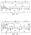
- the isolation structures shown in FIGURES 1A-1G are representative of STI structures.
- a gate dielectric film 45 is formed over the semiconductor substrate 10 which will form part of the NMOS and PMOS transistor structure. This gate dielectric can comprise silicon oxide, silicon oxynitride, silicon nitride or any suitable material.
- the FLASH memory cell shown in 90 comprises an n-type drain region 72 and an n-type source region 74.
- the FLASH memory cell also comprises a gate dielectric film 71, a floating gate 70, an interpoly dielectric layer 60 and a control gate 50.
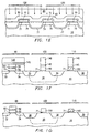
- the BARC etch is designed to have smaller etch biases.
- the Poly etch is designed to have less doped and undoped differences to increase margins for the n-type polycrystalline region 103 recess ( ⁇ 100 ⁇ ) due to SAS isolation etch process.
- FIGURE 1G Illustrated in FIGURE 1G is the structure of FIGURE 1F after removal of the resist film 140 and the BARC film 145.
- the embedded FLASH integrated circuit will be completed using standard semiconductor processing.
Landscapes
- Engineering & Computer Science (AREA)
- Manufacturing & Machinery (AREA)
- Semiconductor Memories (AREA)
- Non-Volatile Memory (AREA)
- Metal-Oxide And Bipolar Metal-Oxide Semiconductor Integrated Circuits (AREA)
Abstract
Description
- HBr
- 85-100 sccm
- O2
- 15-20 sccm
- Pressure
- 4-8 mTorr
- Source power
- 300-320 Watt
- Bias power
- 110-170 Watt
- Cathode Temp
- 55 °C
- Wall/Dome Temp
- 80/80 °C
- Etch Time
- Endpoint (3090Å wavelength) with 35% over-etch time
- CF4
- 30-60 sccm
- Pressure
- 3-7 mTorr
- Source power
- 400-800 Watt
- Bias power
- 25-60 Watt
- Cathode Temp
- 55 °C
- Wall/Dome Temp
- 80/80 °C
- Etch Time
- 10 s
- HBr
- 110-140 sccm
- Cl2
- 30-60 sccm
- HeO2
- 12-19 sccm
- Pressure
- 3-7 mTorr
- Source power
- 500-600 Watt
- Bias power
- 25-60 Watt
- Cathode Temp
- 55 °C
- Wall/Dome Temp
- 80/80 °C
- Etch Time
- 50 s
- HBr
- 130-170 sccm
- Cl2
- 60-80 sccm
- HeO2
- 15-20 sccm
- Pressure
- 8-15 mTorr
- Source power
- 300-450 Watt
- Bias power
- 50 Watt
- Cathode Temp
- 55 °C
- Wall/Dome Temp
- 80/80 °C
- Etch Time
- Endpoint (2880Å wavelength)
- HBr
- 130-170 sccm
- HeO2
- 9-13 sccm
- Pressure
- 90-120 mTorr
- Source power
- 700-900 Watt
- Bias power
- 100-250 Watt
- Cathode Temp
- 55 °C
- Wall/Dome Temp
- 80/80 °C
- Etch Time
- 65 s
Claims (12)
- A method of fabricating an integrated circuit which includes an embedded FLASH memory and an NMOS transistor, including doping a source line region for the FLASH memory and doping a gate electrode region for the NMOS transistor during the same doping step.
- A method as claimed in claim 1 including:forming a photo-resist film on a semiconductor substrate in which the integrated circuit is being fabricated,patterning the photo-resist film to expose a region which will serve as the source line region in the FLASH memory and an area of a polycrystalline silicon layer which will serve as the gate electrode region of the NMOS transistor andsimultaneously doping the exposed region and the exposed area of the polycrystalline silicon layer to provide the source line region of the FLASH memory and the gate electrode region of the NMOS transistor.
- A method as claimed in claim 1 or claim 2, including the step of removing a plurality of isolation regions separating the source regions of the FLASH memory prior to performing the doping step during which the source line region of the FLASH memory is formed.
- A method as claimed in claim 1, including:forming a photoresist film on a semiconductor substrate in which the integrated circuit is being fabricated,patterning the photoresist film to expose a region which will serve as a source line region for the FLASH memory and an area of a polycrystalline silicon layer which will serve as the gate electrode region of the NMOS transistor,removing a plurality of isolation regions which separate the source regions of the FLASH memory to expose the semiconductor substrate material under the isolation regions,simultaneously doping the exposed region and the exposed area of the polycrystalline silicon layer to provide the source line region of the FLASH memory and the gate electrode region of the NMOS transistor andpatterning and etching the polycrystalline silicon layer to form the gate electrode region for the NMOS transistor from the doped area of the polycrystalline silicon layer and a gate electrode region for a PMOS transistor from an undoped area of the polycrystalline silicon layer.
- A method as claimed in any one of claims 1 to 3, further including the step of patterning and etching the polycrystalline silicon layer to form the gate electrode for the NMOS transistor from the doped area of the polycrystalline silicon layer and a gate electrode region for a PMOS transistor from an undoped area of the polycrystalline silicon layer.
- A method as claimed in claim 5, including patterning and etching the polycrystalline silicon layer by steps including:forming an anti-reflective coating film on the polycrystalline silicon layer,forming a photoresist film on the anti-reflective coating film,patterning and removing portions of the photoresist film to expose both doped and undoped regions of the polycrystalline silicon film,etching the anti-reflective coating film to expose the unwanted part of the doped area of the polycrystalline silicon layer and the unwanted part of the undoped area of the polycrystalline silicon layer andsimultaneously etching the doped and undoped area of the polycrystalline silicon layer.
- A method as claimed in claim 6, wherein etching the anti-reflective coating film includes:effecting the flow of HBr in a plasma etcher at 85-100 sccm,effecting the flow of O2 in a plasma etcher at 15-20 sccm,maintaining a plasma etcher chamber pressure of 4-8 mTorr,maintaining a plasma etcher source power of 300-320 Watt,maintaining a plasma etcher bias power of 110-170 Watt,maintaining a plasma etcher cathode temperature of 55 °C;maintaining a plasma etcher Wall/Dome Temp of 80/80 °C anddetermining an etch time with a endpoint detector using a 3090Å wavelength with 35% over-etch time.
- A method as claimed in any one of claims 4 to 7 wherein the etching of the polycrystalline silicon layer includes:effecting the flow of HBr in a plasma etcher at 110-140 sccm,effecting the flow of Cl2 in a plasma etcher at 30-60 sccm,effecting the flow of HeO2 in a plasma etcher at 12-19 sccm,maintaining a plasma etcher chamber pressure of 3-7 mTorr,maintaining a plasma etcher source power of 500-600 Watt,maintaining a plasma etcher bias power of 25-60 Watt,maintaining a plasma etcher cathode temperature of 55 °C,maintaining a plasma etcher Wall and Dome Temp of 80°C anddetermining an etch time with a endpoint detector using a 2880Å wavelength.
- A method as claimed in any one of claims 1 to 8, wherein doping is effected by a dopant selected from the group consisting of phosphorous and arsenic.
- A method of patterning and simultaneously etching doped and undoped polycrystalline silicon including:providing a layer of polycrystalline silicon including doped and undoped regions,forming a anti-reflective coating film on the polycrystalline silicon layer,forming a photoresist film on the anti-reflective film,patterning and removing portions of the photoresist film to allow access to doped and undoped regions of the polycrystalline silicon layer,etching the anti-reflective coating film to expose unwanted doped and undoped parts of the polycrystalline silicon layer andsimultaneously etching the doped and undoped regions of said polycrystalline silicon film.
- A method as claimed in claim 10, wherein etching the anti-reflective coating film includes:effecting the flow of HBr in a plasma etcher at 85-100 sccm,effecting the flow of O2 in a plasma etcher at 15-20 sccm,maintaining a plasma etcher chamber pressure of 4-8 mTorr,maintaining a plasma etcher source power of 300-320 Watt,maintaining a plasma etcher bias power of 110-170 Watt,maintaining a plasma etcher cathode temperature of 55 °C;maintaining a plasma etcher Wall/Dome Temp of 80/80 °C anddetermining an etch time with a endpoint detector using a 3090Å wavelength with 35% over-etch time.
- A method as claimed in claim 10 or claim 11, wherein etching the doped and undoped regions of said polycrystalline silicon layer includes:effecting the flow of HBr in a plasma etcher at 110-140 sccm,effecting the flow of Cl2 in a plasma etcher at 30-60 sccm,effecting the flow of HeO2 in a plasma etcher at 12-19 sccm,maintaining a plasma etcher chamber pressure of 3-7 mTorr,maintaining a plasma etcher source power of 500-600 Watt,maintaining a plasma etcher bias power of 25-60 Watt,maintaining a plasma etcher cathode temperature of 55 °C;maintaining a plasma etcher Wall and Dome Temp of 80 °C; anddetermining an etch time with a endpoint detector using a 2880Å wavelength.
Applications Claiming Priority (2)
| Application Number | Priority Date | Filing Date | Title |
|---|---|---|---|
| US14379699P | 1999-07-14 | 1999-07-14 | |
| US143796P | 1999-07-14 |
Publications (2)
| Publication Number | Publication Date |
|---|---|
| EP1069614A2 true EP1069614A2 (en) | 2001-01-17 |
| EP1069614A3 EP1069614A3 (en) | 2007-12-12 |
Family
ID=22505684
Family Applications (1)
| Application Number | Title | Priority Date | Filing Date |
|---|---|---|---|
| EP00305834A Withdrawn EP1069614A3 (en) | 1999-07-14 | 2000-07-12 | Method of fabricating an integrated circuit |
Country Status (5)
| Country | Link |
|---|---|
| US (1) | US6451642B1 (en) |
| EP (1) | EP1069614A3 (en) |
| JP (1) | JP2001068571A (en) |
| KR (1) | KR20010029935A (en) |
| TW (1) | TW454345B (en) |
Cited By (1)
| Publication number | Priority date | Publication date | Assignee | Title |
|---|---|---|---|---|
| US6380031B1 (en) * | 1999-09-08 | 2002-04-30 | Texas Instruments Incorporated | Method to form an embedded flash memory circuit with reduced process steps |
Families Citing this family (3)
| Publication number | Priority date | Publication date | Assignee | Title |
|---|---|---|---|---|
| JP2004152878A (en) * | 2002-10-29 | 2004-05-27 | Toshiba Corp | Semiconductor storage device and method of manufacturing the same |
| US6828187B1 (en) * | 2004-01-06 | 2004-12-07 | International Business Machines Corporation | Method for uniform reactive ion etching of dual pre-doped polysilicon regions |
| KR20090026927A (en) * | 2007-09-11 | 2009-03-16 | 삼성전자주식회사 | Embedded semiconductor device and its manufacturing method |
Family Cites Families (17)
| Publication number | Priority date | Publication date | Assignee | Title |
|---|---|---|---|---|
| US4151021A (en) * | 1977-01-26 | 1979-04-24 | Texas Instruments Incorporated | Method of making a high density floating gate electrically programmable ROM |
| JPS56116670A (en) * | 1980-02-20 | 1981-09-12 | Hitachi Ltd | Semiconductor integrated circuit device and manufacture thereof |
| US4310380A (en) * | 1980-04-07 | 1982-01-12 | Bell Telephone Laboratories, Incorporated | Plasma etching of silicon |
| US4992134A (en) * | 1989-11-14 | 1991-02-12 | Advanced Micro Devices, Inc. | Dopant-independent polysilicon plasma etch |
| KR930007527B1 (en) * | 1990-09-22 | 1993-08-12 | 삼성전자 주식회사 | Nonvolatile semiconductor memory device having a storage cell array and circumference circuit and method for fabricating thereof |
| EP0573169A1 (en) * | 1992-06-02 | 1993-12-08 | National Semiconductor Corporation | Segment-erasable flash EPROM |
| US5441914A (en) * | 1994-05-02 | 1995-08-15 | Motorola Inc. | Method of forming conductive interconnect structure |
| US5665203A (en) * | 1995-04-28 | 1997-09-09 | International Business Machines Corporation | Silicon etching method |
| US5847427A (en) * | 1995-12-21 | 1998-12-08 | Kabushiki Kaisha Toshiba | Non-volatile semiconductor memory device utilizing an oxidation suppressing substance to prevent the formation of bird's breaks |
| US5702988A (en) * | 1996-05-02 | 1997-12-30 | Taiwan Semiconductor Manufacturing Company, Ltd. | Blending integrated circuit technology |
| US5908311A (en) * | 1996-07-25 | 1999-06-01 | National Semiconductor Corporation | Method for forming a mixed-signal CMOS circuit that includes non-volatile memory cells |
| US5759893A (en) * | 1996-12-05 | 1998-06-02 | Powerchip Semiconductor Corp. | Method of fabricating a rugged-crown shaped capacitor |
| JP3077630B2 (en) * | 1997-06-05 | 2000-08-14 | 日本電気株式会社 | Semiconductor device and manufacturing method thereof |
| KR100268923B1 (en) * | 1997-09-29 | 2000-10-16 | 김영환 | method for forming dual gate of semiconductor device |
| US6322714B1 (en) * | 1997-11-12 | 2001-11-27 | Applied Materials Inc. | Process for etching silicon-containing material on substrates |
| US6071779A (en) * | 1998-01-13 | 2000-06-06 | Texas Instruments Incorporated | Source line fabrication process for flash memory |
| US6265292B1 (en) * | 1999-07-12 | 2001-07-24 | Intel Corporation | Method of fabrication of a novel flash integrated circuit |
-
2000
- 2000-06-22 US US09/599,377 patent/US6451642B1/en not_active Expired - Lifetime
- 2000-07-12 EP EP00305834A patent/EP1069614A3/en not_active Withdrawn
- 2000-07-13 KR KR1020000040064A patent/KR20010029935A/en not_active Withdrawn
- 2000-07-14 JP JP2000214545A patent/JP2001068571A/en active Pending
- 2000-08-03 TW TW089114025A patent/TW454345B/en not_active IP Right Cessation
Cited By (1)
| Publication number | Priority date | Publication date | Assignee | Title |
|---|---|---|---|---|
| US6380031B1 (en) * | 1999-09-08 | 2002-04-30 | Texas Instruments Incorporated | Method to form an embedded flash memory circuit with reduced process steps |
Also Published As
| Publication number | Publication date |
|---|---|
| TW454345B (en) | 2001-09-11 |
| EP1069614A3 (en) | 2007-12-12 |
| JP2001068571A (en) | 2001-03-16 |
| US6451642B1 (en) | 2002-09-17 |
| KR20010029935A (en) | 2001-04-16 |
Similar Documents
| Publication | Publication Date | Title |
|---|---|---|
| JP3164026B2 (en) | Semiconductor device and manufacturing method thereof | |
| US6174758B1 (en) | Semiconductor chip having fieldless array with salicide gates and methods for making same | |
| US5894147A (en) | Memory transistor having underlapped floating gate | |
| US6346442B1 (en) | Methods for fabricating a semiconductor chip having CMOS devices and a fieldless array | |
| JP4027446B2 (en) | Nonvolatile memory manufacturing method | |
| US7276407B2 (en) | Method for fabricating semiconductor device | |
| US6465293B2 (en) | Method of manufacturing a flash memory cell | |
| US7919367B2 (en) | Method to increase charge retention of non-volatile memory manufactured in a single-gate logic process | |
| JP4633554B2 (en) | Method for manufacturing flash memory device | |
| US7384845B2 (en) | Methods of fabricating flash memory devices including word lines with parallel sidewalls | |
| US20040147099A1 (en) | Method of producing semiconductor device | |
| US6448137B1 (en) | Method of forming an NROM embedded with mixed-signal circuits | |
| US6773992B2 (en) | Method for fabricating nonvolatile-semiconductor memory device | |
| KR20010035857A (en) | semiconductor device and method for manufacturing the same | |
| US6110779A (en) | Method and structure of etching a memory cell polysilicon gate layer using resist mask and etched silicon oxynitride | |
| EP1222690B1 (en) | Method of manufacturing a semiconductor memory device with anti-reflective coating | |
| US6300184B1 (en) | Method of manufacturing a CMOS transistor | |
| US6451642B1 (en) | Method to implant NMOS polycrystalline silicon in embedded FLASH memory applications | |
| US6974999B2 (en) | Semiconductor device and method of manufacturing the same | |
| US6350638B2 (en) | Method of forming complementary type conductive regions on a substrate | |
| KR20050010260A (en) | Method of manufacturing NAND flash memory device | |
| JP3486331B2 (en) | Method for manufacturing semiconductor device | |
| US7125775B1 (en) | Method for forming hybrid device gates | |
| US20010026995A1 (en) | Method of forming shallow trench isolation | |
| US6391702B1 (en) | Method of manufacture for semiconductor devices |
Legal Events
| Date | Code | Title | Description |
|---|---|---|---|
| PUAI | Public reference made under article 153(3) epc to a published international application that has entered the european phase |
Free format text: ORIGINAL CODE: 0009012 |
|
| AK | Designated contracting states |
Kind code of ref document: A2 Designated state(s): AT BE CH CY DE DK ES FI FR GB GR IE IT LI LU MC NL PT SE |
|
| AX | Request for extension of the european patent |
Free format text: AL;LT;LV;MK;RO;SI |
|
| PUAL | Search report despatched |
Free format text: ORIGINAL CODE: 0009013 |
|
| AK | Designated contracting states |
Kind code of ref document: A3 Designated state(s): AT BE CH CY DE DK ES FI FR GB GR IE IT LI LU MC NL PT SE |
|
| AX | Request for extension of the european patent |
Extension state: AL LT LV MK RO SI |
|
| RIC1 | Information provided on ipc code assigned before grant |
Ipc: H01L 21/3213 20060101ALI20071108BHEP Ipc: H01L 27/105 20060101ALI20071108BHEP Ipc: H01L 21/8247 20060101AFI20001025BHEP |
|
| 17P | Request for examination filed |
Effective date: 20080612 |
|
| AKX | Designation fees paid |
Designated state(s): DE FR GB |
|
| 17Q | First examination report despatched |
Effective date: 20080909 |
|
| STAA | Information on the status of an ep patent application or granted ep patent |
Free format text: STATUS: THE APPLICATION IS DEEMED TO BE WITHDRAWN |
|
| 18D | Application deemed to be withdrawn |
Effective date: 20090320 |