EP1067778A2 - Electronic camera and its method of multiple exposure - Google Patents
Electronic camera and its method of multiple exposure Download PDFInfo
- Publication number
- EP1067778A2 EP1067778A2 EP00305498A EP00305498A EP1067778A2 EP 1067778 A2 EP1067778 A2 EP 1067778A2 EP 00305498 A EP00305498 A EP 00305498A EP 00305498 A EP00305498 A EP 00305498A EP 1067778 A2 EP1067778 A2 EP 1067778A2
- Authority
- EP
- European Patent Office
- Prior art keywords
- picture data
- picture
- frame
- memory
- npxl
- Prior art date
- Legal status (The legal status is an assumption and is not a legal conclusion. Google has not performed a legal analysis and makes no representation as to the accuracy of the status listed.)
- Withdrawn
Links
Images

Classifications
-
- H—ELECTRICITY
- H04—ELECTRIC COMMUNICATION TECHNIQUE
- H04N—PICTORIAL COMMUNICATION, e.g. TELEVISION
- H04N23/00—Cameras or camera modules comprising electronic image sensors; Control thereof
- H04N23/80—Camera processing pipelines; Components thereof
- H04N23/81—Camera processing pipelines; Components thereof for suppressing or minimising disturbance in the image signal generation
-
- H—ELECTRICITY
- H04—ELECTRIC COMMUNICATION TECHNIQUE
- H04N—PICTORIAL COMMUNICATION, e.g. TELEVISION
- H04N23/00—Cameras or camera modules comprising electronic image sensors; Control thereof
- H04N23/70—Circuitry for compensating brightness variation in the scene
-
- H—ELECTRICITY
- H04—ELECTRIC COMMUNICATION TECHNIQUE
- H04N—PICTORIAL COMMUNICATION, e.g. TELEVISION
- H04N23/00—Cameras or camera modules comprising electronic image sensors; Control thereof
- H04N23/70—Circuitry for compensating brightness variation in the scene
- H04N23/76—Circuitry for compensating brightness variation in the scene by influencing the image signals
Definitions
- the present invention relates to an electronic camera, which outputs an optical image of a subject converted into an electronic signal, particularly, relates to an electronic camera having a function of multiple exposures and its method of multiple exposure.
- Such cameras as an electronic still camera of taking a still-picture and a video camera of taking a motion picture are constituted of that a picture signal obtained by an image sensing device is inputted into an automatic gain control (AGC) circuit and the picture signal is inputted into an analog to digital (A/D) converter after a level of the picture signal has been adjusted to an optimum level.
- AGC automatic gain control
- A/D analog to digital
- a method of decreasing an output level of an image sensing device by stopping down light intensity in an optical system or by shortening one exposure time is conceivable.
- S/N signal to noise ratio
- Another method of that an already accumulated data and a newly accumulating data are divided into two and then they are added while accumulating a picture data is also conceivable.
- information about a picture data accumulated first becomes 1/2 m-1 , wherein "m" is a number of multiple exposures and is an integer of being greater than or equal to 2.
- an object of the present invention is to provide an electronic camera, which can obtain a multi-exposed picture in proper exposure without deteriorating a signal to noise ratio (S/N) of output of an image sensing device or overflowing a memory capacity, with balancing picture information obtained at each exposure during a multiple exposure process.
- S/N signal to noise ratio
- the present invention provides, according to an aspect thereof, an electronic camera, which can perform multiple exposures, comprising image sensing means for outputting an optical image of a subject after converting the optical image into an electric signal; analog to digital converting means for converting a picture signal obtained by the image sensing means into a digital picture data; and memory means for storing the digital picture data corresponding to a picture of one frame
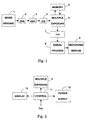
- Fig. 1 is a block diagram of an electronic camera according to an embodiment of the present invention.
- an electronic camera comprises an image sensing device 1, a correlation double sampling (CDS) circuit 2, an automatic gain control (AGC) circuit 3, an analog to digital (A/D) converter circuit 4, a multiple exposure control circuit 5, a frame memory 6, a divider circuit 7, a signal processing circuit 8 and a recording medium 9.
- CDS correlation double sampling
- AGC automatic gain control
- A/D analog to digital
- the image sensing device 1 converts an optical image of a subject, which is obtained by an optical system not shown, into an electric signal.
- the CDS circuit 2 eliminates a readout clock from an output signal of the image sensing device 1.
- the AGC circuit 3 maintains a signal level at constant level.
- the A/D converter circuit 4 converts an output signal from the AGC circuit 3 into a digital signal, wherein a digital signal is hereinafter called a picture data.
- the frame memory 6 stores a picture data of one picture frame.
- the multiple exposure control circuit 5 controls to add a picture data stored in the frame memory 6 and a new picture data to be inputted and to store them in the frame memory 6 when performing a multiple exposure process.
- the divider circuit 7 divides a value in response to each pixel of a signal read out from the frame memory 6 through the multiple exposure control circuit 5 by a number of exposures "m".
- the signal processing circuit 8 generates a luminance signal and a color-difference signal from an output signal of the divider 7 and records them in the recording medium 9 through an information compression process.
- the frame memory 6 has a memory capacity of "M” bits, which is expressed by an equation (1) below in response to a number of exposures "m", wherein the "m” is an integer of being greater than or equal to 2.
- N (N + k ⁇ nPXL) (1) , where "N” is a necessary capacity for a single exposure in bit, "k” is an integer of satisfying an inequality 2 k-1 ⁇ m ⁇ 2 k and nPXL is a number of pixels in one picture frame.
- a data of integrating "m” times a data of "n” bits multiplied by a data of "n” bits becomes a data of (n + k) bits, wherein the "k” satisfies the inequality 2 k-1 ⁇ m ⁇ 2 k .
- the capacity "N” is equivalent to "n ⁇ nPXL”.
- the frame memory 6 can store a picture data of integrated "m” times without overflowing by setting the memory capacity of the frame memory 6 to a capacity "M", which is a sum of the capacity "N” and (k ⁇ nPXL).
- the multiple exposure control circuit 5 performs a process of integrating a picture data outputted from the A/D converter circuit 4 by a number of multiple exposures "m" at each pixel. In other words, at a first exposure, that is, when a picture data is taken in, the multiple exposure control circuit 5 makes the frame memory 6 store the picture data as it is. At a second and succeeding exposures, the multiple exposure control circuit 5 processes to add a picture data read out from the frame memory 6 to another picture data outputted from the A/D converter circuit 4 pixel by pixel and to store the added picture data in the frame memory 6 once again.
- a picture data is read out from the frame memory 6 through the multiple exposure control circuit 5.
- a picture data value of each pixel is divided by "m” by the divider circuit 7 and the divided picture data is supplied to the signal processing circuit 8.
- a picture data supplied to the signal processing circuit 8 is averaged by equally weighting picture data obtained by "m" times exposures, that is, obtained by taking in data "m” times. Accordingly, an information of a picture taken in first will not be decreased extremely. Further, a process such as stopping down light intensity is not performed, so that a multi-exposed still picture data having an excellent signal to noise ratio (S/N) can be obtained.
- S/N signal to noise ratio
- the picture data inputted to the signal processing circuit 8 is converted into a luminance signal and a color-difference signal and recorded in the recording medium 9 after an information compression process is applied.
- a semiconductor memory and a magnetic memory are utilized for the recording medium 9.
- Fig. 2 shows a block diagram of an electronic camera depicting a control function during multiple exposure according to the embodiment of the present invention.
- Fig. 3 shows a flow chart of processing steps during multiple exposure according to the embodiment of the present invention.
- a control section 11 is composed of a micro computer and controls the multiple exposure control circuit 5, a power supply section 12 and a display section 13 in accordance with processing steps shown in Fig. 3.
- An interval "Tint" of multiple exposure that is, an interval "Tint” between each exposure is inputted by a user through an operation section not shown in the control section 11.
- a picture data is taken in first, that is, a first time exposure is performed (step S11) when a multiple exposure is started.
- a counting number "i” of a counter which counts a number of exposures, is set to “1” (step S12).
- the interval “Tint” is judged whether or not the “Tint” is longer than a predetermined interval “Tint0" (step S13). In a case of "Tint ⁇ Tint0", the process is forwarded to a step S18.
- step S13 In a case of "Tint > Tint 0" in the step S13, while power is continuously supplied to minimum necessary circuits, power supply to other circuits is shut off so as to save power consumption (step S14) and the display section 13 indicates that it is in a standby mode for multiple exposure (step S15).
- the standby mode continues until an indication of count-up timer "tmINT", which counts a lapse of time after a preceding picture data is taken in, exceeds a time of subtracting a time allowance "DT" from the interval "Tint” (step S16), wherein the time allowance "DT" is defined as a time duration from a time when power is resupplied to a time when a circuit status becomes stable. Accordingly, with resupplying power prior to taking in a succeeding picture data mentioned above, functions such as automatic white balancing and automatic focusing can be prevented from shifting when the picture data is taken in.
- step S16 if the lapse of time is " tmINT > Tint - DT ", power is resupplied to the other circuits of which power is shut off in the step S14 (step S17).
- the other circuits keep in a standby mode and the process repeats until the interval "Tint" lapses after a preceding picture data is taken in (step S18).
- a succeeding picture data is taken in, that is, a succeeding picture is exposed when the interval "Tint” lapses (step S19) and the counting number "i” of the counter is advanced with an increment of 1 (step S20).
- the process returns back to the step S13 until the counting number "i" of the counter becomes the number of exposures "m”.
- the process comes to end when the counting number "i” of the counter becomes “m” (step S21). If the lapse of time is "tmINT ⁇ Tint - DT" in the step S16, the process returns back to the step S15.
- values in response to each pixel of the picture data obtained by the integration are outputted after being decreased by a factor of 1/m, so that a multi-exposed picture in optimum exposure can be obtained with balancing a picture information obtained at each exposure of multiple exposures without decreasing S/N of output of an image sensing device or without overflowing of a memory capacity.
Landscapes
- Engineering & Computer Science (AREA)
- Multimedia (AREA)
- Signal Processing (AREA)
- Transforming Light Signals Into Electric Signals (AREA)
- Television Signal Processing For Recording (AREA)
- Studio Devices (AREA)
Abstract
Description
Claims (2)
- An electronic camera, which can perform multiple exposures, comprising:image sensing means for outputting an optical image of a subject after converting the optical image into an electric signal;analog to digital converting means for converting a picture signal obtained by said image sensing means into a digital picture data; andmemory means for storing the digital picture data corresponding to a picture of one frame,said electronic camera is further characterized by that said memory means has a memory capacity of "M" bits defined by an equation mentioned below in response to a number of multiple exposures "m", wherein the "m" is an integer of being greater than or equal to 2, and that the digital picture data is integrated by the number of multiple exposures "m" and stored in said memory means, and that a value corresponding to each pixel of the picture data obtained by the integration is decreased by a factor of 1/m and outputted:
- A method of multiple exposure of an electronic camera comprising steps of:outputting an optical image of a subject after converting the optical image into an electric signal;converting a picture signal in analog obtained in the step of outputting into a digital picture data; andstoring the digital picture data corresponding to a picture of one frame in memory means,
wherein said memory means has a memory capacity of "M" bits defined by an equation mentioned below in response to a number of multiple exposures "m", wherein the "m" is an integer of being greater than or equal to 2, and wherein the digital picture data is integrated by the number of multiple exposures "m" and stored in said memory means, and wherein a value corresponding to each pixel of the picture data obtained by the integration is decreased by a factor of 1/m and outputted:
Applications Claiming Priority (2)
| Application Number | Priority Date | Filing Date | Title |
|---|---|---|---|
| JP19168199 | 1999-07-06 | ||
| JP11191681A JP2001024941A (en) | 1999-07-06 | 1999-07-06 | Electronic camera |
Publications (2)
| Publication Number | Publication Date |
|---|---|
| EP1067778A2 true EP1067778A2 (en) | 2001-01-10 |
| EP1067778A3 EP1067778A3 (en) | 2002-09-11 |
Family
ID=16278694
Family Applications (1)
| Application Number | Title | Priority Date | Filing Date |
|---|---|---|---|
| EP00305498A Withdrawn EP1067778A3 (en) | 1999-07-06 | 2000-06-29 | Electronic camera and its method of multiple exposure |
Country Status (2)
| Country | Link |
|---|---|
| EP (1) | EP1067778A3 (en) |
| JP (1) | JP2001024941A (en) |
Cited By (5)
| Publication number | Priority date | Publication date | Assignee | Title |
|---|---|---|---|---|
| EP1347635A3 (en) * | 2002-03-18 | 2005-01-26 | Creo IL. Ltd. | Method and apparatus for capturing images using blemished sensors |
| EP1509040A3 (en) * | 2003-08-20 | 2006-07-12 | Lg Electronics Inc. | Method for managing digital slow shutter mode in monitor camera |
| WO2010072718A1 (en) * | 2008-12-22 | 2010-07-01 | Thomson Licensing | Method and device to capture images by emulating a mechanical shutter |
| US8077208B2 (en) | 2004-11-18 | 2011-12-13 | Nokia Corporation | Method, apparatus, software and arrangement for modifying image data |
| US11039099B2 (en) | 2016-11-24 | 2021-06-15 | Sony Semiconductor Solutions Corporation | Solid-state imaging element, solid-state imaging apparatus, and method for controlling solid-state imaging element |
Families Citing this family (2)
| Publication number | Priority date | Publication date | Assignee | Title |
|---|---|---|---|---|
| US7600138B2 (en) * | 2004-11-09 | 2009-10-06 | Timken Us Corporation | Low power ASIC circuit |
| JP6218480B2 (en) * | 2013-07-30 | 2017-10-25 | キヤノン株式会社 | Electronic device and control method thereof |
Family Cites Families (2)
| Publication number | Priority date | Publication date | Assignee | Title |
|---|---|---|---|---|
| JP2921879B2 (en) * | 1989-09-29 | 1999-07-19 | 株式会社東芝 | Image data processing device |
| JPH0918793A (en) * | 1995-06-26 | 1997-01-17 | Nikon Corp | Imaging device |
-
1999
- 1999-07-06 JP JP11191681A patent/JP2001024941A/en active Pending
-
2000
- 2000-06-29 EP EP00305498A patent/EP1067778A3/en not_active Withdrawn
Cited By (8)
| Publication number | Priority date | Publication date | Assignee | Title |
|---|---|---|---|---|
| EP1347635A3 (en) * | 2002-03-18 | 2005-01-26 | Creo IL. Ltd. | Method and apparatus for capturing images using blemished sensors |
| US7120315B2 (en) | 2002-03-18 | 2006-10-10 | Creo Il., Ltd | Method and apparatus for capturing images using blemished sensors |
| EP1509040A3 (en) * | 2003-08-20 | 2006-07-12 | Lg Electronics Inc. | Method for managing digital slow shutter mode in monitor camera |
| US7580067B2 (en) | 2003-08-20 | 2009-08-25 | Lg Electronics Inc. | Method for managing digital slow shutter mode in monitor camera |
| US8077208B2 (en) | 2004-11-18 | 2011-12-13 | Nokia Corporation | Method, apparatus, software and arrangement for modifying image data |
| WO2010072718A1 (en) * | 2008-12-22 | 2010-07-01 | Thomson Licensing | Method and device to capture images by emulating a mechanical shutter |
| US9237276B2 (en) | 2008-12-22 | 2016-01-12 | Thomson Licensing | Method and device to capture images by emulating a mechanical shutter |
| US11039099B2 (en) | 2016-11-24 | 2021-06-15 | Sony Semiconductor Solutions Corporation | Solid-state imaging element, solid-state imaging apparatus, and method for controlling solid-state imaging element |
Also Published As
| Publication number | Publication date |
|---|---|
| JP2001024941A (en) | 2001-01-26 |
| EP1067778A3 (en) | 2002-09-11 |
Similar Documents
| Publication | Publication Date | Title |
|---|---|---|
| US5767904A (en) | Electronic still camera and method of controlling shutter | |
| Kuno et al. | A new automatic exposure system for digital still cameras | |
| US7362370B2 (en) | Image capturing apparatus, image capturing method, and computer-readable medium storing program using a distance measure for image correction | |
| US7995912B2 (en) | Imaging apparatus with strobe consecutive shooting mode and optional pixel addition drive | |
| USRE44278E1 (en) | Imaging system where a quick return mirror is returned to a down state and a stop is returned to a fully open state before the accumulation period ends | |
| US20030202115A1 (en) | Image capturing device performing divided exposure | |
| US7046275B1 (en) | Digital camera and imaging method | |
| US7161629B2 (en) | Electronic camera and method for calculating an exposure amount | |
| US6710808B1 (en) | Image sensing apparatus | |
| US7254276B2 (en) | Noise reduction in image capturing apparatus | |
| US6965410B1 (en) | Image sensing apparatus employing dark image data to correct dark noise | |
| US7301572B2 (en) | Pixel correction processing apparatus, image processing apparatus, pixel correction processing method, program, and storage medium | |
| US20030095299A1 (en) | Image sensing apparatus | |
| US7292268B2 (en) | Image processing system, image capturing apparatus, image processing apparatus, and image processing method for performing edge enhancement | |
| US7260267B2 (en) | Image processing apparatus, computer readable medium storing program, image processing method, image capturing apparatus, printing apparatus, and scanning apparatus | |
| US7475266B2 (en) | Image capturing apparatus that performs dynamic frequency control of buffer memory during moving image capture | |
| US20040066464A1 (en) | Image sensing apparatus, image sensing method, program, and recording medium | |
| JPH0336886A (en) | Still video camera | |
| JP2001024941A (en) | Electronic camera | |
| US20110279696A1 (en) | Imaging apparatus and information display method for imaging apparatus | |
| JPH0556343A (en) | Electronic image pickup device | |
| JPH05236422A (en) | Image recorder | |
| JP3155830B2 (en) | Imaging device | |
| JP3064948B2 (en) | An electronic camera that can change the compression ratio of image information | |
| JP3244727B2 (en) | Imaging device and imaging method |
Legal Events
| Date | Code | Title | Description |
|---|---|---|---|
| PUAI | Public reference made under article 153(3) epc to a published international application that has entered the european phase |
Free format text: ORIGINAL CODE: 0009012 |
|
| AK | Designated contracting states |
Kind code of ref document: A2 Designated state(s): AT BE CH CY DE DK ES FI FR GB GR IE IT LI LU MC NL PT SE |
|
| AX | Request for extension of the european patent |
Free format text: AL;LT;LV;MK;RO;SI |
|
| PUAL | Search report despatched |
Free format text: ORIGINAL CODE: 0009013 |
|
| AK | Designated contracting states |
Kind code of ref document: A3 Designated state(s): AT BE CH CY DE DK ES FI FR GB GR IE IT LI LU MC NL PT SE |
|
| AX | Request for extension of the european patent |
Free format text: AL;LT;LV;MK;RO;SI |
|
| AKX | Designation fees paid | ||
| REG | Reference to a national code |
Ref country code: DE Ref legal event code: 8566 |
|
| STAA | Information on the status of an ep patent application or granted ep patent |
Free format text: STATUS: THE APPLICATION IS DEEMED TO BE WITHDRAWN |
|
| 18D | Application deemed to be withdrawn |
Effective date: 20030312 |