EP1067663A2 - Switching power source - Google Patents
Switching power source Download PDFInfo
- Publication number
- EP1067663A2 EP1067663A2 EP00112085A EP00112085A EP1067663A2 EP 1067663 A2 EP1067663 A2 EP 1067663A2 EP 00112085 A EP00112085 A EP 00112085A EP 00112085 A EP00112085 A EP 00112085A EP 1067663 A2 EP1067663 A2 EP 1067663A2
- Authority
- EP
- European Patent Office
- Prior art keywords
- switching
- voltage
- power source
- load
- oscillation
- Prior art date
- Legal status (The legal status is an assumption and is not a legal conclusion. Google has not performed a legal analysis and makes no representation as to the accuracy of the status listed.)
- Withdrawn
Links
Images


Classifications
-
- H—ELECTRICITY
- H02—GENERATION; CONVERSION OR DISTRIBUTION OF ELECTRIC POWER
- H02M—APPARATUS FOR CONVERSION BETWEEN AC AND AC, BETWEEN AC AND DC, OR BETWEEN DC AND DC, AND FOR USE WITH MAINS OR SIMILAR POWER SUPPLY SYSTEMS; CONVERSION OF DC OR AC INPUT POWER INTO SURGE OUTPUT POWER; CONTROL OR REGULATION THEREOF
- H02M7/00—Conversion of AC power input into DC power output; Conversion of DC power input into AC power output
- H02M7/02—Conversion of AC power input into DC power output without possibility of reversal
- H02M7/04—Conversion of AC power input into DC power output without possibility of reversal by static converters
- H02M7/06—Conversion of AC power input into DC power output without possibility of reversal by static converters using discharge tubes without control electrode or semiconductor devices without control electrode
-
- H—ELECTRICITY
- H02—GENERATION; CONVERSION OR DISTRIBUTION OF ELECTRIC POWER
- H02M—APPARATUS FOR CONVERSION BETWEEN AC AND AC, BETWEEN AC AND DC, OR BETWEEN DC AND DC, AND FOR USE WITH MAINS OR SIMILAR POWER SUPPLY SYSTEMS; CONVERSION OF DC OR AC INPUT POWER INTO SURGE OUTPUT POWER; CONTROL OR REGULATION THEREOF
- H02M3/00—Conversion of DC power input into DC power output
- H02M3/22—Conversion of DC power input into DC power output with intermediate conversion into AC
- H02M3/24—Conversion of DC power input into DC power output with intermediate conversion into AC by static converters
- H02M3/28—Conversion of DC power input into DC power output with intermediate conversion into AC by static converters using discharge tubes with control electrode or semiconductor devices with control electrode to produce the intermediate AC
- H02M3/325—Conversion of DC power input into DC power output with intermediate conversion into AC by static converters using discharge tubes with control electrode or semiconductor devices with control electrode to produce the intermediate AC using devices of a triode or a transistor type requiring continuous application of a control signal
- H02M3/335—Conversion of DC power input into DC power output with intermediate conversion into AC by static converters using discharge tubes with control electrode or semiconductor devices with control electrode to produce the intermediate AC using devices of a triode or a transistor type requiring continuous application of a control signal using semiconductor devices only
- H02M3/33507—Conversion of DC power input into DC power output with intermediate conversion into AC by static converters using discharge tubes with control electrode or semiconductor devices with control electrode to produce the intermediate AC using devices of a triode or a transistor type requiring continuous application of a control signal using semiconductor devices only with automatic control of the output voltage or current, e.g. flyback converters
- H02M3/33523—Conversion of DC power input into DC power output with intermediate conversion into AC by static converters using discharge tubes with control electrode or semiconductor devices with control electrode to produce the intermediate AC using devices of a triode or a transistor type requiring continuous application of a control signal using semiconductor devices only with automatic control of the output voltage or current, e.g. flyback converters with galvanic isolation between input and output of both the power stage and the feedback loop
-
- H—ELECTRICITY
- H02—GENERATION; CONVERSION OR DISTRIBUTION OF ELECTRIC POWER
- H02M—APPARATUS FOR CONVERSION BETWEEN AC AND AC, BETWEEN AC AND DC, OR BETWEEN DC AND DC, AND FOR USE WITH MAINS OR SIMILAR POWER SUPPLY SYSTEMS; CONVERSION OF DC OR AC INPUT POWER INTO SURGE OUTPUT POWER; CONTROL OR REGULATION THEREOF
- H02M1/00—Details of apparatus for conversion
- H02M1/0003—Details of control, feedback or regulation circuits
- H02M1/0032—Control circuits allowing low power mode operation, e.g. in standby mode
-
- Y—GENERAL TAGGING OF NEW TECHNOLOGICAL DEVELOPMENTS; GENERAL TAGGING OF CROSS-SECTIONAL TECHNOLOGIES SPANNING OVER SEVERAL SECTIONS OF THE IPC; TECHNICAL SUBJECTS COVERED BY FORMER USPC CROSS-REFERENCE ART COLLECTIONS [XRACs] AND DIGESTS
- Y02—TECHNOLOGIES OR APPLICATIONS FOR MITIGATION OR ADAPTATION AGAINST CLIMATE CHANGE
- Y02B—CLIMATE CHANGE MITIGATION TECHNOLOGIES RELATED TO BUILDINGS, e.g. HOUSING, HOUSE APPLIANCES OR RELATED END-USER APPLICATIONS
- Y02B70/00—Technologies for an efficient end-user side electric power management and consumption
- Y02B70/10—Technologies improving the efficiency by using switched-mode power supplies [SMPS], i.e. efficient power electronics conversion e.g. power factor correction or reduction of losses in power supplies or efficient standby modes
Definitions
- the present invention relates to a switching power source and, particularly, to a switching power source capable of reducing a standby power consumption of an electronic device as a load.
- a conventional switching power source has been designed such that the power source efficiency becomes maximum for a load operating in a steady state. That is, the switching power source has been designed such that the power source efficiency becomes maximum for only a load of the switching power source, which is operating normally and there has been no measure taken for power consumption when the load of the switching power source is light or the load is in a standby state.
- a switching frequency thereof during the standby state of the load is lowered. In such case, however, audible sound may be generated by the transformer.
- the intermittent oscillation control is performed regardless of the voltage waveform of the commercial power source. Therefore, when the control is performed such that an oscillator oscillates during a time period other than a time period in which a charging capacitor constituting a primary side of a smoothing circuit for rectifying and smoothing a commercial power source voltage is charged, voltage ripple of the capacitor is increased, so that an output voltage on a secondary side of the smoothing circuit is varied.
- the oscillation is stopped every half-wave rectified output of a commercial input power source although the intermittent oscillation control is performed correspondingly to the voltage waveform of the commercial power source. That is, the control is performed such that the oscillation is persistent for a half cycle of the commercial power source and is stopped for the other half cycle thereof. Therefore, the oscillation is persistent even for the period other than the period in which the charging of a primary side capacitor is performed and the above mentioned problem of the secondary side voltage variation is not solved.
- An object of the present invention is to provide a switching power source including a switching transformer and capable of restricting voltage variation on a secondary side of the switching transformer when an intermittent oscillation for obtaining a switching operation of the switching power source is performed under a light load condition thereof.
- a switching power source device which includes a rectifier, a switching transformer and a switching element and in which an input A.C. voltage is rectified by the rectifier and smoothed by a smoothing capacitor and a resultant D.C. voltage is supplied to a primary side of the switching transformer while on/off controlling the D.C. voltage by the switching element and an A.C. voltage obtained in a secondary side of the switching transformer is rectified and smoothed and a resultant D.C. voltage is supplied to a load of the switching power source device, is featured by comprising comparator means for comparing a D.C. voltage obtained by rectifying the input A.C. voltage with a reference voltage and control means for detecting a state of the load of the switching power source and intermittently controlling a switching operation of the switching element according to an output of the comparator means when the load is light.
- the comparator means includes a comparator circuit for comparing the rectified D.C. voltage with the reference voltage and generating the output of the comparator means when the rectified D.C. voltage is larger than the reference voltage and the control means performs the intermittent control correspondingly to the output of the comparator means when the load is light. Further, the control means detects the state of the light load on the basis of a current supplied to the load. Alternatively, the control means detects the state of the light load by an external signal.
- the oscillation In intermittently controlling an oscillation for switching a power source device during a light load condition in order to reduce power consumption in a standby state thereof, the oscillation is allowed in only a peak time of an input A.C. power and a vicinity thereof and inhibited in other time period. Therefore, it becomes possible to oscillate in only a charging time of the smoothing capacitor on the primary side of the switching transformer to thereby minimize a voltage variation on the secondary side of the switching transformer.
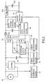
- Fig. 1 is a circuit diagram showing a switching power source according to an embodiment of the present invention.
- a voltage of a commercial power source 10 is rectified by a rectifier circuit 11, smoothed by a smoothing capacitor C1 and supplied to a primary side of a switching transformer T1.
- the switching power source includes a switching transistor Q1 as a switching element.
- the switching transistor Q1 as well as the rectified and smoothed D.C. voltage supplied to the primary side of the switching transformer T1 is ON/OFF controlled under an oscillation control of a switching control circuit 13.
- An output of a secondary side of the switching transformer T1 is rectified by a diode D1, smoothed by a capacitor C2 and supplied to a load, which is not shown, through a regulator IC1 as a D.C. voltage.
- a diode D1 An output of a secondary side of the switching transformer T1 is rectified by a diode D1, smoothed by a capacitor C2 and supplied to a load, which is not shown, through a regulator IC1 as a D.C. voltage.
- a regulator IC1 as a D.C. voltage.
- an element depicted by C3 is a capacitor.
- An error voltage detector circuit 22 is provided for detect a voltage supplied to the load.
- the error voltage detector circuit 22 compares the rectified and smoothed output voltage of the switching transformer T1 with a reference voltage to detect a difference therebetween, which is supplied to the switching control circuit 13 through an error voltage transmission circuit 16.
- the duty cycle of an oscillation signal of the switching transistor Q1 is controlled by the switching control circuit 13 according to the voltage difference signal from the error transmission circuit 16 to maintain the output voltage of the switching power source constant.
- the switching power source further includes a current detection circuit 21 for detecting a current supplied to the load.
- the current detector circuit 21 activates a signal transmission circuit 15 such that a signal for controlling the intermittent oscillation from the intermittent oscillation control circuit 12 provided on the primary side of the switching transformer 11 is transmitted to a signal transmission circuit 14.
- the intermittent oscillation control circuit 12 has a function of comparing the rectified voltage of the commercial power source 10 with a reference voltage and the switching control circuit 13 is controlled by an output of the intermittent oscillation control circuit 12 through the signal transmission circuits 15 and 14 to repeatedly switch the switching transistor Q1 between oscillation and non-oscillation states. Switching loss of the switching transistor Q1 in intermittent oscillation state when the load is light is reduced, so that the power source efficiency can be improved.
- the current detector circuit 21 has the function of detecting the output current of the switching power source and comparing the output current with the setting current.
- the signal transmission circuit 15 is activated by the output current detected by the current detector circuit 21 to transmit the comparison signal from the intermittent oscillation control circuit 12 to the switching control signal 13 through the signal transmission circuit 14. Therefore, the signal transmission circuit 15 has a role of a comparison output switch of the intermittent oscillation control circuit 12.
- the signal transmission circuit 15 is activated to pass the output of the intermittent oscillation control circuit 12 to the signal transmission circuit 14.
- the signal transmission circuit 15 is deactivated to block the output of the intermittent oscillation control circuit 12 to the signal transmission circuit 14.
- the intermittent oscillation control circuit 12 has a function of generating a D.C. voltage from the A.C. voltage of the commercial power source 10 and compares the D.C. voltage with a reference voltage. As a result of comparison outputted from the intermittent oscillation control circuit 12 is transmitted to the switching control circuit 13 through the signal transmission circuit 14. When the output current of the switching power source becomes smaller than the setting current, the switching control circuit 13 responds to the signal from the intermittent oscillation control circuit 12 to repeatedly switch the switching operation of the switching transistor Q1 between oscillation state and non-oscillation state.
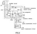
- Fig. 2 is a detailed circuit diagram of the intermittent oscillation control circuit 12 shown in Fig. 1.
- the intermittent oscillation control circuit 12 is constructed, basically, with a rectifier circuit 51 for rectifying the A.C. voltage of the commercial power source 10 to obtain the D.C. voltage and a comparator 52.
- the comparator 52 compares a half-wave rectified voltage from a diode D43 with a reference voltage 53.
- An output of the comparator 52 can be variable by changing a setting value of the reference voltage 53.
- the rectifier circuit 51 is constructed with capacitors C41 and C42, diodes D41 and D42 and a Zener diode ZD41.
- the rectifier circuit 51 itself is not constitute the present invention. Its construction is not limited to that shown in Fig. 2 and any other construction may be used on demand.
- Fig. 1 when the output current of the switching power source exceeds the setting current of the current detector circuit 21, the signal transmission circuit 15 becomes in an OFF state. Therefore, the output signal of the intermittent oscillation control circuit 12 is not transmitted to the signal transmission circuit 14, so that the switching control circuit 13 performs a normal oscillation control operation.
- the output current of the switching power source is reduced when the load is varied by change of the state of the load from a normal operation state to a standby state, the output current may become smaller than the setting current.
- the current detector circuit 21 causes the signal transmission circuit 15 to turn ON.
- the output signal of the intermittent oscillation control circuit 12 can be transmitted to the signal transmission circuit 14 and controls the switching control circuit 13.
- the switching control circuit 13 ON and OFF in this manner, the switching transistor Q1 as the main switch element can be switched between the oscillation state and the non-oscillation state.
- the rectifier circuit 51 half-wave rectifies the A.C. voltage of the commercial power source 10 by means of the diode D43 thereof to obtain a half-wave rectified D.C. voltage and the half-wave rectified D.C. voltage is supplied to one input of the comparator 52.
- the half-wave rectified D.C. voltage can be arbitrarily set by changing a threshold value of the Zener diode ZD41, provided that the half-wave rectified D.C. voltage is within a power source voltage range of the comparator 52.
- a loss in the comparator 52 may be increased if the power source voltage of the comparator 52 is set to a certain high value, it is preferable in this embodiment to set the half-wave rectified D.C. voltage to 5V.
- the reference voltage 53 and the half-wave rectified D.C. voltage, which has a waveform shown by B in Fig. 3 and divided by the resistors R41 and R42 are inputted to the comparator 52.
- the half-wave rectified D.C. voltage is compared with the reference voltage 53 in the comparator 52 and a signal having a waveform shown by C in Fig. 3 is outputted from the comparator 52. Width of the ON portion of the output waveform C of the comparator 52 can be changed by changing the setting value of the reference voltage 53.
- the ON width of the output waveform of the comparator 52 By setting the ON width of the output waveform of the comparator 52 to a period corresponding to the charging period of the smoothing capacitor C1 on the primary side of the switching transformer T1, it is possible to oscillate the switching transistor Q1 for only the charging period of the capacitor C1 and to stop the oscillation thereof for other time period to thereby eliminate ripple on the secondary side of the switching transformer T1.
- the ON width of the switching waveform of the switching transistor Q1 in Fig. 3 can be freely changed by changing the setting value of the reference voltage 53, it is possible when the output ripple is increased by the intermittent oscillation, to prevent any trouble due to ripple from occurring by reducing the ON width.
- the output waveform C of the comparator 52 controls the switching control circuit 13 through the signal transmission circuit 14.
- an intermittent oscillation waveform D of the transistor Q1 shown in Fig. 3 is obtained. That is, by providing the OFF period of the oscillation of the switching transistor Q1, it becomes possible to reduce the switching loss on the primary side of the switching transformer T1.
- This intermittent operation of the switching power source attributes to reduction of the power consumption of the switching power source.
- the signal from the current detector circuit 21 turns the signal transmission circuit 15 OFF, so that the output of the intermittent oscillation control circuit 12 is not transmitted to the switching control circuit 13.
- the intermittent oscillation of the switching transistor Q1 is changed to a continuous oscillation and the usual operation of the switching power source is automatically recovered.
- the signal transmission circuits 14 and 15 are constructed by using known photo-couplers, respectively, as shown in Fig. 2, the constructions of the signal transmission circuits are not limited thereto.
- the normal operation state of the load and the standby state of the load are determined by utilizing the output of the current detector circuit 21.
- the load device includes a micro processor 23 as shown in Fig. 4, it is possible that the micro processor 23 determines the state of the load and sends the state information of the load directly to the signal transmission circuit 15 to ON/OFF control the output of the intermittent oscillation control circuit 12.
- a micro processor detects a remote control operation for turning a power source on.
- the signal transmission circuit 15 may be activated by a detection signal from the micro processor.
- the switching power source can be constructed with using a single power source, without requiring any power source dedicated to the light load or dedicated to the standby state of the load. That is, since the switching loss when the load is light is reduced, the present invention can be applied to a switching power source having any capacity. Further, the switching transformer of the switching power source does not produce audible sound.
- the intermittent oscillation operation is performed by a repeated ON/OFF operation of the switching transistor without changing the switching frequency thereof. Further, the voltage ripple on the secondary side of the switching transformer is restricted. That is, the oscillation of the switching transistor is maintained for only the charging period of the smoothing capacitor on the primary side of the switching transformer and is stopped for other period than the charging period.
Landscapes
- Engineering & Computer Science (AREA)
- Power Engineering (AREA)
- Dc-Dc Converters (AREA)
Abstract
Description
Claims (6)
- A switching power source comprising a switching transformer, first rectifying and smoothing means provided on a primary side of said switching transformer for rectifying and smoothing an input A.C. voltage to obtain a first D.C. voltage, a switching element provided on said primary side of said switching transformer for supplying the first D.C. voltage to said primary side of said switching transformer while ON/OFF controlling the first D.C. voltage, second rectifying and smoothing means for rectifying and smoothing a second A.C. voltage to obtain a second D.C. voltage and supplying the second D.C. voltage to a load, comparator means for comparing the first D.C. voltage with a reference voltage and control means for detecting a state of said load and intermittently controlling an oscillation for a switching operation of said switching element correspondingly to an output of said comparator means when said load is light.
- A switching power source as claimed in claim 1, wherein said comparator means includes a comparator circuit for comparing the first D.C. voltage obtained by rectifying the A.C. voltage with a predetermined reference voltage and producing the output of said comparator means when the first D.C. voltage is higher than the reference voltage.
- A switching power source as claimed in claim 2, wherein said control means performs the intermittent control of the oscillation of said switching element correspondingly to the output of said comparator means.
- A switching power source as claimed in claim 1, wherein said control means detects the light state of said load on the basis of a current supplied to said load.
- A switching power source as claimed in claim 1, wherein said control means detects the light state of said load on the basis of an external signal.
- A switching power source as claimed in claim 1, wherein said comparator circuit is driven by a D.C. voltage obtained by rectifying and smoothing the input A.C. voltage.
Applications Claiming Priority (2)
| Application Number | Priority Date | Filing Date | Title |
|---|---|---|---|
| JP16176999 | 1999-06-09 | ||
| JP16176999A JP3173503B2 (en) | 1999-06-09 | 1999-06-09 | Switching power supply |
Publications (2)
| Publication Number | Publication Date |
|---|---|
| EP1067663A2 true EP1067663A2 (en) | 2001-01-10 |
| EP1067663A3 EP1067663A3 (en) | 2001-04-04 |
Family
ID=15741561
Family Applications (1)
| Application Number | Title | Priority Date | Filing Date |
|---|---|---|---|
| EP00112085A Withdrawn EP1067663A3 (en) | 1999-06-09 | 2000-06-05 | Switching power source |
Country Status (3)
| Country | Link |
|---|---|
| US (1) | US6288914B1 (en) |
| EP (1) | EP1067663A3 (en) |
| JP (1) | JP3173503B2 (en) |
Cited By (1)
| Publication number | Priority date | Publication date | Assignee | Title |
|---|---|---|---|---|
| US8982594B2 (en) | 2010-12-23 | 2015-03-17 | Stmicroelectronics (Tours) Sas | Circuit for controlling a switch in series with a capacitive element |
Families Citing this family (19)
| Publication number | Priority date | Publication date | Assignee | Title |
|---|---|---|---|---|
| US6480399B2 (en) * | 2000-03-02 | 2002-11-12 | Power Integrations, Inc. | Switched mode power supply responsive to current derived from voltage across energy transfer element input |
| JP2001275345A (en) * | 2000-03-27 | 2001-10-05 | Sony Corp | Power supply |
| JP3391774B2 (en) * | 2000-10-20 | 2003-03-31 | Smk株式会社 | Intermittent operation type switching power supply circuit |
| JP2002247847A (en) * | 2001-02-20 | 2002-08-30 | Internatl Business Mach Corp <Ibm> | Ac adaptor, power supply unit, electrical apparatus, and controlling method for power supply unit |
| US6480401B2 (en) * | 2001-03-13 | 2002-11-12 | Astec International Limited | Method and apparatus for reducing standby power in power supplies |
| JP4899268B2 (en) * | 2001-08-08 | 2012-03-21 | 富士電機株式会社 | Switching power supply |
| JP3697218B2 (en) * | 2002-03-20 | 2005-09-21 | キヤノン株式会社 | Power supply |
| JP2006060968A (en) | 2004-08-23 | 2006-03-02 | Orion Denki Kk | Electronic apparatus with switching power supply circuit, and power supply control method |
| JP4578198B2 (en) * | 2004-09-30 | 2010-11-10 | 株式会社リコー | Switching regulator |
| TWI316176B (en) * | 2005-05-06 | 2009-10-21 | Amtran Technology Co Ltd | Power switch circuit |
| TWI381621B (en) * | 2009-04-30 | 2013-01-01 | Qisda Corp | Power system having a power saving mechanism |
| JP6045249B2 (en) * | 2012-08-10 | 2016-12-14 | キヤノン株式会社 | Power supply device and image forming apparatus |
| US9160227B2 (en) * | 2012-12-14 | 2015-10-13 | Chicony Power Technology Co., Ltd. | Power supply apparatus with low standby power consumption |
| FR2999827A1 (en) | 2012-12-17 | 2014-06-20 | Thomson Licensing | CUTTING POWER MODULE HAVING A RELAX MODE AND EQUIPMENT SUPPLIED BY SAID MODULE |
| US9461546B2 (en) * | 2013-02-08 | 2016-10-04 | Advanced Charging Technologies, LLC | Power device and method for delivering power to electronic devices |
| JP6107774B2 (en) * | 2014-09-18 | 2017-04-05 | コニカミノルタ株式会社 | Power supply control apparatus, image forming apparatus, power supply control apparatus control method, and power supply control apparatus control program |
| CN104836446B (en) * | 2015-05-08 | 2017-06-16 | 矽力杰半导体技术(杭州)有限公司 | The control method of isolated converter, control circuit and Switching Power Supply |
| RU2603309C1 (en) * | 2016-01-13 | 2016-11-27 | Дмитрий Валентинович Моисеев | Slit-type well filter |
| US10566831B2 (en) * | 2017-03-05 | 2020-02-18 | Oather A McClung, Jr. | Zero energy loss efficient power supply responsive to connection state and utilization device control |
Family Cites Families (15)
| Publication number | Priority date | Publication date | Assignee | Title |
|---|---|---|---|---|
| US4937727A (en) * | 1989-03-07 | 1990-06-26 | Rca Licensing Corporation | Switch-mode power supply with transformer-coupled feedback |
| JP2858343B2 (en) | 1990-02-20 | 1999-02-17 | 松下電器産業株式会社 | Switching power supply |
| DE4105464A1 (en) * | 1990-04-26 | 1991-10-31 | Siemens Ag | CLOCKED INVERTER WITH CONTROL OF FOLLOW-UP FREQUENCY AND DURATION |
| JPH0410588A (en) | 1990-04-27 | 1992-01-14 | Mitsubishi Gas Chem Co Inc | Manufacturing method for high frequency printed circuit boards |
| JPH0412666A (en) | 1990-05-02 | 1992-01-17 | Ricoh Co Ltd | switching power supply |
| JP2902051B2 (en) | 1990-05-23 | 1999-06-07 | シャープ株式会社 | Switching regulator for low output |
| US5349515A (en) * | 1992-09-17 | 1994-09-20 | Rca Thomson Licensing Corporation | Switch mode power supply with feed-forward pulse limit control |
| JP2814443B2 (en) | 1993-04-30 | 1998-10-22 | 新日本製鐵株式会社 | Switching power supply |
| JP2739706B2 (en) * | 1993-09-17 | 1998-04-15 | 東光株式会社 | AC-DC converter |
| JP2767781B2 (en) * | 1993-09-17 | 1998-06-18 | 東光株式会社 | AC-DC converter |
| KR100411170B1 (en) * | 1995-04-05 | 2004-03-30 | 코닌클리케 필립스 일렉트로닉스 엔.브이. | Switch-mode power supply circuits and image display devices including them |
| JP3456833B2 (en) | 1996-05-07 | 2003-10-14 | 新電元工業株式会社 | Switching power supply |
| EP0875983B1 (en) * | 1997-04-30 | 2004-09-15 | Fidelix Y.K. | A power supply apparatus |
| JP3175663B2 (en) * | 1997-10-17 | 2001-06-11 | 株式会社村田製作所 | Self-oscillation type switching power supply |
| JP3351464B2 (en) * | 1998-02-13 | 2002-11-25 | 株式会社村田製作所 | Self-oscillation type switching power supply |
-
1999
- 1999-06-09 JP JP16176999A patent/JP3173503B2/en not_active Expired - Fee Related
-
2000
- 2000-06-05 EP EP00112085A patent/EP1067663A3/en not_active Withdrawn
- 2000-06-08 US US09/590,229 patent/US6288914B1/en not_active Expired - Fee Related
Cited By (1)
| Publication number | Priority date | Publication date | Assignee | Title |
|---|---|---|---|---|
| US8982594B2 (en) | 2010-12-23 | 2015-03-17 | Stmicroelectronics (Tours) Sas | Circuit for controlling a switch in series with a capacitive element |
Also Published As
| Publication number | Publication date |
|---|---|
| EP1067663A3 (en) | 2001-04-04 |
| JP3173503B2 (en) | 2001-06-04 |
| JP2000354372A (en) | 2000-12-19 |
| US6288914B1 (en) | 2001-09-11 |
Similar Documents
| Publication | Publication Date | Title |
|---|---|---|
| US6288914B1 (en) | Switching power source | |
| JP4064377B2 (en) | Switching power supply device and semiconductor device for switching power supply | |
| US7272018B2 (en) | Switching power supply device and method for controlling switching power supply device | |
| JP3938083B2 (en) | Switching power supply | |
| US6646894B2 (en) | Switching mode power supply | |
| US8077488B2 (en) | Switching-type power-supply unit and a method of switching in power-supply unit | |
| JP6323258B2 (en) | Current resonance type power supply | |
| US5689407A (en) | Switched-mode power supply | |
| KR20060044988A (en) | Semiconductor device for switching power supply control | |
| US6369643B1 (en) | Apparatus and method for controlling power saving mode in a power supply | |
| WO2002058222A1 (en) | Switching power source device | |
| ITMI970050A1 (en) | POWER CIRCUIT FOR VIDEO DISPLAY EQUIPMENT PARTICULARLY TO REDUCE UNNECESSARY ENERGY CONSUMPTION | |
| US6862193B2 (en) | Power supply apparatus | |
| JP2015104281A (en) | Power supply device and image forming apparatus | |
| EP1160964A2 (en) | Power supplying apparatus and methods | |
| US9979297B2 (en) | Current resonant power supply device | |
| MXPA99010360A (en) | Power management circuit for monitor. | |
| US20100135048A1 (en) | Switching power supply device and method of starting the same | |
| JP4862362B2 (en) | Switching power supply | |
| JP2001045749A (en) | Switching power supply device and operation method thereof | |
| JPH08289168A (en) | Monitor power supply | |
| JP4386384B2 (en) | Switching power supply | |
| US10069425B2 (en) | Switching power supply device for reducing energy loss | |
| JP2004328837A (en) | Switching power supply circuit and switching regulator comprising the same | |
| JP2018064387A (en) | Image forming apparatus |
Legal Events
| Date | Code | Title | Description |
|---|---|---|---|
| PUAI | Public reference made under article 153(3) epc to a published international application that has entered the european phase |
Free format text: ORIGINAL CODE: 0009012 |
|
| AK | Designated contracting states |
Kind code of ref document: A2 Designated state(s): DE GB |
|
| AX | Request for extension of the european patent |
Free format text: AL;LT;LV;MK;RO;SI |
|
| PUAL | Search report despatched |
Free format text: ORIGINAL CODE: 0009013 |
|
| AK | Designated contracting states |
Kind code of ref document: A3 Designated state(s): AT BE CH CY DE DK ES FI FR GB GR IE IT LI LU MC NL PT SE |
|
| AX | Request for extension of the european patent |
Free format text: AL;LT;LV;MK;RO;SI |
|
| 17P | Request for examination filed |
Effective date: 20010705 |
|
| AKX | Designation fees paid |
Free format text: DE GB |
|
| RAP1 | Party data changed (applicant data changed or rights of an application transferred) |
Owner name: NEC PLASMA DISPLAY CORPORATION |
|
| RAP1 | Party data changed (applicant data changed or rights of an application transferred) |
Owner name: PIONEER PLASMA DISPLAY CORPORATION |
|
| RAP1 | Party data changed (applicant data changed or rights of an application transferred) |
Owner name: PIONEER CORPORATION |
|
| 17Q | First examination report despatched |
Effective date: 20060804 |
|
| STAA | Information on the status of an ep patent application or granted ep patent |
Free format text: STATUS: THE APPLICATION HAS BEEN WITHDRAWN |
|
| 18W | Application withdrawn |
Effective date: 20071010 |