EP1063770A2 - A transmitter and a modulator therefor - Google Patents
A transmitter and a modulator therefor Download PDFInfo
- Publication number
- EP1063770A2 EP1063770A2 EP00305141A EP00305141A EP1063770A2 EP 1063770 A2 EP1063770 A2 EP 1063770A2 EP 00305141 A EP00305141 A EP 00305141A EP 00305141 A EP00305141 A EP 00305141A EP 1063770 A2 EP1063770 A2 EP 1063770A2
- Authority
- EP
- European Patent Office
- Prior art keywords
- local oscillator
- signal
- modulator
- frequency
- transmitter
- Prior art date
- Legal status (The legal status is an assumption and is not a legal conclusion. Google has not performed a legal analysis and makes no representation as to the accuracy of the status listed.)
- Withdrawn
Links
- 238000004891 communication Methods 0.000 claims abstract description 8
- 230000005540 biological transmission Effects 0.000 claims description 2
- 238000006243 chemical reaction Methods 0.000 description 8
- 241001125929 Trisopterus luscus Species 0.000 description 6
- 238000013459 approach Methods 0.000 description 4
- 238000002955 isolation Methods 0.000 description 4
- 230000010363 phase shift Effects 0.000 description 4
- 238000000034 method Methods 0.000 description 3
- 230000009467 reduction Effects 0.000 description 3
- 238000010586 diagram Methods 0.000 description 2
- 230000000694 effects Effects 0.000 description 2
- 230000000630 rising effect Effects 0.000 description 2
- 230000009471 action Effects 0.000 description 1
- 230000009286 beneficial effect Effects 0.000 description 1
- 230000008901 benefit Effects 0.000 description 1
- 230000008859 change Effects 0.000 description 1
- 230000003247 decreasing effect Effects 0.000 description 1
- 238000001914 filtration Methods 0.000 description 1
- 230000010354 integration Effects 0.000 description 1
- 230000010355 oscillation Effects 0.000 description 1
Images

Classifications
-
- H—ELECTRICITY
- H03—ELECTRONIC CIRCUITRY
- H03C—MODULATION
- H03C1/00—Amplitude modulation
- H03C1/36—Amplitude modulation by means of semiconductor device having at least three electrodes
-
- H—ELECTRICITY
- H03—ELECTRONIC CIRCUITRY
- H03G—CONTROL OF AMPLIFICATION
- H03G1/00—Details of arrangements for controlling amplification
- H03G1/0005—Circuits characterised by the type of controlling devices operated by a controlling current or voltage signal
- H03G1/0017—Circuits characterised by the type of controlling devices operated by a controlling current or voltage signal the device being at least one of the amplifying solid-state elements
- H03G1/0023—Circuits characterised by the type of controlling devices operated by a controlling current or voltage signal the device being at least one of the amplifying solid-state elements in emitter-coupled or cascode amplifiers
Definitions
- the present invention relates to a transmitter for a portable radio communication apparatus, and more particularly to a modulator for a direct conversion transmitter.
- the radio frequency transmit strip of portable communication apparatus which typically comprises a number of up-converting stages, is an area in which a reduction in the number of elements and devices would be beneficial.
- One approach to reduce the number of stages in the radio frequency transmit strip is to convert a baseband signal (comprising the information to be transmitted) to a radio frequency carrier signal in a single step. This is termed direct conversion or direct modulation.
- a local oscillator signal (LO) having the same frequency as the required radio frequency carrier signal is mixed with the baseband signal in a suitable non-linear device such as a mixer diode.
- the output of the mixer contains the sum and difference of the LO and the baseband signal. In this way, the LO signal is modulated by the baseband signal.
- the baseband signal comprises 'I' and 'Q' components and accordingly two such modulators with their outputs summed together are required. These are fed with two LO signals, the 'Q' component LO having a 90 degree phase shift with respect to the 'I' component.
- one of the issues with direct conversion transmitter design is that of generating the 90 phase shift for the 'Q' LO signal.
- the passive phase shift network approach involves the design of a frequency selective 'All Pass' filter network to provide the phase difference between the 'I' and 'Q' local oscillators but has the disadvantage that it is inherently limited to substantially narrow band applications and also that it can be difficult to integrate such networks onto an IC.
- the divide-by-two approach uses a pair of dividers one clocked off the rising and one off the falling edge of an LO at double the wanted operating frequency.
- the active divide-by-two circuit has the disadvantage that it requires high current to operate and requires an LO of double the frequency of operation. For example, if the wanted operating frequency were say 1.9GHz then an LO of 3.8GHz would be required to drive this circuit. Hence, a synthesizer and divide-by-two operating at 3.8GHz would consume a great deal of current. Since the trend in portable communication devices is towards compactness there is less space for battery packs, and thus less battery capacity is available and so low current operation becomes increasingly important to achieve acceptable talk and standby times.
- the transmitter In certain radio telephone systems such as WCDMA the transmitter is required to vary its output power over a very wide range e.g. 70 dB for WCDMA.
- a direct conversion transmitter must obtain all of its control range at radio frequencies.
- problems of LO leakage and shielding can become very significant.
- variable gain amplifiers and/or attenuators are distributed between the RF and intermediate frequency (baseband) and used to vary the transmitter power.
- a further concern with direct conversion transmitters is that the LO signal cannot be provided directly from a synthesiser locked VCO.
- the radiotelephone has an internal antenna there is a very great risk that the transmitter will radiate back into the synthesiser locked VCO and cause it to go out of lock or generate spurious.
- the synthesiser locked VCO there will be insufficient isolation between antenna impedance (which will vary a great deal as the user moves around) and the synthesiser locked VCO. This will cause the synthesiser locked VCO to either go out of lock or generate spurious.
- One method of solving this problem is to create the LO signal by mixing together two synthesiser locked VCO signals and then filtering the LO to remove any unwanted mixing products. This however, increases component count and current consumption.
- the present invention provides a transmitter for a portable radio communication apparatus comprising a modulator having first port for inputting a baseband signal and a second port for inputting a local oscillator signal, and including means for rectifying the input local oscillator signal to provide a conductance waveform at a multiple of the local oscillator signal, and means for mixing the baseband signal with the conductance waveform at said multiple of the local oscillator signal frequency for up-converting the baseband signal to a radio frequency modulated carrier, the transmitter including means for controlling the gain of the modulator thereby to control the output level of the modulator.
- the baseband signal can be up-converted without employing a local oscillator at the carrier frequency of the transmitted signal, and the output of the modulator can be varied.
- the local oscillator can be fixed to operate at a sub-harmonic of the transmitted signal frequency, and the mixing action is performed between the baseband signal and one of the harmonics of the local oscillator, which advantageously ensures that the harmonic is not generated in the transmitter. This is termed sub-harmonic mixing. Accordingly, the local oscillator signal frequency is far removed from transmitted signal frequency, resulting in the mixer providing very high local oscillation to transmitted signal isolation.
- a further advantage is that the high local oscillator isolation allows the output level of the modulator to be controlled over a large range before local oscillator breakthrough becomes a problem.
- the modulator output may be controlled by means of controlling the current through the modulator circuit.
- the LO signal advantageously requires only a single ended drive, resulting in lower current consumption and component count.
- the modulator comprises two cross-coupled pairs of switching elements in the form of two cross connected long tail pairs of bipolar transistors, wherein a signal input modulates the switching elements at a multiple of the local oscillator frequency.
- the switching elements use substantially identical devices and in a preferred arrangement provide a high degree of balance. This further improves isolation between the radio frequency and local oscillator ports, allowing still greater control range of the output level.
- the use of substantially identical switching devices facilitates their integration into an integrated circuit.
- the local oscillator is half the transmitted frequency.
- the present invention extends to apparatus for a sub-harmonic mixer, comprising switching means, a first port for inputting a baseband signal to the switching means to be up-converted, and a second port for inputting a local oscillator signal to drive the switching means at an even multiple of the local oscillator frequency for up-converting the baseband signal to transmission frequency.
- the mixer further includes means for controlling the output level of the up-converted the baseband signal.
- An advantageous feature of the mixer disclosed herein is that it is bi-directional.
- the invention further includes methods for performing the modulating defined herein.
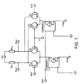
- FIG. 1 there is shown an exemplary modulator circuit diagram of the present invention.
- a suitable power supply is connected at V3v ie. 3 volts.
- the power supply V3v is connected to the output loads of the modulator circuit, the load being represented by resistors RL1 and RL2. These however may be reactive, resistive or active whichever is most suitable in the application.
- the output loads RL1 and RL2 are connected respectively to Pout and Nout which are the differential outputs of the modulator circuit.
- the signal present between Pout and Nout is the modulated radio frequency carrier.
- this differential output would be summed with the differential output of a second modulator. The summed output would then be passed to the next stage of the transmitter.
- Pout and Nout are coupled to the transistor network forming the switching means of the modulator circuit.
- the transistors Q1,2,3,4 are shown as bipolar junction transistors, but could be FETs or the like.
- Q1 and Q2 form a long tail pair as do Q3 and Q4.
- the collectors of Q1 and Q3 are connected to Pout, and the collectors of Q2 and Q4 are connected to Nout.
- REP is connected to the base of Q1 and RFN is connected to the base of Q4; RFP and RFN provide the differential inputs to the switching means, whereby the I or Q baseband signals can be injected differentially into these ports.
- Lo designates the local oscillator input port and this is connected to the bases of Q2 and Q3. This will cause the switching means to operate at twice the frequency of input.
- the emitters of each pair of long tail pairs of transistor network Q1 to Q4 are connected to a gain control means which controls the current through the transistor network.
- the gain control means comprises two current controllers labelled Current 1 and Current 2, and the level labelled Gain is an input to the current controllers whereby the current in both the pairs of long tail pairs may be increased or decreased.
- Vneg may be connected to ground or a suitable positive or negative power supply.
- the current controller operates to hold the total current through the Q1,Q2 and Q3,Q4 pairs constant. If the voltage on RFP and RFN is held constant for instance, the local oscillator signal on Lo as it becomes more positive will increase the current flow in Q2 and Q3 thus reducing the current flow in Q1 and Q4. When the local oscillator signal is lower in voltage than RFP and RFN, Q2 and Q3 will have much less current flowing in them than Q1 and Q4. When the local oscillator voltage is the same as RFP, Q1 and Q2 and also Q3 and Q4 will have the same current flowing in them. When the local oscillator voltage is greater than the voltage on RFP and RFN Q2 and Q3 will have more current flowing in them than Q3 and Q4.
- the collectors of Q1 and Q3, Q2 and Q4 are connected together.
- the current in Q1/Q4 will decrease at the same rate as the current in Q2/Q3 increases as the Lo voltage increases.
- the voltage at Pout and Nout will remain constant.
- the Local oscillator signal on Lo is larger in amplitude than Vbe i.e. 0.7 volts, it will completely switch Q2 and Q3 on and off. This is the desired mode of operation.
- the output pulses will then be of an amplitude defined solely by the amplitude of the differential signal applied between RFP and RFN and the gain defined by the current control means.
- this shows the operation of the sub-harmonic mixer with an input signal of 4.1MHz with an Lo of 2Mhz. This demonstrates its mode of operation.
- the output pulses occur, in this case, at the zero crossing points of the Lo.
- the output pulses if referenced to the first input signal have a amplitude that is proportional to the amplitude of the first input signal at that point in time.
- the ratio of the first input signal amplitude to the amplitude of the Output voltage (Gain) is determined by the current flow in the Q1,2 and Q2,3 long-tail pairs. This current flow is determined by the current control means in the emitters of the Q1,2 and Q3,4 long tail pairs.
- the present invention may be embodied in other specific forms without departing from its essential attributes.
- the switching means shown as bipolar transistors may be replaced with suitable FETs or other forms of voltage or current controlled switches. Accordingly reference should be made to the appended claims and other general statements herein rather than to the foregoing specific description as indicating the scope of invention.
Landscapes
- Transmitters (AREA)
Abstract
Description
Claims (6)
- A transmitter for a portable radio communication apparatus comprising a modulator having first port for inputting a baseband signal and a second port for inputting a local oscillator signal, and including means for rectifying the input local oscillator signal to provide a conductance waveform at a multiple of the local oscillator signal, and means for mixing the baseband signal with the conductance waveform at said multiple of the local oscillator signal frequency for up-converting the baseband signal to a radio frequency modulated carrier, the transmitter including means for controlling the gain of the modulator thereby to control the output level of the modulator.
- A transmitter according to claim 1, wherein a local oscillator signal drives the switching means at a multiple of its frequency.
- A transmitter according to claim 1 or claim 2, wherein the means for controlling the gain of the modulator comprises current control means.
- A transmitter according to any preceding claim, wherein the modulator comprises two cross-coupled pairs of switching elements, wherein a signal input modulates the switching elements at a multiple of the local oscillator frequency.
- A transmitter according to claim 4, wherein said two cross-coupled pairs of switching elements comprise two cross connected long tail pairs of bipolar transistors.
- Apparatus for a sub-harmonic mixer, comprising switching means, a first port for inputting a baseband signal to the switching means to be up-converted, and a second port for inputting a local oscillator signal to drive the switching means at an even multiple of the local oscillator frequency for up-converting the baseband signal to transmission frequency.
Applications Claiming Priority (2)
| Application Number | Priority Date | Filing Date | Title |
|---|---|---|---|
| GB9914750 | 1999-06-24 | ||
| GB9914750A GB2351404B (en) | 1999-06-24 | 1999-06-24 | A transmitter and a modulator therefor |
Publications (2)
| Publication Number | Publication Date |
|---|---|
| EP1063770A2 true EP1063770A2 (en) | 2000-12-27 |
| EP1063770A3 EP1063770A3 (en) | 2002-09-25 |
Family
ID=10855960
Family Applications (1)
| Application Number | Title | Priority Date | Filing Date |
|---|---|---|---|
| EP00305141A Withdrawn EP1063770A3 (en) | 1999-06-24 | 2000-06-16 | A transmitter and a modulator therefor |
Country Status (3)
| Country | Link |
|---|---|
| US (1) | US7107030B1 (en) |
| EP (1) | EP1063770A3 (en) |
| GB (1) | GB2351404B (en) |
Families Citing this family (5)
| Publication number | Priority date | Publication date | Assignee | Title |
|---|---|---|---|---|
| US8204469B2 (en) * | 2005-01-21 | 2012-06-19 | Nxp B.V. | Low-noise mixer |
| US7904036B2 (en) * | 2005-12-02 | 2011-03-08 | Telefonaktiebolaget Lm Ericsson (Publ) | Modulation method and apparatus |
| US7957696B2 (en) * | 2006-09-25 | 2011-06-07 | Silicon Laboratories Inc. | System and method for selecting channels for short range transmissions to broadcast receivers |
| US7656227B1 (en) | 2008-02-26 | 2010-02-02 | Pmc-Sierra, Inc. | Techniques to control amplifier gain over process, voltage, and/or temperature (PVT) variations |
| GB202007234D0 (en) * | 2020-05-15 | 2020-07-01 | Nordic Semiconductor Asa | Radio-frequency modulator apparatus |
Family Cites Families (41)
| Publication number | Priority date | Publication date | Assignee | Title |
|---|---|---|---|---|
| US3983489A (en) * | 1975-06-16 | 1976-09-28 | General Electric Company | Doubling mixer |
| CH600706A5 (en) * | 1976-09-28 | 1978-06-30 | Patelhold Patentverwertung | |
| IT1212776B (en) * | 1983-09-29 | 1989-11-30 | Ates Componenti Elettron | TRANSISTOR AMPLIFIER AND MIXER INPUT STAGE FOR A RADIO RECEIVER. |
| US5113094A (en) * | 1990-03-13 | 1992-05-12 | Wiltron Company | Method and apparatus for increasing the high frequency sensitivity response of a sampler frequency converter |
| JP2540377B2 (en) * | 1990-07-04 | 1996-10-02 | 三菱電機株式会社 | Automatic output power controller |
| US5081670A (en) * | 1991-04-02 | 1992-01-14 | Xel Communications, Inc. | Smart data station termination (DST) without active equalizers |
| JP2887993B2 (en) * | 1991-10-25 | 1999-05-10 | 日本電気株式会社 | Frequency mixer circuit |
| JP2884869B2 (en) * | 1991-12-12 | 1999-04-19 | 日本電気株式会社 | Frequency mixer circuit |
| CN1047898C (en) * | 1993-03-18 | 1999-12-29 | 东芝株式会社 | Frequency synthesizer |
| US5809410A (en) * | 1993-07-12 | 1998-09-15 | Harris Corporation | Low voltage RF amplifier and mixed with single bias block and method |
| US5552734A (en) * | 1993-10-27 | 1996-09-03 | Nec Corporation | Local oscillator frequency multiplier and mixing circuit comprising a squaring circuit |
| FI98673C (en) * | 1995-08-07 | 1997-07-25 | Nokia Telecommunications Oy | Automatic tuning of the radio transmitter |
| US6026286A (en) * | 1995-08-24 | 2000-02-15 | Nortel Networks Corporation | RF amplifier, RF mixer and RF receiver |
| JPH09238032A (en) * | 1996-02-29 | 1997-09-09 | Nec Corp | Ota and bipolar multiplier |
| JPH09270723A (en) * | 1996-03-29 | 1997-10-14 | Alps Electric Co Ltd | Ic for reception circuit for portable telephone set |
| JP3479404B2 (en) * | 1996-03-29 | 2003-12-15 | アルプス電気株式会社 | Multi-stage variable gain amplifier circuit |
| GB2313504B (en) * | 1996-05-23 | 2000-09-06 | Motorola Gmbh | Transmitter circuit and method of operation |
| JPH09321559A (en) * | 1996-05-24 | 1997-12-12 | Oki Electric Ind Co Ltd | Automatic gain control circuit |
| SE506841C2 (en) * | 1996-06-28 | 1998-02-16 | Ericsson Telefon Ab L M | Apparatus and method for phase distortion compensation |
| FR2755556A1 (en) * | 1996-11-06 | 1998-05-07 | Motorola Semiconducteurs | FREQUENCY MODULATOR, TRANSMITTER AND TRANSCEIVER INCORPORATING THE FREQUENCY MODULATOR |
| JP2954086B2 (en) * | 1997-05-16 | 1999-09-27 | 埼玉日本電気株式会社 | Mobile communication system |
| US5933767A (en) * | 1997-09-15 | 1999-08-03 | Motorola, Inc. | Apparatus and method for tuning the gain of a transmitter utilizing cartesian feedback |
| JPH1198033A (en) * | 1997-09-25 | 1999-04-09 | Circuit Design:Kk | UHF band carrier FM transmitter for wireless microphone |
| US6215986B1 (en) * | 1997-09-26 | 2001-04-10 | Nortel Networks Corporation | Reducing radio transmitter distortion |
| JP4009789B2 (en) * | 1997-10-09 | 2007-11-21 | ソニー株式会社 | Transmitter |
| US5983082A (en) * | 1997-10-31 | 1999-11-09 | Motorola, Inc. | Phase quadrature signal generator having a variable phase shift network |
| US6253092B1 (en) * | 1997-11-25 | 2001-06-26 | Uniden Financial, Inc. | Closed loop transmitter with DAC sensitivity adjusted to detector nonlinearity |
| US6317590B1 (en) * | 1997-12-23 | 2001-11-13 | Nokia Mobile Phones, Ltd. | Mixer for a receiver |
| US6259901B1 (en) * | 1998-07-03 | 2001-07-10 | Mobile Communications Tokyo Inc. | Radio-frequency power amplifier of mobile communication equipment |
| US6094571A (en) * | 1998-10-02 | 2000-07-25 | Nokia Mobile Phones Ltd. | Differential class AB mixer circuit |
| GB2344948B (en) * | 1998-12-18 | 2002-10-02 | Nokia Mobile Phones Ltd | A transceiver |
| JP3469486B2 (en) * | 1998-12-25 | 2003-11-25 | 株式会社東芝 | Variable gain circuit |
| US6205325B1 (en) * | 1998-12-31 | 2001-03-20 | Nokia Mobile Phones, Limited | Active radio frequency mixer circuit with feedback |
| US6658237B1 (en) * | 1999-03-02 | 2003-12-02 | Skyworks Solutions, Inc. | Multi-Band transceiver utilizing direct conversion receiver |
| KR100288196B1 (en) * | 1999-03-04 | 2001-04-16 | 박종섭 | Transmission control device for preventing transmitting radio frequency from oscillating in wideband wireless local loop terminal |
| US6556814B1 (en) * | 1999-07-22 | 2003-04-29 | Motorola, Inc. | Memory-based amplifier load adjust system |
| US6526265B1 (en) * | 1999-09-14 | 2003-02-25 | Skyworks Solutions, Inc. | Wireless transmitter having a modified translation loop architecture |
| US6255912B1 (en) * | 1999-09-27 | 2001-07-03 | Conexant Systems, Inc. | Phase lock loop used as up converter and for reducing phase noise of an output signal |
| JP3739614B2 (en) * | 1999-11-24 | 2006-01-25 | アルプス電気株式会社 | Transmitter for output power adjustment |
| US6633751B1 (en) * | 2000-09-21 | 2003-10-14 | Skyworks Solutions, Inc. | System for a dual feedback translation loop for power amplifier feedback control |
| US6404263B1 (en) * | 2001-07-11 | 2002-06-11 | International Business Machines Corporation | Mixer having compensation for harmonics of local oscillator signal |
-
1999
- 1999-06-24 GB GB9914750A patent/GB2351404B/en not_active Expired - Fee Related
-
2000
- 2000-06-16 EP EP00305141A patent/EP1063770A3/en not_active Withdrawn
- 2000-06-23 US US09/599,948 patent/US7107030B1/en not_active Expired - Fee Related
Also Published As
| Publication number | Publication date |
|---|---|
| EP1063770A3 (en) | 2002-09-25 |
| GB2351404B (en) | 2003-11-12 |
| GB9914750D0 (en) | 1999-08-25 |
| US7107030B1 (en) | 2006-09-12 |
| GB2351404A (en) | 2000-12-27 |
Similar Documents
| Publication | Publication Date | Title |
|---|---|---|
| Razavi | RF transmitter architectures and circuits | |
| JP3255843B2 (en) | Digital / Analog Dual Circuit in Dual Mode Radio Equipment | |
| US6397044B1 (en) | Transceiver | |
| US5392460A (en) | Dual mode radiotelephone terminal selectively operable for frequency modulated or phase modulated operation | |
| KR100356004B1 (en) | Low noise gilbert multiplier cells and quadrature modulators, and related methods | |
| US5894592A (en) | Wideband frequency synthesizer for direct conversion transceiver | |
| US7750749B2 (en) | Switching circuit, and a modulator, demodulator or mixer including such a circuit | |
| US6915117B2 (en) | Multistage modulation architecture and method in a radio | |
| CN102271000B (en) | A kind of portable computing | |
| WO2001015313A1 (en) | Local oscillator apparatus for radio frequency communication systems | |
| US9379798B2 (en) | Modulation circuit for a radio device and a method thereof | |
| GB2332796A (en) | Mixer circuits | |
| US6181212B1 (en) | Phase locked loop for generating two disparate, variable frequency signals | |
| JPH06350484A (en) | Dual mode amplifier network | |
| US7107030B1 (en) | Transmitter and a modulator therefor | |
| US4464791A (en) | All-level Rayleigh fader | |
| EP1949532B1 (en) | Switching circuit, and a modulator, demodulator or mixer including such a circuit | |
| CN101273533A (en) | EDGE transceiver architecture and related methods | |
| US8260218B2 (en) | Mixer circuit and RF transmitter using such mixer circuit | |
| US4344185A (en) | Low noise high stability FM transmitter | |
| Spears et al. | Silicon RF GCMOS performance for portable communications applications | |
| JPH07297750A (en) | Transmit / receive mixer circuit | |
| Yamaguchi et al. | A very low spurious Si-bipolar frequency multiplier | |
| CN121333346A (en) | A reconfigurable multimode multiplexed synesthetic system | |
| Bourhill et al. | Design and realisation of a novel balanced self-oscillating mixer topology |
Legal Events
| Date | Code | Title | Description |
|---|---|---|---|
| PUAI | Public reference made under article 153(3) epc to a published international application that has entered the european phase |
Free format text: ORIGINAL CODE: 0009012 |
|
| AK | Designated contracting states |
Kind code of ref document: A2 Designated state(s): AT BE CH CY DE DK ES FI FR GB GR IE IT LI LU MC NL PT SE |
|
| AX | Request for extension of the european patent |
Free format text: AL;LT;LV;MK;RO;SI |
|
| RAP1 | Party data changed (applicant data changed or rights of an application transferred) |
Owner name: NOKIA CORPORATION |
|
| PUAL | Search report despatched |
Free format text: ORIGINAL CODE: 0009013 |
|
| AK | Designated contracting states |
Kind code of ref document: A3 Designated state(s): AT BE CH CY DE DK ES FI FR GB GR IE IT LI LU MC NL PT SE |
|
| AX | Request for extension of the european patent |
Free format text: AL;LT;LV;MK;RO;SI |
|
| RIC1 | Information provided on ipc code assigned before grant |
Free format text: 7H 03G 1/00 A, 7H 03C 1/36 B, 7H 03D 7/14 B |
|
| STAA | Information on the status of an ep patent application or granted ep patent |
Free format text: STATUS: THE APPLICATION HAS BEEN WITHDRAWN |
|
| 18W | Application withdrawn |
Effective date: 20030214 |