EP1063708B1 - Photo-conductive switch having an improved semiconductor structure - Google Patents
Photo-conductive switch having an improved semiconductor structure Download PDFInfo
- Publication number
- EP1063708B1 EP1063708B1 EP00111582A EP00111582A EP1063708B1 EP 1063708 B1 EP1063708 B1 EP 1063708B1 EP 00111582 A EP00111582 A EP 00111582A EP 00111582 A EP00111582 A EP 00111582A EP 1063708 B1 EP1063708 B1 EP 1063708B1
- Authority
- EP
- European Patent Office
- Prior art keywords
- photo
- layer
- pcs
- conductive
- conductive layer
- Prior art date
- Legal status (The legal status is an assumption and is not a legal conclusion. Google has not performed a legal analysis and makes no representation as to the accuracy of the status listed.)
- Expired - Lifetime
Links
- 239000004065 semiconductor Substances 0.000 title claims description 55
- 239000000463 material Substances 0.000 claims description 116
- 239000000758 substrate Substances 0.000 claims description 72
- 238000010521 absorption reaction Methods 0.000 claims description 18
- 239000000203 mixture Substances 0.000 claims description 15
- 239000000969 carrier Substances 0.000 description 25
- 238000006243 chemical reaction Methods 0.000 description 19
- 230000005540 biological transmission Effects 0.000 description 17
- 230000004044 response Effects 0.000 description 15
- 229910001218 Gallium arsenide Inorganic materials 0.000 description 14
- 238000002296 dynamic light scattering Methods 0.000 description 14
- 229920003258 poly(methylsilmethylene) Polymers 0.000 description 14
- 238000013061 process characterization study Methods 0.000 description 14
- 238000000034 method Methods 0.000 description 10
- 229910052581 Si3N4 Inorganic materials 0.000 description 9
- 230000003287 optical effect Effects 0.000 description 9
- HQVNEWCFYHHQES-UHFFFAOYSA-N silicon nitride Chemical compound N12[Si]34N5[Si]62N3[Si]51N64 HQVNEWCFYHHQES-UHFFFAOYSA-N 0.000 description 9
- 239000011248 coating agent Substances 0.000 description 7
- 238000000576 coating method Methods 0.000 description 7
- VYPSYNLAJGMNEJ-UHFFFAOYSA-N Silicium dioxide Chemical compound O=[Si]=O VYPSYNLAJGMNEJ-UHFFFAOYSA-N 0.000 description 6
- GWEVSGVZZGPLCZ-UHFFFAOYSA-N Titan oxide Chemical compound O=[Ti]=O GWEVSGVZZGPLCZ-UHFFFAOYSA-N 0.000 description 6
- 239000002800 charge carrier Substances 0.000 description 6
- 239000010931 gold Substances 0.000 description 6
- 238000003780 insertion Methods 0.000 description 6
- 230000037431 insertion Effects 0.000 description 6
- 238000002955 isolation Methods 0.000 description 6
- 230000007423 decrease Effects 0.000 description 5
- 239000002019 doping agent Substances 0.000 description 5
- 230000000694 effects Effects 0.000 description 5
- 230000006872 improvement Effects 0.000 description 5
- 229910052710 silicon Inorganic materials 0.000 description 5
- XUIMIQQOPSSXEZ-UHFFFAOYSA-N Silicon Chemical compound [Si] XUIMIQQOPSSXEZ-UHFFFAOYSA-N 0.000 description 4
- 229910052782 aluminium Inorganic materials 0.000 description 4
- XAGFODPZIPBFFR-UHFFFAOYSA-N aluminium Chemical compound [Al] XAGFODPZIPBFFR-UHFFFAOYSA-N 0.000 description 4
- 238000005530 etching Methods 0.000 description 4
- 229910052737 gold Inorganic materials 0.000 description 4
- 230000008569 process Effects 0.000 description 4
- 230000006798 recombination Effects 0.000 description 4
- 238000005215 recombination Methods 0.000 description 4
- 238000002310 reflectometry Methods 0.000 description 4
- 239000010703 silicon Substances 0.000 description 4
- 239000010936 titanium Substances 0.000 description 4
- 229910000980 Aluminium gallium arsenide Inorganic materials 0.000 description 3
- 229910045601 alloy Inorganic materials 0.000 description 3
- 239000000956 alloy Substances 0.000 description 3
- 229910052681 coesite Inorganic materials 0.000 description 3
- 229910052906 cristobalite Inorganic materials 0.000 description 3
- 239000007772 electrode material Substances 0.000 description 3
- 238000005516 engineering process Methods 0.000 description 3
- 230000005764 inhibitory process Effects 0.000 description 3
- 238000002347 injection Methods 0.000 description 3
- 239000007924 injection Substances 0.000 description 3
- BASFCYQUMIYNBI-UHFFFAOYSA-N platinum Chemical compound [Pt] BASFCYQUMIYNBI-UHFFFAOYSA-N 0.000 description 3
- 239000000377 silicon dioxide Substances 0.000 description 3
- 229910052682 stishovite Inorganic materials 0.000 description 3
- 229910052905 tridymite Inorganic materials 0.000 description 3
- 229910052721 tungsten Inorganic materials 0.000 description 3
- 229910005542 GaSb Inorganic materials 0.000 description 2
- MHAJPDPJQMAIIY-UHFFFAOYSA-N Hydrogen peroxide Chemical compound OO MHAJPDPJQMAIIY-UHFFFAOYSA-N 0.000 description 2
- 229910002665 PbTe Inorganic materials 0.000 description 2
- 230000002745 absorbent Effects 0.000 description 2
- 239000002250 absorbent Substances 0.000 description 2
- PCHJSUWPFVWCPO-UHFFFAOYSA-N gold Chemical compound [Au] PCHJSUWPFVWCPO-UHFFFAOYSA-N 0.000 description 2
- AMGQUBHHOARCQH-UHFFFAOYSA-N indium;oxotin Chemical compound [In].[Sn]=O AMGQUBHHOARCQH-UHFFFAOYSA-N 0.000 description 2
- 238000004519 manufacturing process Methods 0.000 description 2
- 238000005259 measurement Methods 0.000 description 2
- 229910052751 metal Inorganic materials 0.000 description 2
- 239000002184 metal Substances 0.000 description 2
- 230000009467 reduction Effects 0.000 description 2
- OCGWQDWYSQAFTO-UHFFFAOYSA-N tellanylidenelead Chemical compound [Pb]=[Te] OCGWQDWYSQAFTO-UHFFFAOYSA-N 0.000 description 2
- 238000012360 testing method Methods 0.000 description 2
- 229910052719 titanium Inorganic materials 0.000 description 2
- QGZKDVFQNNGYKY-UHFFFAOYSA-O Ammonium Chemical compound [NH4+] QGZKDVFQNNGYKY-UHFFFAOYSA-O 0.000 description 1
- VHUUQVKOLVNVRT-UHFFFAOYSA-N Ammonium hydroxide Chemical compound [NH4+].[OH-] VHUUQVKOLVNVRT-UHFFFAOYSA-N 0.000 description 1
- 101100028900 Caenorhabditis elegans pcs-1 gene Proteins 0.000 description 1
- 229910000530 Gallium indium arsenide Inorganic materials 0.000 description 1
- 229910005926 GexSi1-x Inorganic materials 0.000 description 1
- RTAQQCXQSZGOHL-UHFFFAOYSA-N Titanium Chemical compound [Ti] RTAQQCXQSZGOHL-UHFFFAOYSA-N 0.000 description 1
- PNEYBMLMFCGWSK-UHFFFAOYSA-N aluminium oxide Inorganic materials [O-2].[O-2].[O-2].[Al+3].[Al+3] PNEYBMLMFCGWSK-UHFFFAOYSA-N 0.000 description 1
- 239000000908 ammonium hydroxide Substances 0.000 description 1
- 238000000137 annealing Methods 0.000 description 1
- 230000003466 anti-cipated effect Effects 0.000 description 1
- 230000009286 beneficial effect Effects 0.000 description 1
- 230000008901 benefit Effects 0.000 description 1
- 239000004020 conductor Substances 0.000 description 1
- 229910052593 corundum Inorganic materials 0.000 description 1
- 230000008878 coupling Effects 0.000 description 1
- 238000010168 coupling process Methods 0.000 description 1
- 238000005859 coupling reaction Methods 0.000 description 1
- 239000013078 crystal Substances 0.000 description 1
- 238000000151 deposition Methods 0.000 description 1
- 238000013461 design Methods 0.000 description 1
- 239000003989 dielectric material Substances 0.000 description 1
- 238000009792 diffusion process Methods 0.000 description 1
- 239000003574 free electron Substances 0.000 description 1
- 238000010438 heat treatment Methods 0.000 description 1
- 150000002500 ions Chemical group 0.000 description 1
- 238000012986 modification Methods 0.000 description 1
- 230000004048 modification Effects 0.000 description 1
- 238000001451 molecular beam epitaxy Methods 0.000 description 1
- 229910052750 molybdenum Inorganic materials 0.000 description 1
- 229910052763 palladium Inorganic materials 0.000 description 1
- 229920002120 photoresistant polymer Polymers 0.000 description 1
- 230000000704 physical effect Effects 0.000 description 1
- 229910052697 platinum Inorganic materials 0.000 description 1
- 239000000523 sample Substances 0.000 description 1
- SBIBMFFZSBJNJF-UHFFFAOYSA-N selenium;zinc Chemical compound [Se]=[Zn] SBIBMFFZSBJNJF-UHFFFAOYSA-N 0.000 description 1
- 229910052709 silver Inorganic materials 0.000 description 1
- 239000004332 silver Substances 0.000 description 1
- 239000000243 solution Substances 0.000 description 1
- 239000000126 substance Substances 0.000 description 1
- 229910001845 yogo sapphire Inorganic materials 0.000 description 1
Images


Classifications
-
- H—ELECTRICITY
- H01—ELECTRIC ELEMENTS
- H01L—SEMICONDUCTOR DEVICES NOT COVERED BY CLASS H10
- H01L31/00—Semiconductor devices sensitive to infrared radiation, light, electromagnetic radiation of shorter wavelength or corpuscular radiation and specially adapted either for the conversion of the energy of such radiation into electrical energy or for the control of electrical energy by such radiation; Processes or apparatus specially adapted for the manufacture or treatment thereof or of parts thereof; Details thereof
- H01L31/08—Semiconductor devices sensitive to infrared radiation, light, electromagnetic radiation of shorter wavelength or corpuscular radiation and specially adapted either for the conversion of the energy of such radiation into electrical energy or for the control of electrical energy by such radiation; Processes or apparatus specially adapted for the manufacture or treatment thereof or of parts thereof; Details thereof in which radiation controls flow of current through the device, e.g. photoresistors
-
- B—PERFORMING OPERATIONS; TRANSPORTING
- B82—NANOTECHNOLOGY
- B82Y—SPECIFIC USES OR APPLICATIONS OF NANOSTRUCTURES; MEASUREMENT OR ANALYSIS OF NANOSTRUCTURES; MANUFACTURE OR TREATMENT OF NANOSTRUCTURES
- B82Y20/00—Nanooptics, e.g. quantum optics or photonic crystals
-
- H—ELECTRICITY
- H01—ELECTRIC ELEMENTS
- H01L—SEMICONDUCTOR DEVICES NOT COVERED BY CLASS H10
- H01L31/00—Semiconductor devices sensitive to infrared radiation, light, electromagnetic radiation of shorter wavelength or corpuscular radiation and specially adapted either for the conversion of the energy of such radiation into electrical energy or for the control of electrical energy by such radiation; Processes or apparatus specially adapted for the manufacture or treatment thereof or of parts thereof; Details thereof
- H01L31/0248—Semiconductor devices sensitive to infrared radiation, light, electromagnetic radiation of shorter wavelength or corpuscular radiation and specially adapted either for the conversion of the energy of such radiation into electrical energy or for the control of electrical energy by such radiation; Processes or apparatus specially adapted for the manufacture or treatment thereof or of parts thereof; Details thereof characterised by their semiconductor bodies
- H01L31/0352—Semiconductor devices sensitive to infrared radiation, light, electromagnetic radiation of shorter wavelength or corpuscular radiation and specially adapted either for the conversion of the energy of such radiation into electrical energy or for the control of electrical energy by such radiation; Processes or apparatus specially adapted for the manufacture or treatment thereof or of parts thereof; Details thereof characterised by their semiconductor bodies characterised by their shape or by the shapes, relative sizes or disposition of the semiconductor regions
- H01L31/035236—Superlattices; Multiple quantum well structures
Definitions
- the invention relates generally to photo-electronic devices, and more particularly to a high performance photo-conductive switch that can be fabricated at a low cost.
- Microwave switches are being expected to perform at higher frequencies, with an improved ON to OFF ratio, a reduced insertion loss and increased isolation.
- a photo-conductive switch ( PCS ) uses light to control its electronic conductivity and therefore to modulate electronic signals passing through it.
- a photo-conductive switch has less stray electronic impedance than an equivalent electronically-controlled switch such as a transistor. Consequently, photo-conductive switches are potentially better suited for use as high-frequency and high-performance microwave switches.
- United States Patent 3,917,943 to Auston discloses a first type of PCS that is driven by an ultra-short optical pulse and is fabricated on a semiconductor substrate.
- Two gold micro-strip transmission lines separated by a narrow gap are located on the surface of a light-absorbing insulating semiconductor substrate.
- a first optical pulse directed to the substrate through the gap turns the PCS ON by generating copious electric charges on the substrate surface in the gap.
- a second optical pulse that begins during the first optical pulse and is directed to the gap generates copious electric charges in the bulk of the substrate extending down to the ground plane. This shorts the micro-strip transmission lines to ground, and switches the PCS OFF.
- the substrate is grown at a low temperature or is ion implanted to shorten the carrier lifetime to provide a very fast response. However, this also reduces the carrier mobility, which causes the PCS to have a high insertion loss.
- Figure 1 shows an embodiment of the PCS 1 disclosed by Derkits, Jr.
- the semi-insulating semiconductor substrate 10 preferably of silicon
- the ground plane electrode 11 or an ohmic contact located on its major surface 21.
- the layer 18 of a wide band-gap energy semiconductor material On the opposite major surface 22 of the substrate is located the layer 18 of a wide band-gap energy semiconductor material. Overlaying the layer 18 is the layer 19 of a graded-composition alloy semiconductor material.
- the electrodes 14 and 15 Located on surface of the layer 19 and extending over part of the major surface 22 of the substrate are the electrodes 14 and 15 separated by the gap 13. The electrodes form the ohmic contact regions 17 with the layer 19.
- the material of the layer 19 is an alloy of two semiconductor materials W and N.
- Semiconductor material W has a wide band-gap energy and semiconductor material N has a narrow band-gap energy.
- the fraction of the narrow band-gap energy semiconductor material N in the alloy increases monotonically with increasing distance from the layer 18 from a value of zero at the junction with the layer 18.
- the grooves 20 or other texturing are formed in the part of the layer 19 underlying the gap 13 to serve as charge separators.
- PCS While the PCS disclosed by Derkits offers improved performance, PCSs with further performance improvements are required to meet the requirements of present-day technology.
- US patent 5,767,560 discloses a photoelectric conversion device based on an avalanche photodiode.
- the device includes a photoelectric conversion portion having a light absorbing layer disposed between an upper and a lower charge injection inhibition layer.
- Inclined energy band gap layers are located between the light absorbing layer and the upper and lower charge injection inhibition layers, respectively.
- the upper charge injection inhibition layer is covered by a continuous upper electrodes.
- the invention provides a photo-conductive switch ( PCS ) that has a lower insertion loss and provides greater isolation than a conventional PCS.
- the insertion loss is reduced as a result of the PCS according to the invention having a smaller ON resistance R on .
- the isolation is increased as a result of the PCS according to the invention having a smaller OFF capacitance C off .
- a smaller figure of merit indicates a PCS with better performance.
- the PCS according to the invention is based on a multi-layer semiconductor structure that includes multiple heterojunctions.
- Each of the heterojunctions is a junction between a layer of a semiconductor material having a wider band-gap energy (WB material) and a layer of a semiconductor material having a narrower band-gap energy (NB material).
- the semiconductor materials forming one of the heterojunctions are doped so that they have opposite conductivity types.
- this heterojunction is formed between a layer of p-type WB material and a layer of n-type NB material, or between a layer of n-type WB material and a layer of p-type NB material.
- the PCS according to the invention comprises a three-layer semiconductor structure composed of a photo-conductive layer of NB material sandwiched between a top confinement layer and a bottom confinement layer.
- Both confinement layers are layers of WB material.
- the top confinement layer and the photo-conductive layer have opposite conductivity types.
- a first electrode and a second electrode, separated from each other by a gap, are located on the surface of the top confinement layer remote from the photo-conductive layer.
- the photo-conductive layer provides a conduction path between the electrodes when the photo-conductive layer is illuminated with incident light of an appropriate wavelength and intensity.
- the conductivity type of the photo-conductive layer is p-type and that of the top confinement layer is n-type since this combination of conductivity types provides a higher conductivity than the opposite combination.
- the double heterojunction PCS structure just described prevents charge carriers from diffusing in a direction perpendicular to the plane of the layers and enhances the efficiency with which charge carriers are generated in response to the incident light. This results in a lower ON resistance R on , and, hence, a lower insertion loss.
- the double heterojunction PCS structure just described also provides a lower OFF capacitance C off , which increases the isolation provided by the PCS according to the invention in its OFF state.
- the PCS according to the invention may additionally comprise a graded-composition layer or a chirped superlattice located between the photo-conductive layer and the top confinement layer to reduce the ON resistance R on .
- the PCS according to the invention may additionally comprise a mirror layer located to reflect incident light that passes through the photo-conductive layer back into the photo-conductive layer to reduce further the ON resistance R on
- the electrodes of the PCS according to the invention may additionally include a translucent conductive material to reduce further the ON resistance R on .
- the PCS according to the invention may additionally comprise a substrate of a substrate material that is translucent in the range of wavelengths of the incident light that are absorbed by the photo-conductive layer.
- the substrate supports at least the photo-conductive layer and the top confinement layer.
- the incident light passes through the translucent substrate to illuminate the photo-conductive layer. Since the incident light is not partially obstructed by the electrodes, the ON resistance R on is reduced.
- the PCS according to the invention may alternatively comprise an opaque substrate that supports the double heterojunction PCS structure, and the substrate may define a through-hole that admits the incident light to illuminate the photo-conductive layer. Since the incident light is not partially obstructed by the electrodes, the ON resistance R on is also reduced.
- the invention is based on the inventors recognizing the following four problems associated with prior-art PCSs and generating effective solutions to these problems.
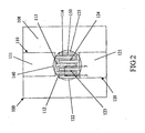
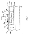
- FIG. 2 and Figure 3 illustrate a first, basic embodiment 100 of a PCS according to the invention.
- the PCS 100 is composed of the bottom confinement layer 104 of WB material, i.e., a semiconductor material having a wide band-gap energy; the photo-conductive layer 106 of NB material, i.e., a semiconductor material having a narrow band-gap energy; and the top confinement layer 108 of WB material.
- the photo-conductive layer is sandwiched between the bottom confinement layer and the top confinement layer.
- the terminal 110 is composed of the electrodes 112, 113 and 114 coupled to the bonding pad 111.
- the terminal 120 is composed of the electrodes 122, 123, 124 and 125 coupled to the bonding pad 121.
- the electrodes of the terminal 110 are separated from the electrodes of the terminal 120 by a narrow gap.
- the bottom confinement layer 104 is shown in Figure 3 as a layer of WB material grown or deposited on the semiconductor substrate 102. This enables commonly-available, low-cost semiconductor materials to be used for the substrate. Such materials are not usually WB materials. However, if the semiconductor material of the substrate is a WB material, such as InP, the bottom confinement layer may be integral with the substrate, and no separate bottom confinement layer is necessary.
- the photo-conductive layer 106 and the top confinement layer 108 are successively grown or deposited on the bottom confinement layer.
- the conductivity type of the WB material of the top confinement layer 108 is opposite to that of the NB material of the photo-conductive layer 106.
- the conductivity of the WB material of the top confinement layer is n-type and that of the NB material of the photo-conductive layer 106 is p-type, although the conductivity types of the WB and NB materials may be reversed.
- the WB material of the bottom confinement layer 104 may be the same as the WB material of the top confinement layer 108. Alternatively, different WB materials may be used for the top and bottom confinement layers.
- the conductivity type of the WB material of the bottom confinement layer may be of the same as that of the photo-conductive layer 106, or may be the opposite of that of the photo-conductive layer, or the WB material of the bottom confinement layer may be undoped.
- the top confinement layer 108 covers the surface of the photo-conductive layer and substantially reduces the number of dangling bonds present at the surface of the photo-conductive layer.
- the top confinement layer increases the number of carriers extant in the photo-conductive layer in response to a given intensity of the incident light.
- FIG. 3 also shows the portions 108A, 108B and 108C of the top confinement layer that are not covered by the electrodes 112 and 123.
- the top surface of the portions 108A, 108B and 108C of the top confinement layer has a surface state energy that is strongly pinned at several times the thermal energy ( kT , where k is Boltzmann's constant and T is the absolute temperature) in the band gap of the WB material. As a result, these portions are depleted through the entire thickness of the top confinement layer.
- the portions 108A-108C of the top confinement layer 108 are depleted through the thickness of the layer, no conduction path exists in the top confinement layer between the terminals 110 and 120. Moreover, in the absence of incident light, the two back-to-back p-n junctions that exist between the top confinement layer and the photo-conductive layer 106 block conduction between the terminals through the photo-conductive layer 106. Conduction between the terminals occurs only when the PCS 100 is illuminated with the incident light 142, which causes carriers to be generated in the photo-conductive layer.
- the electrodes 112-114 forming part of the terminal 110 are interdigitated with the electrodes 122-125 forming part of the terminal 120.
- the shape and location of the electrodes are preferably optimized to minimize the ON resistance R on between the terminals 110 and 120 when the PCS 100 is illuminated by the incident light 142.
- Figure 2 shows at 140 the substantially circular area on the top surface of the PCS 100 that is illuminated by the incident light 142.
- the beam of incident light is shaped so that the area 140 covers most of the region where the electrodes are interdigitated.
- the electrodes 112-114 and 122-125 When conventional opaque metal electrodes are used as the electrodes 112-114 and 122-125, the electrodes reflect or absorb the fraction of the incident light 142 that illuminates the electrodes. This fraction of the incident light does not reach the photo-conductive layer 106 and generate carriers. In cases in which the area of the area 140 is limited, a trade off may be made between the fraction of the area 140 that is covered by the electrodes, and the remainder of the area 140 through which the incident light 142 can reach the photo-conductive layer 106 and generate carriers.
- the preferred characteristics of the confinement layers 104 and 108 are as follows:
- the preferred characteristics of the photo-conductive layer 106 are as follows:
- the properties of the NB material of the photo-conductive layer 106 determine the lifetime of the carriers generated in response to the incident light 142. As noted above, it is generally desirable to increase the lifetime of the carriers. However, too long a carrier lifetime impairs the switching speed of the PCS. Consequently, the carrier lifetime should be shorter than the desired switching time of the PCS 100. Otherwise, the carriers generated in response to the incident light will continue to exist a significant time after the incident light 142 ceases to illuminate the PCS 100. The remaining carriers increase the conductance of the PCS in its OFF state, which decreases the isolation provided by the PCS in its OFF state. In many applications, a switching time of about 1ms is acceptable. Even NB materials, such as silicon, that have extremely long carrier lifetimes can easily provide such a switching speed. NB materials such as GaAs can be used when higher switching speeds are required.
- Illuminating the PCS 100 with the incident light 142 sets the PCS to its ON state.
- the PCS 100 is most commonly used in RF and microwave systems, which typically have a characteristic impedance of 50 ⁇ .
- the ON resistance R on of a PCS for use in systems with a 50 ⁇ characteristic impedance is acceptably small if it is small compared with 50 ⁇ , i.e., R on « 50 ⁇ .
- measures that decrease the ON resistance to a level that is small compared with 50 ⁇ provide a useful improvement in the performance of the PCS.
- the incident light 142 should be converted to carriers with a high overall conversion efficiency.
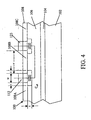
- Figure 4 shows the PCS 100 in its OFF state in the absence of the incident light 142.
- the impedance of the PCS in its OFF state is the impedance of the parallel combination of the ohmic resistance of the PCS in its OFF state and the reactance 1/2 ⁇ f ⁇ C off of the OFF capacitance C off , where f is the frequency of the signal being switched by the PCS.
- the PCS according to the invention is most commonly used in RF and microwave systems, which typically have a characteristic impedance of 50 ⁇ . At RF and microwave frequencies, the dominant element in determining the impedance of the parallel combination is the reactance of the OFF capacitance C off .
- the OFF capacitance C off of a PCS for use in a system with a characteristic impedance of 50 ⁇ is acceptably low if its reactance is large compared with 50 ⁇ , i.e., 1/2 ⁇ f ⁇ C off » 50 ⁇ .
- the main contributors to the OFF capacitance C off are (1) the capacitance of the depletion layer between the photo-conductive layer 106 and the top confinement layer 108, (2) the capacitance of the depletion layer created by dangling bonds in the top confinement layer 108, and (3) the capacitance of the depletion layer between the photo-conductive layer 106 and the bottom confinement layer 104.
- C off ⁇ ⁇ l ⁇ ( w + 2 t ) 2 t
- t 2 ⁇ ⁇ n ⁇ ⁇ p ⁇ ( ⁇ i ⁇ V ) q ⁇ p n ( p ⁇ p + n ⁇ n )
- Examples of combinations of materials that can be used for the substrate, the confinement layers and the photo-conductive layer in the PCSs disclosed in this disclosure are shown in Table 1.
- the materials of the photo-conductive layer 106 and at least the top confinement layer 108 are doped with appropriate dopants to define their conductivity types.
- Photo-conductive layer 1 GaAs Al y Ga 1-y As (0.02 ⁇ y ⁇ 1.0) Al x Ga 1-x As (x ⁇ y) 2 GaAs (Al y Ga 1-y ) 0.5 In 0.5 P (0.0 ⁇ y ⁇ 1.0) Al x Ga 1-x As (0.0 ⁇ x ⁇ 0.5) 3 GaAs Al y Ga 1-y As (0.0 ⁇ y ⁇ 1.0) In x Ga 1-x As (0.01 ⁇ x ⁇ 0.3) 4 InP (Al y Ga 1-x ) 0.5 In 0.5 As (0.01 ⁇ x ⁇ 1.0) In 0.5 Ga 0.5 As 5 InP (Al x Ga 1-x ) 0.5 In 0.5 AS (0.01 ⁇ x ⁇ 1.0) GaAs 0.5 Sb 0.5 6 SiC or Al 2 O 3 Al x Ga 1-x N (0.01 ⁇ x ⁇ 1.0) GaN 7 Si Si Ge x Si 1-x (0.05 ⁇ x ⁇ 1.0) 8 Si or SiC SiC Si 9 GaAs or ZnSe Zny M
- the bottom confinement layer 104 and the top confinement layer 108 can be layers of different materials. In such event, the material of the top confinement layer is listed in Table 1.
- combinations 1-4 and 7 are favored because they have a high electron mobility and long carrier lifetimes and can be made using available mature epitaxial growth and process technologies.
- the substrate material in combinations 4 and 5 is InP, which is a WB material.
- the lower confinement layer 104 can be integral with the substrate 102, and the photo-conductive layer 106 can be deposited directly on the surface of the substrate.
- the substrate material in combination 7 is silicon, which is a WB material.
- the lower confinement layer can be integral with the substrate, and the photo-conductive layer can be deposited directly on the surface of the substrate.
- the incident light 142 may be generated using any suitable light source.
- a miniature light source such as a semiconductor light-emitting device is preferred.
- a semiconductor laser is most preferred for use in PCSs for switching microwave signals with switching speeds in the microsecond range.
- Semiconductor lasers are small in size, operate at a speed high enough to obtain the desired switching speeds and are low in cost.
- Semiconductor lasers are available that can emit light in the wavelength range from 0.40 to 1.55 ⁇ m. Most of the above combinations will operate in response to a laser generating light in this wavelength range.
- the wavelength of the incident light must lie in the range of wavelengths that is transmitted by the material of the confinement layer through which the light passes to the photo-conductive layer and that is absorbed by the material of the photo-conductive layer.
- the ON resistance of the PCS 100 just described can be further reduced by locating a graded-composition layer or a chirped super lattice multi-layered film at the heterojunction between the top confinement layer 108 and the photo-conductive layer 106.
- the band-gap energy of the graded composition layer changes progressively through the thickness of the layer, while that of the chirped super-lattice multi-layered film changes in steps through the thickness of the film to simulate the effect of a continuously graded-composition layer.
- MBE molecular-beam epitaxy
- the confinement layers may have composition ratios different from those just described. However, the aluminum fraction in the top confinement layer 208 should preferably be less than 0.25.
- the density of deep levels or DX centers in the top confinement layer drastically increases, as described by M. Tachikawa et al., 23 JPN. J. APPL. PHYS., 1594 (1984).
- the DX centers dramatically reduce the free electron concentration in the top confinement layer, which significantly increases the ON resistance R on .
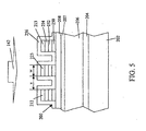
- the graded-composition layers 207 and 250 formed of n-type semiconductor material doped at n 3 ⁇ 10 17 cm -3 , i.e., the same doping concentration as the top confinement layer 208, are epitaxially grown before and after, respectively, the top confinement layer 208 is grown.
- the graded-composition layer 207 is 30nm thick and composed of n-type Al x Ga 1-x As in which the value of the aluminum fraction x progressively increases from zero at the photo-conductive layer 206 to 0.23 at the top confinement layer 208.
- the graded-composition layer 250 is 30nm thick and is composed of n-type Al x Ga 1-x As in which the value of the aluminum fraction x progressively decreases from 0.23 at the top confinement layer 208 to zero at the GaAs cap layer 252.
- the n-type In 0.5 Ga 0.5 As contact layer 254, which is 20 nm thick and is heavily doped at n 2 ⁇ 10 19 cm -3 , is grown on the cap layer 252.
- the contact layer supports the metal electrodes 212-214 and 222-225 that form a non-alloyed contact with the contact layer. Of the electrodes 212-214 and 222-225, only the electrodes 212, 213 and 223 are shown in Figure 5.
- the electrodes may be composed of layers of titanium, platinum and gold with a total thickness of 300 nm.
- the cap layer 252 and the contact layer 254 reduce the contact resistance between the graded-composition layer 250 and the electrodes 212-214 and 222-225. This reduction in the contact resistance is achieved without performing any heat treatment, such as annealing.
- This method and structure for reducing contact resistance are based on the method of manufacturing heterojunction transistors (HBT) described by F. Ren et al. in 28 ELECTRON. LETT., 1150 (1992).
- HBT heterojunction transistors
- the PCS 200 is fabricated by successively growing the layers 204, 206, 207, 208, 250, 252 and 254 and then depositing a Ti/Pt/Au electrode layer in which the electrodes 212-214 and 222-225 will be defined.
- the electrode layer is then patterned to define the individual electrodes.
- the semiconductor materials of the graded-composition layer 250, the cap layer 252 and the contact layer 254 between the electrodes are then etched away. The etch stops at the top confinement layer 208.
- the electrodes may be used as an etch mask that defines the portions of the layers 250, 252 and 254 that are not etched away.
- the silicon nitride (Si 3 N 4 ) anti-reflection coating 256 is deposited on the top surface of the PCS 100, including the electrodes 212-214 and 222-225 and the exposed surface of the top confinement layer 208.
- the thickness of the anti-reflection coating is 100 nm. The anti-reflection coating prevents or reduces reflection of the incident light that would otherwise occur due to the large difference in refractive index between the AlGaAs of the top confinement layer 208 and the ambient, such as air.
- the PCS 200 is switched ON by illuminating it with a beam of incident light generated by a semiconductor laser.
- the wavelength of the incident light is chosen to be one at which the energy per photon is below the band edge of the WB material of the confinement layer through which the incident light reaches the photo-conductive layer 206, i.e., the top confinement layer 208 in this example, to minimize absorption by the confinement layer.
- the wavelength of the incident light is also chosen to be one at which the energy per photon is above the band edge of the NB material of the photo-conductive layer 206 to maximize absorption of the incident light by the photo-conductive layer.
- the incident light had a wavelength of about 0.78 ⁇ m.
- the beam of incident light has a substantially-circular cross section about 30 ⁇ m in diameter.
- a commercially-available semiconductor laser can be used to generate the incident light 142 so that the miniature PCS 200 can be manufactured at low cost.
- the semiconductor path ON resistance is the resistance of the conduction path through the top confinement layer 208 and the photo-conductive layer 206 when the PCS 200 is illuminated by the incident light.
- Figure 6 is a graph showing of the variation of the semiconductor path ON resistance with the power of the laser that generates the incident light.
- Test samples having the characteristics just described were fabricated.
- the test samples were illuminated with incident light generated by a 5 mW laser and measurements of their ON resistance were made.
- the ON resistance R on measured between the terminals 110 and 120 was in the range of three to five ohms. However, it was determined that an abnormally high contact resistance R c between the terminals 110 and 120 and the top confinement layer 208 accounted for most of the ON resistance. Additional measurements showed that the semiconductor path ON resistance R s ( on ) was about one ohm. It is anticipated that the contact resistance R c of additional samples currently in fabrication will be less than the semiconductor path ON resistance R s ( on ) . Such samples will have an ON resistance that is acceptable for use as a microwave switch.
- the two main elements that lower the conversion efficiency ⁇ are ⁇ s , the electrode transmission factor, and ⁇ a , the absorptance of the photo-conductive layer 106.
- the low value of the electrode transmission factor ⁇ s indicates that the electrodes 212-214 and 222-225 prevent a substantial fraction of the incident light from reaching the photo-conductive layer 206.
- the absorptance ⁇ a of the photo-conductive layer 206 having a low value indicates that a substantial fraction of the incident light that reaches the photo-conductive layer passes through the photo-conductive layer without being absorbed.
- the main element of the OFF capacitance C off of the PCS 200 is the capacitance of the depletion layer between the photo-conductive layer 206 and the top confinement layer 208, and depends on the doping concentration in the photo-conductive layer.
- Figure 7 shows the OFF capacitance plotted against the doping concentration of the photo-conductive layer. The OFF capacitance C off increases as the doping concentration increases, so a lower doping concentration reduces the OFF capacitance C off .
- the doping concentration of the photo-conductive layer be in the range from 1 ⁇ 10 15 cm -3 to 1 ⁇ 10 17 cm -3 . Doping concentrations in this range provide an acceptable trade-off between the OFF capacitance C off and the punch-through voltage.
- the OFF capacitance C off needs to be no smaller than that which has a reactance at the frequency f of the signal being switched that is large compared with 50 ⁇ , i.e., 1/2 ⁇ f. C off » 50 ⁇ .
- the PCS 200 depicted in Figure 5 has an OFF capacitance C off of 60 fF, and a figure of merit R on ⁇ C off of 0.06 ⁇ pF. This is smaller, and therefore better, than that of conventional high-frequency switches.
- FIG 8 shows a third embodiment 300 of a PCS according to the invention in which the conversion efficiency is further increased.
- the structure of the PCS 300 is similar to that of the PCS 200 shown in Figure 5. Elements of the PCS 300 that correspond to elements of the PCS 200 are indicated by the same reference numerals and will not be described again here.
- the main factors that lower the overall conversion efficiency ⁇ of the PCS 200 are ⁇ s , the electrode transmission factor, and ⁇ ⁇ , the absorptance of the photo-conductive layer 106.
- the bottom confinement layer is structured as the mirror layer 304.
- the mirror layer effectively increases the absorptance ⁇ a of the photo-conductive layer by reflecting the portion of the incident light that passes through the photo-conductive layer 206 without being absorbed back into the photo-conductive layer.
- the mirror layer 304 is a distributed Bragg reflector composed of multiple pairs of sub-layers of semiconductor material.
- An exemplary pair of sub-layers is shown at 360.
- the pair of sub-layers 360 is composed of the 64 nm-thick Al 0.3 G 0.7 As sub layer 362 and the 73 nm-thick AlAs sub layer 364.
- the materials of the sub-layers constituting the mirror layer 304 were doped n-type, the mirror layer was composed of 10 pairs of sub-layers, and the reflectivity of the mirror layer was about 90 %.
- the reflectivity of the bottom confinement layer 204 of the PCS 200 is about 0.08 %.
- the mirror layer 304 effectively increases the absorptance ⁇ a of the photo-conductive layer 206 to 98 % in the PCS 300, compared with 60 % in the PCS 200. This increases the overall conversion efficiency ⁇ to 66%, and reduces the semiconductor path ON resistance R s ( on ) to two-thirds of that of the PCS 200.
- the main factors that lower the overall conversion efficiency ⁇ of the PCS 200 are ⁇ s' the electrode transmission factor, and ⁇ a , the absorptance of the photo-conductive layer 206.
- the electrode transmission factor is usually equal to the fraction of the light reception area 140 ( Figure 2) not covered by the electrodes 212-214 and 222-225 because the electrodes are conventionally opaque and reflective.
- the electrodes absorb or reflect the fraction of the incident light 142 that falls on them, which prevents this fraction of the incident light from passing through the top confinement layer 208 to the photo-conductive layer 206.
- the electrode transmission factor can be increased to close to 100%, and the conversion efficiency of the PCS can be increased yet further, by configuring the PCS according to the invention so that the electrodes prevent little, if any, of the incident light from reaching the photo-conductive layer.
- the PCS 300 shown in Figure 8 can be configured so that the electrodes 212-214 and 222-225 (of which only 212, 223 and 213 are shown) prevent only a small fraction of the incident light 142 from reaching the photo-conductive layer 206 by fabricating the electrodes from a translucent material.
- a translucent material include, for example, indium-tin oxide (ITO) and a thin layer of silver.
- the PCS can be configured so that its electrodes prevent none of the incident light from passing to the photo-conductive layer. This is done by configuring the PCS so that the incident light reaches the photo-conductive layer through the bottom confinement layer, where there are no electrodes to absorb or reflect the incident light.
- FIG 9 shows a fourth embodiment 400 of a PCS according to the invention in which the conversion efficiency is increased yet further.
- the structure of the PCS 400 is similar to that of the PCS 200 shown in Figure 5. Elements of the PCS 400 that correspond to elements of the PCS 200 are indicated by the same reference numerals and will not be described again here.
- the overall conversion efficiency ⁇ of the PCS 400 is increased by both increasing the electrode transmission factor ⁇ s and by effectively increasing the absorptance ⁇ a of the photo-conductive layer.
- the substrate 402 is a wafer of a material that is translucent in the range of wavelengths of the incident light 142 that are absorbed by the photo-conductive layer 406. This enables the PCS 400 to receive the incident light through the substrate where there are no electrodes to absorb or reflect part the incident light. This increases the electrode transmission factor ⁇ s to close to 100 %.
- the PCS 400 includes the mirror layer 456 located over the surface of the PCS remote from the substrate. The mirror layer effectively increases the absorptance ⁇ a of the photo-conductive layer 406 by reflecting the incident light that passes through the photo-conductive layer without being absorbed back into the photo-conductive layer.
- the substrate 402 is a wafer of InP
- the photo-conductive layer 406 is a layer of InGaAs
- the top confinement layer 408 is a layer of (Al x Ga 1-x ) 0.5 In 0.5 As.
- the substrate material is a WB material, so the bottom confinement layer 404 is integral with the substrate in the example shown.
- the substrate material is translucent in the range of wavelengths of the incident light 142 that are absorbed by the photo-conductive layer 406.
- Other materials may be used as the substrate 402, the photo-conductive layer 406 and the top confinement layer 408.
- the bottom confinement layer 404 may be a separate layer of WB material deposited or grown on the substrate 402 instead of being integral with the substrate.
- the surface 480 of the substrate remote from the electrodes, of which only the electrodes 212, 213 and 223 are shown, is coated with the anti-reflection coating 462, a 100nm-thick layer of silicon nitride (Si 3 N 4 ), to reduce reflection of the incident light 142 by the surface 480 of the substrate.
- the PCS 400 is mounted in a way that allows the incident light to illuminate the surface 480 of the substrate 402.
- flip-chip bonding techniques may be used to mount the PCS on a suitable header (not shown) with the substrate oriented to receive the incident light 142 from the laser or LED that generates the incident light.
- the incident light passes through the substrate to reach the photo-conductive layer 406. Since there are no electrodes located in the path of the incident light, the electrode transmission factor ⁇ s is close to 100%.
- the PCS 400 is fabricated by first forming a structure substantially similar to that of the PCS 200. However, different materials are used for the substrate 402, the confinement layers 404 and 408 and the photo-conductive layer 406, as described above. Also, the Si 3 N 4 anti-reflection coating 256 is omitted and the mirror layer 456 is instead located on the surface of the PCS remote from the substrate 402. In this example, the mirror layer 456 is a distributed Bragg reflector composed of multiple pairs of sub-layers of dielectric materials. An exemplary pair of sub-layers is shown at 460. The pair of sub-layers 460 is composed of a 147nm-thick layer of SiO 2 and a 99 nm-thick layer of TiO 2 .
- the improvement in the overall conversion efficiency ⁇ results in a semiconductor path ON resistance R s ( on ) of about one-half of that of the PCS 200.
- Similar results are predicted for an embodiment based on the PCS 300 shown in Figure 8 in which the electrodes 212-214 and 222-225 are fabricated from a translucent electrode material indium tin oxide (ITO) instead of a conventional opaque electrode material.
- ITO indium tin oxide
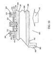
- FIG. 10 shows a fifth embodiment 500 of a PCS according to the invention in which the overall conversion efficiency ⁇ is similar to that of the PCS 400 just described. Elements of the PCS 500 that correspond to elements of the PCSs 200 and 400 described above are indicated by the same reference numerals and will not be described again here.
- the overall conversion efficiency ⁇ of the PCS 500 is increased by both increasing the electrode transmission factor ⁇ s and by effectively increasing the absorptance ⁇ a of the photo-conductive layer.
- the PCS 500 includes the through hole 560 etched through the thickness of the substrate 502 to allow the incident light to illuminate the bottom confinement layer 204, and to pass through the bottom confinement layer to reach the photo-conductive layer 206.
- the PCS 500 also includes the mirror layer 456 over the surface of the PCS remote from the substrate 502, which effectively increases the absorptance ⁇ a of the photo-conductive layer 206, as described above.
- the substrate 502 is a wafer of GaAs
- the photo-conductive layer 206 is a layer of Al x Ga 1-x As
- the confinement layers 204 and 208 are layers of Al y Ga 1-y AS, where x ⁇ y.
- the substrate material is absorbent in the range of wavelengths of the incident light 142 that are absorbed by the photo-conductive layer.
- the substrate material is also absorbent in the range of wavelengths of the incident light that are absorbed by the photo-conductive layer in other combinations of materials from which the PCS may be fabricated.
- the through hole 560 is also beneficial to etch the through hole 560 through the thickness of the substrate even in embodiments of the PCS in which the substrate material is nominally translucent in the range of wavelengths of the incident light that are absorbed by the photo-conductive layer, since the through-hole reduces absorption of the incident light that would otherwise occur as a result of the incident light passing through the thickness of the substrate.
- Etching the through-hole 560 presents the problem of controlling the etch process so that the through-hole extends through the entire thickness of the substrate 502 but does not remove all or part of the bottom confinement layer 204. This is especially difficult because the thickness of the bottom confinement layer is very small compared with the thickness of the substrate (less than 0.1 ⁇ m compared with more than one hundred ⁇ m).
- the inventors have solved this problem by using a material for the bottom confinement layer that is etched by a given echant at a substantially slower rate than the material of the substrate. This enables the bottom confinement layer to act as an etch stop for the etching process.
- the bottom confinement layer 204 may be a layer of AlGaAs, which serves as an effective etch stop when etching GaAs.
- This method for forming the through-hole 560 is based on the method described by H. Tanobe et al. in 31 JPN. J. APPL. PHYS.,1597 (1992) for fabricating a surface-emitting laser, and will not be described in further detail here.
- the PCS 500 is fabricated by a method based on that described above for fabricating the PCS 400, except that the materials of the substrate 502, the photo-conductive layer 206 and top confinement layer 208 are different. Also, in the example shown, a separate layer of WB material is deposited on the substrate to form the bottom confinement layer 204, as in the PCS 200. After the mirror layer 456 has been deposited, and the part of the mirror layer that overlies the bonding pads 111 and 121 ( Figure 2) has been etched off, the surface 580 of the substrate 502 remote from the mirror layer 456 is masked by a layer of photoresist except for the area in which the through-hole 560 is to be located.
- the PCS is then etched using a chemical etchant that etches GaAs at a considerably faster rate than AlGaAs.
- Etchants of the ammonium system are known in the art that provide an etch rate ratio of more than 10:1.
- One example of such an etchant is a mixture of hydrogen peroxide and ammonium hydroxide. Using such an etchant enables the bottom confinement layer 204 to act as an etch stop when the through-hole is etched.
- the anti-reflection coating 562 a 100nm-thick layer of silicon nitride (Si 3 N 4 ), is deposited on the surface 580 of the substrate, on the side-walls of the though-hole and on the exposed surface of the bottom confinement layer 204.
- the improvement in the overall conversion efficiency ⁇ results in a semiconductor path ON resistance R s ( on ) of about one-half of that of the PCS 200.
Description
- The invention relates generally to photo-electronic devices, and more particularly to a high performance photo-conductive switch that can be fabricated at a low cost.
- Microwave switches are being expected to perform at higher frequencies, with an improved ON to OFF ratio, a reduced insertion loss and increased isolation. A photo-conductive switch (PCS) uses light to control its electronic conductivity and therefore to modulate electronic signals passing through it. A photo-conductive switch has less stray electronic impedance than an equivalent electronically-controlled switch such as a transistor. Consequently, photo-conductive switches are potentially better suited for use as high-frequency and high-performance microwave switches.
- United States Patent 3,917,943 to Auston discloses a first type of PCS that is driven by an ultra-short optical pulse and is fabricated on a semiconductor substrate. Two gold micro-strip transmission lines separated by a narrow gap are located on the surface of a light-absorbing insulating semiconductor substrate. A first optical pulse directed to the substrate through the gap turns the PCS ON by generating copious electric charges on the substrate surface in the gap. A second optical pulse that begins during the first optical pulse and is directed to the gap generates copious electric charges in the bulk of the substrate extending down to the ground plane. This shorts the micro-strip transmission lines to ground, and switches the PCS OFF. The substrate is grown at a low temperature or is ion implanted to shorten the carrier lifetime to provide a very fast response. However, this also reduces the carrier mobility, which causes the PCS to have a high insertion loss.
- United States Patent 4,755,663 to Derkits, Jr. indicates that a disadvantage of the Auston PCS is that the electrical impulse created by the optical pulse is dominated by carrier recombination, rather than carrier transport. Derkits discloses a PCS in which the portion of the substrate constituting the gap includes a region composed of a textured-surface, graded-composition photosensitive semiconductor material. Illuminating the gap with a beam of light of sufficient intensity to generate charge carriers at the surface of the photosensitive semiconductor material causes the PCS to conduct.
- Figure 1 shows an embodiment of the
PCS 1 disclosed by Derkits, Jr. In this, thesemi-insulating semiconductor substrate 10, preferably of silicon, has theground plane electrode 11 or an ohmic contact located on itsmajor surface 21. On the oppositemajor surface 22 of the substrate is located thelayer 18 of a wide band-gap energy semiconductor material. Overlaying thelayer 18 is thelayer 19 of a graded-composition alloy semiconductor material. Located on surface of thelayer 19 and extending over part of themajor surface 22 of the substrate are theelectrodes gap 13. The electrodes form theohmic contact regions 17 with thelayer 19. - The material of the
layer 19 is an alloy of two semiconductor materials W and N. Semiconductor material W has a wide band-gap energy and semiconductor material N has a narrow band-gap energy. The fraction of the narrow band-gap energy semiconductor material N in the alloy increases monotonically with increasing distance from thelayer 18 from a value of zero at the junction with thelayer 18. Thegrooves 20 or other texturing are formed in the part of thelayer 19 underlying thegap 13 to serve as charge separators. - Light falling on the
layer 19 through thegap 13 creates charge carriers that provide electrical conduction between theelectrodes layer 19 where the narrow band-gap energy material is predominant. In this region, thegrooves 20 separate the charge carriers and prevent further conduction between the electrode segments. - While the PCS disclosed by Derkits offers improved performance, PCSs with further performance improvements are required to meet the requirements of present-day technology.
- US patent 5,767,560 discloses a photoelectric conversion device based on an avalanche photodiode. The device includes a photoelectric conversion portion having a light absorbing layer disposed between an upper and a lower charge injection inhibition layer. Inclined energy band gap layers are located between the light absorbing layer and the upper and lower charge injection inhibition layers, respectively. The upper charge injection inhibition layer is covered by a continuous upper electrodes.
- The invention provides a photo-conductive switch (PCS) that has a lower insertion loss and provides greater isolation than a conventional PCS. The insertion loss is reduced as a result of the PCS according to the invention having a smaller ON resistance R on . The isolation is increased as a result of the PCS according to the invention having a smaller OFF capacitance C off . Thus, the PCS according to the invention has a smaller figure of merit F = R on × C off than a conventional PCS. A smaller figure of merit indicates a PCS with better performance.
- The PCS according to the invention is based on a multi-layer semiconductor structure that includes multiple heterojunctions. Each of the heterojunctions is a junction between a layer of a semiconductor material having a wider band-gap energy (WB material) and a layer of a semiconductor material having a narrower band-gap energy (NB material). The semiconductor materials forming one of the heterojunctions are doped so that they have opposite conductivity types. Thus, this heterojunction is formed between a layer of p-type WB material and a layer of n-type NB material, or between a layer of n-type WB material and a layer of p-type NB material.
- The PCS according to the invention comprises a three-layer semiconductor structure composed of a photo-conductive layer of NB material sandwiched between a top confinement layer and a bottom confinement layer.
- Both confinement layers are layers of WB material. The top confinement layer and the photo-conductive layer have opposite conductivity types. A first electrode and a second electrode, separated from each other by a gap, are located on the surface of the top confinement layer remote from the photo-conductive layer. The photo-conductive layer provides a conduction path between the electrodes when the photo-conductive layer is illuminated with incident light of an appropriate wavelength and intensity.
- Preferably, the conductivity type of the photo-conductive layer is p-type and that of the top confinement layer is n-type since this combination of conductivity types provides a higher conductivity than the opposite combination.
- The double heterojunction PCS structure just described prevents charge carriers from diffusing in a direction perpendicular to the plane of the layers and enhances the efficiency with which charge carriers are generated in response to the incident light. This results in a lower ON resistance R on , and, hence, a lower insertion loss.
- The double heterojunction PCS structure just described also provides a lower OFF capacitance C off , which increases the isolation provided by the PCS according to the invention in its OFF state.
- The PCS according to the invention may additionally comprise a graded-composition layer or a chirped superlattice located between the photo-conductive layer and the top confinement layer to reduce the ON resistance R on .
- The PCS according to the invention may additionally comprise a mirror layer located to reflect incident light that passes through the photo-conductive layer back into the photo-conductive layer to reduce further the ON resistance R on
- The electrodes of the PCS according to the invention may additionally include a translucent conductive material to reduce further the ON resistance R on .
- The PCS according to the invention may additionally comprise a substrate of a substrate material that is translucent in the range of wavelengths of the incident light that are absorbed by the photo-conductive layer. The substrate supports at least the photo-conductive layer and the top confinement layer. The incident light passes through the translucent substrate to illuminate the photo-conductive layer. Since the incident light is not partially obstructed by the electrodes, the ON resistance R on is reduced.
- The PCS according to the invention may alternatively comprise an opaque substrate that supports the double heterojunction PCS structure, and the substrate may define a through-hole that admits the incident light to illuminate the photo-conductive layer. Since the incident light is not partially obstructed by the electrodes, the ON resistance R on is also reduced.
-
- Figure 1 is a cross sectional view of a prior-art photo-conductive switch (PCS).
- Figure 2 is a plan view of a first embodiment of a PCS according to the invention in its conducting state.
- Figure 3 is a cross-sectional view of the PCS according to the invention taken along the line 3-3 in Figure 2.
- Figure 4 is a cross-sectional view of part of the first embodiment of the PCS according to the invention in its non-conducting state.
- Figure 5 is a cross-sectional view of part of a second embodiment of a PCS according to the invention in its conducting state.
- Figure 6 is a graph showing the variation of the semiconductor path ON resistance R s(on) with the power of the laser generating the incident light in the embodiment of the PCS shown in Figure 5. The semiconductor path ON resistance is the ON resistance of the conductive path through the top confinement layer and the photo-conductive layer of the double heterojunction PCS structure.
- Figure 7 is a graph showing the variation of the OFF capacitance C off with the dopant concentration in the photo-conductive layer in the embodiment of the PCS shown in Figure 5.
- Figure 8 is a cross-sectional view of part of a third embodiment of a PCS according to the invention in its conducting state.
- Figure 9 is a cross-sectional view of part of a fourth embodiment of a PCS according to the invention in its conducting state.
- Figure 10 is a cross-sectional view of part of a fifth embodiment of a PCS according to the invention in its conducting state.
- The invention is based on the inventors recognizing the following four problems associated with prior-art PCSs and generating effective solutions to these problems.
- 1. Prior-art PCSs are constructed from materials grown at a low temperature and therefore have a high insertion loss because of the low carrier mobility of such materials.
- 2. The structure of prior-art PCSs does not allow the carriers generated in response to the incident light to contribute efficiently to conduction between the electrodes. For example, prior-art PCSs lack a structure that confines the carriers generated in response to the incident light to a specific location. Instead, the structure of prior-art PCSs allows the carriers to diffuse away from where they are formed so that fewer carriers are available to provide conduction between the electrodes
- 3. In prior-art PCSs, a portion of the carriers generated in response to the incident light reaches the electrodes, where recombination takes place. This recombination results in regions of a low carrier density, where the resistivity is higher. This results in a high ON resistance R on . High resistance regions are also found in n-i-n devices.
- 4. Dangling bonds at the surfaces of the semiconductor layers in prior-art PCSs form traps where the carriers generated in response to the incident light can recombine. This reduces the efficiency with which carriers are generated in response to the incident light.
- Figure 2 and Figure 3 illustrate a first,
basic embodiment 100 of a PCS according to the invention. ThePCS 100 is composed of thebottom confinement layer 104 of WB material, i.e., a semiconductor material having a wide band-gap energy; the photo-conductive layer 106 of NB material, i.e., a semiconductor material having a narrow band-gap energy; and thetop confinement layer 108 of WB material. The photo-conductive layer is sandwiched between the bottom confinement layer and the top confinement layer. Located on the exposed surface of thetop confinement layer 108 are theterminals electrodes bonding pad 111. The terminal 120 is composed of theelectrodes bonding pad 121. The electrodes of the terminal 110 are separated from the electrodes of the terminal 120 by a narrow gap. - The
bottom confinement layer 104 is shown in Figure 3 as a layer of WB material grown or deposited on thesemiconductor substrate 102. This enables commonly-available, low-cost semiconductor materials to be used for the substrate. Such materials are not usually WB materials. However, if the semiconductor material of the substrate is a WB material, such as InP, the bottom confinement layer may be integral with the substrate, and no separate bottom confinement layer is necessary. The photo-conductive layer 106 and thetop confinement layer 108 are successively grown or deposited on the bottom confinement layer. - The conductivity type of the WB material of the
top confinement layer 108 is opposite to that of the NB material of the photo-conductive layer 106. Preferably, the conductivity of the WB material of the top confinement layer is n-type and that of the NB material of the photo-conductive layer 106 is p-type, although the conductivity types of the WB and NB materials may be reversed. - The WB material of the
bottom confinement layer 104 may be the same as the WB material of thetop confinement layer 108. Alternatively, different WB materials may be used for the top and bottom confinement layers. The conductivity type of the WB material of the bottom confinement layer may be of the same as that of the photo-conductive layer 106, or may be the opposite of that of the photo-conductive layer, or the WB material of the bottom confinement layer may be undoped. - Absent the
top confinement layer 108, dangling bonds would exist at the surface of the photo-conductive layer 106. Such dangling bonds create surface states that trap the carriers generated in response to theincident light 142 and promote recombination of the carriers. In thePCS 100, thetop confinement layer 108 covers the surface of the photo-conductive layer and substantially reduces the number of dangling bonds present at the surface of the photo-conductive layer. Thus, the top confinement layer increases the number of carriers extant in the photo-conductive layer in response to a given intensity of the incident light. - Only those portions of the
top confinement layer 108, such as theportions terminals portions electrodes portions - When the
portions 108A-108C of thetop confinement layer 108 are depleted through the thickness of the layer, no conduction path exists in the top confinement layer between theterminals conductive layer 106 block conduction between the terminals through the photo-conductive layer 106. Conduction between the terminals occurs only when thePCS 100 is illuminated with theincident light 142, which causes carriers to be generated in the photo-conductive layer. - The electrodes 112-114 forming part of the terminal 110 are interdigitated with the electrodes 122-125 forming part of the terminal 120. The shape and location of the electrodes are preferably optimized to minimize the ON resistance R on between the
terminals PCS 100 is illuminated by theincident light 142. Figure 2 shows at 140 the substantially circular area on the top surface of thePCS 100 that is illuminated by theincident light 142. The beam of incident light is shaped so that thearea 140 covers most of the region where the electrodes are interdigitated. - When conventional opaque metal electrodes are used as the electrodes 112-114 and 122-125, the electrodes reflect or absorb the fraction of the incident light 142 that illuminates the electrodes. This fraction of the incident light does not reach the photo-
conductive layer 106 and generate carriers. In cases in which the area of thearea 140 is limited, a trade off may be made between the fraction of thearea 140 that is covered by the electrodes, and the remainder of thearea 140 through which theincident light 142 can reach the photo-conductive layer 106 and generate carriers. - The preferred characteristics of the confinement layers 104 and 108 are as follows:
- The band-gap energies of the WB materials of the confinement layers 104 and 108 should preferably be more than 25meV greater than the band-gap energy of the NB material of the photo-
conductive layer 106 to prevent the carriers generated in the photo-conductive layer in response to the incident light 142 from diffusing into the confinement layers. The band-gap energy difference of 25 meV corresponds to thermal energy at room temperature. - The confinement layer through which the incident light reaches the photo-
conductive layer 106, e.g., thetop confinement layer 108 in the embodiment shown in Figures 2 and 3, should be as thin as possible and the WB material of the confinement layer should be highly transparent at the wavelength of the incident light 142 to maximize the transmission of the incident light through the confinement layer to the photo-conductive layer 106. In other words, the product of the thickness t c of the confinement layer and the absorption coefficient α c of the WB material of the confinement layer should be significantly smaller than unity., i.e., t c α c « 1. Tunnelling effects set a practical limit to the minimum thickness of the confinement layer. Consequently, the absorption coefficient of the confinement layer through which the incident light reaches the photo-conductive layer is preferably less than 100 cm-1. - The WB material of the
top confinement layer 108 should have a high electron mobility to provide a high conductivity. A high conductivity reduces the resistance of the conduction paths through thetop confinement layer 108 from the electrodes 112-114 and 122-125 to the photo-conductive layer 106. - The WB material of the
top confinement layer 108 should have a high doping concentration to provide the top confinement layer with a high conductivity. However, too high a doping concentration would prevent the top confinement layer of a given thickness from being fully depleted. Reducing the thickness of the top confinement layer to enable the layer to be fully depleted increases tunnelling effects. Thus, the optimum doping concentration of the WB material of the top confinement layer involves a trade-off between these conflicting requirements. A doping concentration of the order of 1 × 1017cm-3 is an acceptable compromise. - The preferred characteristics of the photo-
conductive layer 106 are as follows: - The photo-
conductive layer 106 should be as thick as can be practically fabricated, and the NB material of the photo-conductive layer should have as high an absorption coefficient as possible at the wavelength of theincident light 142. These characteristics enable the photo-conductive layer to absorb as much of the incident light 142 as possible, and therefore generate as many carriers as possible in response to the incident light. In other words, the product of the thickness d of the photo-conductive layer and the absorption coefficient α p of the NB material of the photo-conductive layer at the wavelength of the incident light should be greater than about unity, i.e., dα p >~ 1. Process limitations on the maximum thickness of photo-conductive layer make it desirable for the absorption coefficient of the NB material of the photo-conductive layer to be greater than 1000cm-1 at the wavelength of the incident light. The wavelength of the incident light should be chosen so that the photon energy of the incident light is greater than the band edge energy of the NB material of the photo-conductive layer to maximize the absorption coefficient. - The NB material of the photo-
conductive layer 106 should have a high carrier mobility to provide the photo-conductive layer 106 with a high conductivity. A high conductivity reduces the resistance of the photo-conductive layer to reduce the ON resistance R on . - The lifetime of carriers in the NB material of the photo-
conductive layer 106 should be long so that the carriers can contribute to transmission of the signal through thePCS 100. - The NB material of the photo-
conductive layer 106 should have a doping concentration of less than 1×1017cm-3 to reduce the OFF capacitance C off . - The properties of the NB material of the photo-
conductive layer 106 determine the lifetime of the carriers generated in response to theincident light 142. As noted above, it is generally desirable to increase the lifetime of the carriers. However, too long a carrier lifetime impairs the switching speed of the PCS. Consequently, the carrier lifetime should be shorter than the desired switching time of thePCS 100. Otherwise, the carriers generated in response to the incident light will continue to exist a significant time after the incident light 142 ceases to illuminate thePCS 100. The remaining carriers increase the conductance of the PCS in its OFF state, which decreases the isolation provided by the PCS in its OFF state. In many applications, a switching time of about 1ms is acceptable. Even NB materials, such as silicon, that have extremely long carrier lifetimes can easily provide such a switching speed. NB materials such as GaAs can be used when higher switching speeds are required. - Illuminating the
PCS 100 with the incident light 142 sets the PCS to its ON state. ThePCS 100 is most commonly used in RF and microwave systems, which typically have a characteristic impedance of 50 Ω. The ON resistance R on of a PCS for use in systems with a 50 Ω characteristic impedance is acceptably small if it is small compared with 50 Ω, i.e., R on « 50 Ω. Thus, for a given intensity of the incident light 142 in such PCSs, measures that decrease the ON resistance to a level that is small compared with 50 Ω provide a useful improvement in the performance of the PCS. However, measures that, for the same intensity of the incident light, reduce the ON resistance below the level that is small compared with 50 Ω have a negligible effect on the performance of the PCS. Nevertheless, such measures are worth implementing because they enable the ON resistance to be small compared with 50 Ω at a lower intensity of the incident light. This enables the incident light to be generated using a simpler, lower-cost light source that generates less heat. Such a light source generally has improved lifetime and reliability, and consumes less power. Thus, the measures to be described below for reducing the ON resistance R on of thePCS 100 can additionally or alternatively be used to reduce the intensity of the incident light at which the ON resistance is small compared with 50 Ω. - In the ON state of the
PCS 100, as shown in Figure 3, the ON resistance R on of the PCS is determined by the following equations:
where:

- R on is the ON resistance of the PCS measured between the
terminals - R s(on) is the semiconductor path ON resistance, i.e., the resistance of the conduction path through the
top confinement layer 108 and the photo-conductive layer 106, - R c is the resistance of the contacts between the
terminals top confinement layer 108, - q is the unit charge,
- µ is the carrier mobility,
- n is the population of carriers generated in response to the
incident light 142, - w is the width of the electrodes,
- v is the distance between the electrodes,
- l is the length of the perimeter of the electrodes subject to irradiation by the incident light, as indicated by the
broken line 150 in Figure 2, - d is the thickness of the photo-
conductive layer 106, - h is Planck's constant,
- ν is the frequency of the incident light,
- τ is the carrier lifetime,
- D is the diffusion constant of the carriers,
- P is the intensity of the incident light,
- α p is the optical absorption coefficient of the photo-conductive layer, and
- A and B are constants.
- From the above equation, it can be seen that increasing P, the intensity of the incident light, and selecting semiconductor materials that have higher values of the carrier mobility µ, the carrier lifetime τ and the optical absorption coefficient α p reduces the ON resistance R on . The optical absorption coefficient α p increases as the frequency v of the incident light increases, so it is preferable to employ incident light having a short wavelength. A lens is preferably used to focus the incident light into a small volume of the photo-
conductive layer 106 to increase the intensity P. This is especially useful in embodiments of the PCS for use at higher frequencies in which the dimensions of the PCS should be small. - To reduce the ON resistance R on , the
incident light 142 should be converted to carriers with a high overall conversion efficiency. The overall conversion efficiency η is given by:
- η c is the coupling efficiency determining the fraction of the
incident light 142 actually received by thelight reception area 140 of the PCS 100 (95% in this embodiment), - η s is the electrode transmission factor, i.e., the fraction of the incident light not absorbed or reflected by the electrodes 112-114 and 122-125. In the
PCS 100, the electrode transmission factor is approximately equal to the fraction of thelight reception area 140 not covered by the electrodes, - η r is the fraction of the incident light transmitted through the confinement layer to the photo-
conductive layer 106, - η a is the absorptance the photo-
conductive layer 106, and - η i is the internal quantum efficiency with which the photo-conductive layer converts light into carriers.
- Figure 4 shows the
PCS 100 in its OFF state in the absence of theincident light 142. The impedance of the PCS in its OFF state is the impedance of the parallel combination of the ohmic resistance of the PCS in its OFF state and thereactance 1/2πf·C off of the OFF capacitance C off , where f is the frequency of the signal being switched by the PCS. As noted above, the PCS according to the invention is most commonly used in RF and microwave systems, which typically have a characteristic impedance of 50 Ω. At RF and microwave frequencies, the dominant element in determining the impedance of the parallel combination is the reactance of the OFF capacitance C off . The OFF capacitance C off of a PCS for use in a system with a characteristic impedance of 50 Ω is acceptably low if its reactance is large compared with 50 Ω, i.e., 1/2πf·C off » 50 Ω. - . In PCSs for use in applications having a characteristic impedance of 50 Ω, measures that decrease the OFF capacitance C off to one having a reactance at a given frequency that is large compared with 50 Ω provide a useful improvement in the performance of the PCS. However, measures that further decrease the OFF capacitance have a negligible effect on the performance of the PCS. Nevertheless, such measures are worth pursuing because they enable the OFF capacitance to have a reactance that is large compared with 50 Ω at yet higher frequencies. This extends the range of applications in which the PCS according to the invention can be used. Thus, the measures to be described below for reducing the OFF capacitance C off can additionally or alternatively be used to provide an OFF capacitance that has a reactance that is large compared with 50 Ω at higher operating frequencies.
- The main contributors to the OFF capacitance C off are (1) the capacitance of the depletion layer between the photo-
conductive layer 106 and thetop confinement layer 108, (2) the capacitance of the depletion layer created by dangling bonds in thetop confinement layer 108, and (3) the capacitance of the depletion layer between the photo-conductive layer 106 and thebottom confinement layer 104. Of these, the capacitance of the depletion layer between the photo-conductive layer 106 and thetop confinement layer 108 predominates, and the OFF capacitance C off can be approximately determined using the equation:
where:
- t is the thickness of the depletion layer,
- εn is the permittivity of the confinement layer,
- ε p is the permittivity of the photo-conductive layer,
- l is the length of the perimeter of the electrodes, as indicated by the
broken line 150 in Figure 2 - w is the width of the electrodes,
- n and p are the dopant concentrations of the
top confinement layer 108 and the photo-conductive layer 106 respectively, - Φ i is the built-in potential, and
- V is an applied voltage (V=0 in this example).
- It can be seen that reducing the dopant concentration p in the photo-
conductive layer 106 reduces the OFF capacitance C off . However, the minimum dopant concentration is subject to practical limitations, as will be discussed below. - The above equations enable the design of the
PCS 100 to be optimized to obtain a small figure of merit R on × C off . This figure of merit is one important measure for a high performance PCS. - Examples of combinations of materials that can be used for the substrate, the confinement layers and the photo-conductive layer in the PCSs disclosed in this disclosure are shown in Table 1. The materials of the photo-
conductive layer 106 and at least thetop confinement layer 108 are doped with appropriate dopants to define their conductivity types.Table 1 Substrate Confinement layers Photo- conductive layer 1 GaAs AlyGa1-yAs (0.02<y<1.0) AlxGa1-xAs (x<y) 2 GaAs (Aly Ga1-y)0.5 In0.5 P (0.0≤y<1.0) Alx Ga1-x As (0.0≤x<0.5) 3 GaAs AlyGa1-yAs (0.0<y<1.0) InxGa1-xAs (0.01<x<0.3) 4 InP (AlyGa1-x)0.5In0.5As (0.01 <x< 1.0) In0.5Ga0.5 As 5 InP (Alx Ga1-x)0.5In0.5AS (0.01 <x< 1.0) GaAs0.5Sb0.5 6 SiC or Al2O3 AlxGa1-xN (0.01<x<1.0) GaN 7 Si Si GexSi1-x (0.05<x<1.0) 8 Si or SiC SiC Si 9 GaAs or ZnSe Zny Mg1-ySzSe1-z (0.0<y<1.0 and 0.0<z<1.0) ZnSxSe1-x (0.0<x<1.0) 10 GaSb Alx Ga1-x Sb (0.01 <x< 1.0) GaSb 11 PbTe PbxCd1-x Te (0.01<x<1.0) PbTe - As noted above, the
bottom confinement layer 104 and thetop confinement layer 108 can be layers of different materials. In such event, the material of the top confinement layer is listed in Table 1. - One advantage of the combinations of materials listed in Table 1 is that they minimize the lattice mismatch between adjacent layers and therefore have a longer carrier lifetime than combinations having a larger lattice mismatch.
- Of the above combinations, combinations 1-4 and 7 are favored because they have a high electron mobility and long carrier lifetimes and can be made using available mature epitaxial growth and process technologies.
- The substrate material in combinations 4 and 5 is InP, which is a WB material. In PCSs fabricated using combination 4 or combination 5, the
lower confinement layer 104 can be integral with thesubstrate 102, and the photo-conductive layer 106 can be deposited directly on the surface of the substrate. Also, the substrate material in combination 7 is silicon, which is a WB material. In a PCS with a silicon substrate, the lower confinement layer can be integral with the substrate, and the photo-conductive layer can be deposited directly on the surface of the substrate. - The
incident light 142 may be generated using any suitable light source. A miniature light source such as a semiconductor light-emitting device is preferred. A semiconductor laser is most preferred for use in PCSs for switching microwave signals with switching speeds in the microsecond range. Semiconductor lasers are small in size, operate at a speed high enough to obtain the desired switching speeds and are low in cost. Semiconductor lasers are available that can emit light in the wavelength range from 0.40 to 1.55 µm. Most of the above combinations will operate in response to a laser generating light in this wavelength range. For a given combination of materials, the wavelength of the incident light must lie in the range of wavelengths that is transmitted by the material of the confinement layer through which the light passes to the photo-conductive layer and that is absorbed by the material of the photo-conductive layer. - The ON resistance of the
PCS 100 just described can be further reduced by locating a graded-composition layer or a chirped super lattice multi-layered film at the heterojunction between thetop confinement layer 108 and the photo-conductive layer 106. The band-gap energy of the graded composition layer changes progressively through the thickness of the layer, while that of the chirped super-lattice multi-layered film changes in steps through the thickness of the film to simulate the effect of a continuously graded-composition layer. - A
second embodiment 200 of a PCS according to the invention will now be described with reference to Figure 5. - The
PCS 200 is composed of the undoped, 70 nm-thick Al0.3Ga0.7 Asbottom confinement layer 204, the p-type GaAs photo-conductive layer 206 (1.70 µm thick and doped at p=2×1016cm-3) and the n-type Al0.23G0.77As top confinement layer 208 (70 nm thick and doped at n=3 × 1017 cm-3). These layers are successively grown on thesemi-insulating GaAs substrate 202 using molecular-beam epitaxy (MBE) or another suitable epitaxial growth technique. The confinement layers may have composition ratios different from those just described. However, the aluminum fraction in thetop confinement layer 208 should preferably be less than 0.25. If the aluminum fraction in the top confinement layer exceeds 0.25, the density of deep levels or DX centers in the top confinement layer drastically increases, as described by M. Tachikawa et al., 23 JPN. J. APPL. PHYS., 1594 (1984). The DX centers dramatically reduce the free electron concentration in the top confinement layer, which significantly increases the ON resistance R on. - The graded-
composition layers top confinement layer 208, are epitaxially grown before and after, respectively, thetop confinement layer 208 is grown. - The graded-
composition layer 207 is 30nm thick and composed of n-type Al x Ga1-xAs in which the value of the aluminum fraction x progressively increases from zero at the photo-conductive layer 206 to 0.23 at thetop confinement layer 208. - Similarly, the graded-
composition layer 250 is 30nm thick and is composed of n-type Al x Ga1-x As in which the value of the aluminum fraction x progressively decreases from 0.23 at thetop confinement layer 208 to zero at theGaAs cap layer 252. - The n-type
GaAs cap layer 252, which has a thickness of 200 nm and is doped at n=5×1018 cm-3, is grown on the graded-composition layer 250. The n-type In0.5Ga0.5Ascontact layer 254, which is 20 nm thick and is heavily doped at n=2×1019 cm-3, is grown on thecap layer 252. The contact layer supports the metal electrodes 212-214 and 222-225 that form a non-alloyed contact with the contact layer. Of the electrodes 212-214 and 222-225, only theelectrodes cap layer 252 and thecontact layer 254 reduce the contact resistance between the graded-composition layer 250 and the electrodes 212-214 and 222-225. This reduction in the contact resistance is achieved without performing any heat treatment, such as annealing. This method and structure for reducing contact resistance are based on the method of manufacturing heterojunction transistors (HBT) described by F. Ren et al. in 28 ELECTRON. LETT., 1150 (1992). - The
PCS 200 is fabricated by successively growing thelayers composition layer 250, thecap layer 252 and thecontact layer 254 between the electrodes are then etched away. The etch stops at thetop confinement layer 208. The electrodes may be used as an etch mask that defines the portions of thelayers - Finally, the silicon nitride (Si3N4)
anti-reflection coating 256 is deposited on the top surface of thePCS 100, including the electrodes 212-214 and 222-225 and the exposed surface of thetop confinement layer 208. The thickness of the anti-reflection coating is 100 nm. The anti-reflection coating prevents or reduces reflection of the incident light that would otherwise occur due to the large difference in refractive index between the AlGaAs of thetop confinement layer 208 and the ambient, such as air. - The
PCS 200 is switched ON by illuminating it with a beam of incident light generated by a semiconductor laser. The wavelength of the incident light is chosen to be one at which the energy per photon is below the band edge of the WB material of the confinement layer through which the incident light reaches the photo-conductive layer 206, i.e., thetop confinement layer 208 in this example, to minimize absorption by the confinement layer. The wavelength of the incident light is also chosen to be one at which the energy per photon is above the band edge of the NB material of the photo-conductive layer 206 to maximize absorption of the incident light by the photo-conductive layer. In the example just described, the incident light had a wavelength of about 0.78 µm. The beam of incident light has a substantially-circular cross section about 30 µm in diameter. A commercially-available semiconductor laser can be used to generate the incident light 142 so that theminiature PCS 200 can be manufactured at low cost. - The characteristics of the beam of incident light 142, the physical properties of GaAs and such device parameters as the optical absorption coefficient of the photo-
conductive layer 206 α p =9,000 cm-1, the carrier lifetime τ=10 ns, the carrier mobility µ=6,300 cm2/Vs, the electrode width w=3 µm and the inter-electrode spacing v=2 µm were used to calculate the semiconductor path ON resistance R s(on) of thePCS 200. The semiconductor path ON resistance is the resistance of the conduction path through thetop confinement layer 208 and the photo-conductive layer 206 when thePCS 200 is illuminated by the incident light. Figure 6 is a graph showing of the variation of the semiconductor path ON resistance with the power of the laser that generates the incident light. In this exemplary embodiment, the thickness d of the photo-conductive layer 206 is at least 1.7 µm, which is greater than the absorption length α p -1=1.1 µm. - Test samples having the characteristics just described were fabricated. The test samples were illuminated with incident light generated by a 5 mW laser and measurements of their ON resistance were made. The ON resistance R on measured between the
terminals terminals top confinement layer 208 accounted for most of the ON resistance. Additional measurements showed that the semiconductor path ON resistance R s(on) was about one ohm. It is anticipated that the contact resistance R c of additional samples currently in fabrication will be less than the semiconductor path ON resistance R s(on). Such samples will have an ON resistance that is acceptable for use as a microwave switch. - The overall conversion efficiency of the
PCS 200 is η=η c × η s × η r × η a × η i = 95% × 60% × 99% × 75% × 95% = 40%, where η c = 95%, η s = 60%, η r = 99%, η a = 75% and η i = 95%. The two main elements that lower the conversion efficiency η are η s , the electrode transmission factor, and η a , the absorptance of the photo-conductive layer 106. The low value of the electrode transmission factor η s indicates that the electrodes 212-214 and 222-225 prevent a substantial fraction of the incident light from reaching the photo-conductive layer 206. The absorptance η a of the photo-conductive layer 206 having a low value indicates that a substantial fraction of the incident light that reaches the photo-conductive layer passes through the photo-conductive layer without being absorbed. - The main element of the OFF capacitance C off of the
PCS 200 is the capacitance of the depletion layer between the photo-conductive layer 206 and thetop confinement layer 208, and depends on the doping concentration in the photo-conductive layer. Figure 7 shows the OFF capacitance plotted against the doping concentration of the photo-conductive layer. The OFF capacitance C off increases as the doping concentration increases, so a lower doping concentration reduces the OFF capacitance C off . - However, an excessive reduction in the doping concentration causes an excessive increase in the thickness of the depletion layers. This reduces the punch-through voltage of the
PCS 200. If the amplitude of the signal being switched by the PCS exceeds the punch-through voltage, the impedance of the PCS falls to a small value, and the PCS no longer provides isolation in its OFF state. Moreover, with current crystal growth technology, it is difficult to control the doping concentration at low doping levels. Consequently, it is preferred that the doping concentration of the photo-conductive layer be in the range from 1× 1015 cm-3 to 1 × 1017 cm-3. Doping concentrations in this range provide an acceptable trade-off between the OFF capacitance C off and the punch-through voltage. Reducing the area of the electrodes 212-214 and 222-225 also reduces the OFF capacitance C off . As noted above, in embodiments of the PCS for use in systems with a characteristic impedance of 50 Ω, the OFF capacitance C off needs to be no smaller than that which has a reactance at the frequency f of the signal being switched that is large compared with 50 Ω, i.e., 1/2πf.C off » 50 Ω. - The
PCS 200 depicted in Figure 5 has an OFF capacitance C off of 60 fF, and a figure of merit R on × C off of 0.06 ΩpF. This is smaller, and therefore better, than that of conventional high-frequency switches. - Figure 8 shows a
third embodiment 300 of a PCS according to the invention in which the conversion efficiency is further increased. The structure of thePCS 300 is similar to that of thePCS 200 shown in Figure 5. Elements of thePCS 300 that correspond to elements of thePCS 200 are indicated by the same reference numerals and will not be described again here. As noted above, the main factors that lower the overall conversion efficiency η of thePCS 200 are η s , the electrode transmission factor, and η α , the absorptance of the photo-conductive layer 106. In thePCS 300, the bottom confinement layer is structured as themirror layer 304. The mirror layer effectively increases the absorptance η a of the photo-conductive layer by reflecting the portion of the incident light that passes through the photo-conductive layer 206 without being absorbed back into the photo-conductive layer. - In the example shown, the
mirror layer 304 is a distributed Bragg reflector composed of multiple pairs of sub-layers of semiconductor material. An exemplary pair of sub-layers is shown at 360. The pair ofsub-layers 360 is composed of the 64 nm-thick Al0.3G0.7Assub layer 362 and the 73 nm-thick AlAssub layer 364. The thickness t m of each sub-layer is equal to an integral odd multiple of one-fourth of the wavelength λ of the incident light 142 in the material of the sub-layer, i.e., t m =mλ/4n, where: - m is an odd integer,
- λ is the wavelength of the incident light 142 in free space, and
- n is the refractive index of the material of the sub-layer at the wavelength λ.
- In one practical embodiment of the
PCS 300, the materials of the sub-layers constituting themirror layer 304 were doped n-type, the mirror layer was composed of 10 pairs of sub-layers, and the reflectivity of the mirror layer was about 90 %. The reflectivity of thebottom confinement layer 204 of thePCS 200 is about 0.08 %. - The
mirror layer 304 effectively increases the absorptance η a of the photo-conductive layer 206 to 98 % in thePCS 300, compared with 60 % in thePCS 200. This increases the overall conversion efficiency η to 66%, and reduces the semiconductor path ON resistance R s(on) to two-thirds of that of thePCS 200. - As noted above, the main factors that lower the overall conversion efficiency η of the
PCS 200 are ηs' the electrode transmission factor, and η a , the absorptance of the photo-conductive layer 206. The electrode transmission factor is usually equal to the fraction of the light reception area 140 (Figure 2) not covered by the electrodes 212-214 and 222-225 because the electrodes are conventionally opaque and reflective. The electrodes absorb or reflect the fraction of the incident light 142 that falls on them, which prevents this fraction of the incident light from passing through thetop confinement layer 208 to the photo-conductive layer 206. The electrode transmission factor can be increased to close to 100%, and the conversion efficiency of the PCS can be increased yet further, by configuring the PCS according to the invention so that the electrodes prevent little, if any, of the incident light from reaching the photo-conductive layer. - For example, the
PCS 300 shown in Figure 8 can be configured so that the electrodes 212-214 and 222-225 (of which only 212, 223 and 213 are shown) prevent only a small fraction of the incident light 142 from reaching the photo-conductive layer 206 by fabricating the electrodes from a translucent material. A number of suitable conductive translucent materials are known in the art and include, for example, indium-tin oxide (ITO) and a thin layer of silver. - Alternatively, the PCS can be configured so that its electrodes prevent none of the incident light from passing to the photo-conductive layer. This is done by configuring the PCS so that the incident light reaches the photo-conductive layer through the bottom confinement layer, where there are no electrodes to absorb or reflect the incident light.
- Figure 9 shows a
fourth embodiment 400 of a PCS according to the invention in which the conversion efficiency is increased yet further. The structure of thePCS 400 is similar to that of thePCS 200 shown in Figure 5. Elements of thePCS 400 that correspond to elements of thePCS 200 are indicated by the same reference numerals and will not be described again here. The overall conversion efficiency η of thePCS 400 is increased by both increasing the electrode transmission factor η s and by effectively increasing the absorptance η a of the photo-conductive layer. - In the
PCS 400, thesubstrate 402 is a wafer of a material that is translucent in the range of wavelengths of the incident light 142 that are absorbed by the photo-conductive layer 406. This enables thePCS 400 to receive the incident light through the substrate where there are no electrodes to absorb or reflect part the incident light. This increases the electrode transmission factor η s to close to 100 %. Also, thePCS 400 includes themirror layer 456 located over the surface of the PCS remote from the substrate. The mirror layer effectively increases the absorptance η a of the photo-conductive layer 406 by reflecting the incident light that passes through the photo-conductive layer without being absorbed back into the photo-conductive layer. - In the example shown, the
substrate 402 is a wafer of InP, the photo-conductive layer 406 is a layer of InGaAs and the top confinement layer 408 is a layer of (Alx Ga1-x)0.5In0.5As. The substrate material is a WB material, so thebottom confinement layer 404 is integral with the substrate in the example shown. Moreover, as noted above, the substrate material is translucent in the range of wavelengths of the incident light 142 that are absorbed by the photo-conductive layer 406. Other materials may be used as thesubstrate 402, the photo-conductive layer 406 and the top confinement layer 408. Moreover, thebottom confinement layer 404 may be a separate layer of WB material deposited or grown on thesubstrate 402 instead of being integral with the substrate. - The
surface 480 of the substrate remote from the electrodes, of which only theelectrodes anti-reflection coating 462, a 100nm-thick layer of silicon nitride (Si3N4), to reduce reflection of theincident light 142 by thesurface 480 of the substrate. - The
PCS 400 is mounted in a way that allows the incident light to illuminate thesurface 480 of thesubstrate 402. For example, flip-chip bonding techniques may be used to mount the PCS on a suitable header (not shown) with the substrate oriented to receive the incident light 142 from the laser or LED that generates the incident light. The incident light passes through the substrate to reach the photo-conductive layer 406. Since there are no electrodes located in the path of the incident light, the electrode transmission factor ηs is close to 100%. - The
PCS 400 is fabricated by first forming a structure substantially similar to that of thePCS 200. However, different materials are used for thesubstrate 402, the confinement layers 404 and 408 and the photo-conductive layer 406, as described above. Also, the Si3N4anti-reflection coating 256 is omitted and themirror layer 456 is instead located on the surface of the PCS remote from thesubstrate 402. In this example, themirror layer 456 is a distributed Bragg reflector composed of multiple pairs of sub-layers of dielectric materials. An exemplary pair of sub-layers is shown at 460. The pair ofsub-layers 460 is composed of a 147nm-thick layer of SiO2 and a 99 nm-thick layer of TiO2. These thicknesses correspond to one-fourth of the wavelength of the incident light 142 in the respective materials, as described above. Due to the large difference in refractive index between the SiO2 and TiO2 of the sub-layers (1.45 for SiO2 and 2.15 for TiO2), only three pair of sub-layers are required to provide a reflectivity of about 90%. Such a reflectivity increases the effective absorptance η a of the photo-conductive layer 406 to about 98%. After the mirror layer has been deposited, the part of themirror layer 456 that overlies thebonding pads 111 and 121 (Figure 2) is etched off. Finally, theanti-reflection coating 462, a 100nm-thick layer of silicon nitride (Si3N4), is deposited on thesurface 480 of the substrate. - The overall conversion efficiency of the
PCS 400 is predicted to be η = η c × η s × η r × η a × η i = 95% × 100% × 99% × 98% × 95% = 88%. The improvement in the overall conversion efficiency η results in a semiconductor path ON resistance R s(on) of about one-half of that of thePCS 200. Similar results are predicted for an embodiment based on thePCS 300 shown in Figure 8 in which the electrodes 212-214 and 222-225 are fabricated from a translucent electrode material indium tin oxide (ITO) instead of a conventional opaque electrode material. - Figure 10 shows a
fifth embodiment 500 of a PCS according to the invention in which the overall conversion efficiency η is similar to that of thePCS 400 just described. Elements of thePCS 500 that correspond to elements of thePCSs PCS 400, the overall conversion efficiency η of thePCS 500 is increased by both increasing the electrode transmission factor ηs and by effectively increasing the absorptance η a of the photo-conductive layer. ThePCS 500 includes the throughhole 560 etched through the thickness of thesubstrate 502 to allow the incident light to illuminate thebottom confinement layer 204, and to pass through the bottom confinement layer to reach the photo-conductive layer 206. Since there are no electrodes located in the path of the incident light, this increases the electrode transmission factor η s to close to 100 % while enabling the material of the substrate to be opaque in the range of wavelengths of the incident light that are absorbed by the photo-conductive layer. ThePCS 500 also includes themirror layer 456 over the surface of the PCS remote from thesubstrate 502, which effectively increases the absorptance η a of the photo-conductive layer 206, as described above. - In the example shown, the
substrate 502 is a wafer of GaAs, the photo-conductive layer 206 is a layer of AlxGa1-xAs and the confinement layers 204 and 208 are layers of AlyGa1-yAS, where x<y. The substrate material is absorbent in the range of wavelengths of the incident light 142 that are absorbed by the photo-conductive layer. The substrate material is also absorbent in the range of wavelengths of the incident light that are absorbed by the photo-conductive layer in other combinations of materials from which the PCS may be fabricated. It is also beneficial to etch the throughhole 560 through the thickness of the substrate even in embodiments of the PCS in which the substrate material is nominally translucent in the range of wavelengths of the incident light that are absorbed by the photo-conductive layer, since the through-hole reduces absorption of the incident light that would otherwise occur as a result of the incident light passing through the thickness of the substrate. - Etching the through-
hole 560 presents the problem of controlling the etch process so that the through-hole extends through the entire thickness of thesubstrate 502 but does not remove all or part of thebottom confinement layer 204. This is especially difficult because the thickness of the bottom confinement layer is very small compared with the thickness of the substrate (less than 0.1 µm compared with more than one hundred µm). The inventors have solved this problem by using a material for the bottom confinement layer that is etched by a given echant at a substantially slower rate than the material of the substrate. This enables the bottom confinement layer to act as an etch stop for the etching process. For example, when the material of the substrate is GaAs, thebottom confinement layer 204 may be a layer of AlGaAs, which serves as an effective etch stop when etching GaAs. This method for forming the through-hole 560 is based on the method described by H. Tanobe et al. in 31 JPN. J. APPL. PHYS.,1597 (1992) for fabricating a surface-emitting laser, and will not be described in further detail here. - The
PCS 500 is fabricated by a method based on that described above for fabricating thePCS 400, except that the materials of thesubstrate 502, the photo-conductive layer 206 andtop confinement layer 208 are different. Also, in the example shown, a separate layer of WB material is deposited on the substrate to form thebottom confinement layer 204, as in thePCS 200. After themirror layer 456 has been deposited, and the part of the mirror layer that overlies thebonding pads 111 and 121 (Figure 2) has been etched off, thesurface 580 of thesubstrate 502 remote from themirror layer 456 is masked by a layer of photoresist except for the area in which the through-hole 560 is to be located. The PCS is then etched using a chemical etchant that etches GaAs at a considerably faster rate than AlGaAs. Etchants of the ammonium system are known in the art that provide an etch rate ratio of more than 10:1. One example of such an etchant is a mixture of hydrogen peroxide and ammonium hydroxide. Using such an etchant enables thebottom confinement layer 204 to act as an etch stop when the through-hole is etched. - After the etching the through-
hole 560 in thesubstrate 502, theanti-reflection coating 562, a 100nm-thick layer of silicon nitride (Si3N4), is deposited on thesurface 580 of the substrate, on the side-walls of the though-hole and on the exposed surface of thebottom confinement layer 204. - The overall conversion efficiency of the
PCS 500 is η=η c × η s × η r × η a × η i = 95 % × 100 % × 99 % × 98 % × 95 % = 88 %. The improvement in the overall conversion efficiency η results in a semiconductor path ON resistance R s(on) of about one-half of that of thePCS 200. - Although this disclosure describes illustrative embodiments of the invention in detail, it is to be understood that the invention is not limited to the precise embodiments described, and that various modifications may be practiced within the scope of the invention defined by the appended claims.
Claims (11)
- A photo-conductive switch (100, 200, 300, 400, 500), comprising:a first confinement layer (108, 208) of a first semiconductor material having a first band-gap energy and a first conductivity type;a second confinement layer (104, 204, 304, 404) of a second semiconductor material having a second band-gap energy;a photo-conductive layer (106, 206, 406) of a third semiconductor material having a third band-gap energy and a second conductivity type, opposite to the first conductivity type, the photo-conductive layer (106, 206, 406) being sandwiched between the first confinement layer (108, 208) and the second confinement layer (104, 204, 304, 404), the third band-gap energy being less than the first and second band-gap energies; anda first electrode (112-114, 212-214) and a second electrode (122-125, 222-225) separate from each other and located on a surface of the first confinement layer (108, 208) remote from the photo-conductive layer (106, 206, 406), in which:illuminating a portion of the photo-conductive layer (104, 204, 304, 404) with incident light (142) increases conduction through the photo-conductive layer (104, 204, 304, 404) between the first electrode(112-114, 212-214) and the second electrode (122-125, 222-225).
- The photo-conductive switch (300) of claim 1, in which the second confinement layer includes a mirror layer (304).
- The photo-conductive switch (500) of claim 1 or 2, in which:the photo-conductive switch additionally comprises a substrate (502) supporting the second confinement layer (204); andthe substrate (502) defines a through-hole (560) exposing part of the second confinement layer (204).
- The photo-conductive switch (400, 500) of one of the preceding claims, additionally comprising a mirror layer (456) on a surface of the first confinement layer (208).
- The photo-conductive switch (400) of claim 3 or 4, in which:the substrate (402) is composed of a material that is translucent in a range of wavelengths that is absorbed by the photo-conductive layer; andthe substrate (402) supports the photo-conductive layer (406) and the first confinement layer (208).
- The photo-conductive switch (400) of claim 1 or 2, in which:the photo-conductive switch additionally comprises a substrate (402); andthe second confinement layer (404) layer is integral with the substrate (402).
- The photo-conductive switch of any one of the preceding claims, in which the first band-gap energy and the second band-gap energy are at least 25 meV greater than the third band-gap energy.
- The photo-conductive switch (200) of any one of the preceding claims, additionally comprising a layer including one of (a) a graded composition and (b) a chirped super lattice multi-layered film, the layer being sandwiched between the photo-conductive layer (206) and the first confinement layer (208).
- The photo-conductive switch of any one of the preceding claims, in which the first semiconductor material is AlyGa1-yAs, where 0.02<y<1.0, and the third semiconductor material is AlxGa1-xAs, where x<y.
- The photo-conductive switch of any one of the preceding claims, in which:the photo-conductive switch additionally comprises a light source positioned to illuminate the photo-conductive layer (106, 206) with the incident light (142);the confinement layer through which the incident light passes to the photo-conductive layer is a transmissive confinement layer and has a thickness of tc, and the photo-conductive layer (106, 206) has a thickness of d;the semiconductor material of the transmissive confinement layer has an absorption coefficient of αc, and the third semiconductor material has an absorption coefficient of αp with respect to the incident light;a product tcαc of the thickness of the transmissive confinement layer and the absorption coefficient of the semiconductor material of the transmissive confinement layer has avalue that is small compared with unity; anda product dαp of the thickness of the photo-conductive layer (106, 206) and the absorption coefficient of the third semiconductor material has a value greater than about unity.
- The photo-conductive switch of any one of the preceding claims, in which the first semiconductor material is more highly doped than the third semiconductor material.
Applications Claiming Priority (2)
| Application Number | Priority Date | Filing Date | Title |
|---|---|---|---|
| US337045 | 1999-06-21 | ||
| US09/337,045 US6252221B1 (en) | 1999-06-21 | 1999-06-21 | Photo-conductive switch having an improved semiconductor structure |
Publications (3)
| Publication Number | Publication Date |
|---|---|
| EP1063708A2 EP1063708A2 (en) | 2000-12-27 |
| EP1063708A3 EP1063708A3 (en) | 2003-08-13 |
| EP1063708B1 true EP1063708B1 (en) | 2006-05-03 |
Family
ID=23318876
Family Applications (1)
| Application Number | Title | Priority Date | Filing Date |
|---|---|---|---|
| EP00111582A Expired - Lifetime EP1063708B1 (en) | 1999-06-21 | 2000-05-30 | Photo-conductive switch having an improved semiconductor structure |
Country Status (4)
| Country | Link |
|---|---|
| US (1) | US6252221B1 (en) |
| EP (1) | EP1063708B1 (en) |
| JP (1) | JP2001036101A (en) |
| DE (1) | DE60027642T2 (en) |
Families Citing this family (27)
| Publication number | Priority date | Publication date | Assignee | Title |
|---|---|---|---|---|
| US6589335B2 (en) * | 2001-02-08 | 2003-07-08 | Amberwave Systems Corporation | Relaxed InxGa1-xAs layers integrated with Si |
| US6403990B1 (en) * | 2001-03-27 | 2002-06-11 | Agilent Technologies, Inc. | Short turn-off time photoconductive switch |
| US20030042404A1 (en) * | 2001-09-05 | 2003-03-06 | The Boeing Company | III-Nitride laser activated semiconductor switch and associated methods of fabrication and operation |
| US6621071B2 (en) * | 2001-09-07 | 2003-09-16 | Raytheon Co. | Microelectronic system with integral cryocooler, and its fabrication and use |
| WO2003058327A1 (en) * | 2002-01-07 | 2003-07-17 | Matsushita Electric Industrial Co., Ltd. | Surface type optical modulator and its manufacturing method |
| US6707236B2 (en) | 2002-01-29 | 2004-03-16 | Sri International | Non-contact electroactive polymer electrodes |
| US7173295B1 (en) * | 2002-06-17 | 2007-02-06 | Sandia Corporation | Multi-line triggering and interdigitated electrode structure for photoconductive semiconductor switches |
| JP2004047561A (en) * | 2002-07-09 | 2004-02-12 | Olympus Corp | Photoconductive switch module and method of manufacturing the same |
| JP2004047560A (en) * | 2002-07-09 | 2004-02-12 | Olympus Corp | Photoconductive switching module |
| US7545560B2 (en) * | 2004-10-08 | 2009-06-09 | Finisar Corporation | AlAs/GaAs alloy to enhance n-type doping in AlGaAs distributed bragg reflector |
| JP5126875B2 (en) * | 2006-08-11 | 2013-01-23 | シャープ株式会社 | Manufacturing method of nitride semiconductor light emitting device |
| JP2008098576A (en) * | 2006-10-16 | 2008-04-24 | Yokogawa Electric Corp | Photoconductive switch |
| JP5602626B2 (en) | 2007-06-29 | 2014-10-08 | アーティフィシャル マッスル,インク. | Electroactive polymer transducer for sensory feedback applications |
| EP2239793A1 (en) | 2009-04-11 | 2010-10-13 | Bayer MaterialScience AG | Electrically switchable polymer film structure and use thereof |
| US9240506B2 (en) * | 2009-12-08 | 2016-01-19 | Lawrence Livermore National Security, Llc | Transparent ceramic photo-optical semiconductor high power switches |
| TWI542269B (en) | 2011-03-01 | 2016-07-11 | 拜耳材料科學股份有限公司 | Automated manufacturing processes for producing deformable polymer devices and films |
| KR20140019801A (en) | 2011-03-22 | 2014-02-17 | 바이엘 인텔렉쳐 프로퍼티 게엠베하 | Electroactive polymer actuator lenticular system |
| US10490713B2 (en) | 2011-09-22 | 2019-11-26 | Sensor Electronic Technology, Inc. | Ultraviolet device encapsulant |
| US9562171B2 (en) * | 2011-09-22 | 2017-02-07 | Sensor Electronic Technology, Inc. | Ultraviolet device encapsulant |
| EP2828901B1 (en) | 2012-03-21 | 2017-01-04 | Parker Hannifin Corporation | Roll-to-roll manufacturing processes for producing self-healing electroactive polymer devices |
| WO2013192143A1 (en) | 2012-06-18 | 2013-12-27 | Bayer Intellectual Property Gmbh | Stretch frame for stretching process |
| US9590193B2 (en) | 2012-10-24 | 2017-03-07 | Parker-Hannifin Corporation | Polymer diode |
| US9455366B2 (en) | 2013-03-15 | 2016-09-27 | Lawrence Livermore National Security, Llc | Sol-gel process for the manufacture of high power switches |
| US9543462B2 (en) * | 2015-03-20 | 2017-01-10 | Xi'an University Of Technology | Insulated-gate photoconductive semiconductor switch |
| CN111129178B (en) * | 2019-12-26 | 2021-09-07 | 西安交通大学 | Bulk structure GaAs photoconductive switch based on graphene interface layer and preparation process thereof |
| CN113823700B (en) * | 2021-09-16 | 2024-03-29 | 西安交通大学 | Gallium nitride photoconductive semiconductor switch and preparation method thereof |
| CN113990967B (en) * | 2021-10-25 | 2023-04-28 | 中国工程物理研究院流体物理研究所 | GaAs photoconductive switch with stack structure, manufacturing method and impulse source |
Family Cites Families (8)
| Publication number | Priority date | Publication date | Assignee | Title |
|---|---|---|---|---|
| JPS5216192A (en) * | 1975-07-30 | 1977-02-07 | Hitachi Ltd | Luminous diode and its producing method |
| JPS6255969A (en) * | 1985-09-05 | 1987-03-11 | Nec Corp | Photoconductive semiconductor photodetector |
| JPS63100782A (en) * | 1986-10-17 | 1988-05-02 | Nec Corp | Semiconductor photodetector |
| JPH0716018B2 (en) * | 1987-08-11 | 1995-02-22 | 光技術研究開発株式会社 | Photoconductive type light receiving element |
| JPS6473683A (en) * | 1987-09-14 | 1989-03-17 | Mitsubishi Electric Corp | Infrared detection element |
| DE69231398T2 (en) * | 1991-11-22 | 2001-02-22 | Canon Kk | Photoelectric converter and control method therefor |
| JPH08148715A (en) * | 1994-11-15 | 1996-06-07 | Fujitsu Ltd | Optical semiconductor device and optical integrated circuit device |
| JP2000183373A (en) * | 1998-12-11 | 2000-06-30 | Mitsubishi Cable Ind Ltd | Photoconductive element |
-
1999
- 1999-06-21 US US09/337,045 patent/US6252221B1/en not_active Expired - Lifetime
-
2000
- 2000-05-30 DE DE60027642T patent/DE60027642T2/en not_active Expired - Fee Related
- 2000-05-30 EP EP00111582A patent/EP1063708B1/en not_active Expired - Lifetime
- 2000-06-14 JP JP2000178910A patent/JP2001036101A/en active Pending
Also Published As
| Publication number | Publication date |
|---|---|
| EP1063708A2 (en) | 2000-12-27 |
| DE60027642T2 (en) | 2007-05-03 |
| US6252221B1 (en) | 2001-06-26 |
| JP2001036101A (en) | 2001-02-09 |
| DE60027642D1 (en) | 2006-06-08 |
| EP1063708A3 (en) | 2003-08-13 |
Similar Documents
| Publication | Publication Date | Title |
|---|---|---|
| EP1063708B1 (en) | Photo-conductive switch having an improved semiconductor structure | |
| KR100254302B1 (en) | Light emitting diode | |
| US5525828A (en) | High speed silicon-based lateral junction photodetectors having recessed electrodes and thick oxide to reduce fringing fields | |
| Hawkins et al. | High gain-bandwidth-product silicon heterointerface photodetector | |
| US4202000A (en) | Diode capable of alternately functioning as an emitter and detector of light of the same wavelength | |
| US5589704A (en) | Article comprising a Si-based photodetector | |
| EP0692827B1 (en) | Surface-emitting semiconductor light emitting device | |
| JP2706029B2 (en) | pin diode | |
| US7026701B2 (en) | Schottky barrier photodetectors | |
| US5179430A (en) | Planar type heterojunction avalanche photodiode | |
| KR100345452B1 (en) | Long-wavelength vertical-cavity surface-emitting laser device having diffusion area in edge of upper mirror and method for forming the same | |
| US5880482A (en) | Low dark current photodetector | |
| KR980012624A (en) | Semiconductor device and method of manufacturing semiconductor device | |
| US4243996A (en) | Electroluminescent semiconductor device | |
| US6403990B1 (en) | Short turn-off time photoconductive switch | |
| JP4755341B2 (en) | Highly doped p-type contact for high speed front illuminated photodiodes | |
| JP2002151731A (en) | Planar photodetector enhanced by resonant cavity | |
| US6002142A (en) | Integrated optoelectronic structures incorporating P-type and N-type layer disordered regions | |
| JP2002016287A (en) | Semiconductor element and optical semiconductor element | |
| JP2008098576A (en) | Photoconductive switch | |
| JP3286034B2 (en) | Semiconductor light receiving element | |
| JPH05218490A (en) | Metal-semiconductor-metal photodetector and manufacture thereof | |
| Ankri et al. | High-speed GaAs heterojunction bipolar phototransistor grown by molecular beam epitaxy | |
| CN109952659A (en) | III-P the luminescent device with superlattices | |
| KR19990061962A (en) | Heterojunction optical thyristor (HOT) and method of operation |
Legal Events
| Date | Code | Title | Description |
|---|---|---|---|
| PUAI | Public reference made under article 153(3) epc to a published international application that has entered the european phase |
Free format text: ORIGINAL CODE: 0009012 |
|
| AK | Designated contracting states |
Kind code of ref document: A2 Designated state(s): AT BE CH CY DE DK ES FI FR GB GR IE IT LI LU MC NL PT SE |
|
| AX | Request for extension of the european patent |
Free format text: AL;LT;LV;MK;RO;SI |
|
| RAP1 | Party data changed (applicant data changed or rights of an application transferred) |
Owner name: AGILENT TECHNOLOGIES INC. |
|
| RAP1 | Party data changed (applicant data changed or rights of an application transferred) |
Owner name: AGILENT TECHNOLOGIES INC. A DELAWARE CORPORATION |
|
| RAP1 | Party data changed (applicant data changed or rights of an application transferred) |
Owner name: AGILENT TECHNOLOGIES, INC. (A DELAWARE CORPORATION |
|
| PUAL | Search report despatched |
Free format text: ORIGINAL CODE: 0009013 |
|
| AK | Designated contracting states |
Designated state(s): AT BE CH CY DE DK ES FI FR GB GR IE IT LI LU MC NL PT SE |
|
| AX | Request for extension of the european patent |
Extension state: AL LT LV MK RO SI |
|
| 17P | Request for examination filed |
Effective date: 20040114 |
|
| AKX | Designation fees paid |
Designated state(s): DE FR GB |
|
| 17Q | First examination report despatched |
Effective date: 20040611 |
|
| GRAP | Despatch of communication of intention to grant a patent |
Free format text: ORIGINAL CODE: EPIDOSNIGR1 |
|
| GRAS | Grant fee paid |
Free format text: ORIGINAL CODE: EPIDOSNIGR3 |
|
| GRAA | (expected) grant |
Free format text: ORIGINAL CODE: 0009210 |
|
| AK | Designated contracting states |
Kind code of ref document: B1 Designated state(s): DE FR GB |
|
| REG | Reference to a national code |
Ref country code: GB Ref legal event code: FG4D |
|
| REF | Corresponds to: |
Ref document number: 60027642 Country of ref document: DE Date of ref document: 20060608 Kind code of ref document: P |
|
| ET | Fr: translation filed | ||
| RAP2 | Party data changed (patent owner data changed or rights of a patent transferred) |
Owner name: AGILENT TECHNOLOGIES, INC. |
|
| PLBE | No opposition filed within time limit |
Free format text: ORIGINAL CODE: 0009261 |
|
| STAA | Information on the status of an ep patent application or granted ep patent |
Free format text: STATUS: NO OPPOSITION FILED WITHIN TIME LIMIT |
|
| 26N | No opposition filed |
Effective date: 20070206 |
|
| PGFP | Annual fee paid to national office [announced via postgrant information from national office to epo] |
Ref country code: DE Payment date: 20070702 Year of fee payment: 8 |
|
| PGFP | Annual fee paid to national office [announced via postgrant information from national office to epo] |
Ref country code: GB Payment date: 20070525 Year of fee payment: 8 |
|
| PGFP | Annual fee paid to national office [announced via postgrant information from national office to epo] |
Ref country code: FR Payment date: 20070517 Year of fee payment: 8 |
|
| GBPC | Gb: european patent ceased through non-payment of renewal fee |
Effective date: 20080530 |
|
| REG | Reference to a national code |
Ref country code: FR Ref legal event code: ST Effective date: 20090119 |
|
| PG25 | Lapsed in a contracting state [announced via postgrant information from national office to epo] |
Ref country code: DE Free format text: LAPSE BECAUSE OF NON-PAYMENT OF DUE FEES Effective date: 20081202 Ref country code: FR Free format text: LAPSE BECAUSE OF NON-PAYMENT OF DUE FEES Effective date: 20080602 |
|
| PG25 | Lapsed in a contracting state [announced via postgrant information from national office to epo] |
Ref country code: GB Free format text: LAPSE BECAUSE OF NON-PAYMENT OF DUE FEES Effective date: 20080530 |