EP1063691A2 - A dry-etching method and an equipment for dry-etching - Google Patents
A dry-etching method and an equipment for dry-etching Download PDFInfo
- Publication number
- EP1063691A2 EP1063691A2 EP00301655A EP00301655A EP1063691A2 EP 1063691 A2 EP1063691 A2 EP 1063691A2 EP 00301655 A EP00301655 A EP 00301655A EP 00301655 A EP00301655 A EP 00301655A EP 1063691 A2 EP1063691 A2 EP 1063691A2
- Authority
- EP
- European Patent Office
- Prior art keywords
- etching
- dry
- solid material
- gas
- constituting elements
- Prior art date
- Legal status (The legal status is an assumption and is not a legal conclusion. Google has not performed a legal analysis and makes no representation as to the accuracy of the status listed.)
- Pending
Links
Images


Classifications
-
- H—ELECTRICITY
- H01—ELECTRIC ELEMENTS
- H01J—ELECTRIC DISCHARGE TUBES OR DISCHARGE LAMPS
- H01J37/00—Discharge tubes with provision for introducing objects or material to be exposed to the discharge, e.g. for the purpose of examination or processing thereof
- H01J37/32—Gas-filled discharge tubes
- H01J37/32431—Constructional details of the reactor
- H01J37/3244—Gas supply means
- H01J37/32449—Gas control, e.g. control of the gas flow
-
- H—ELECTRICITY
- H01—ELECTRIC ELEMENTS
- H01J—ELECTRIC DISCHARGE TUBES OR DISCHARGE LAMPS
- H01J37/00—Discharge tubes with provision for introducing objects or material to be exposed to the discharge, e.g. for the purpose of examination or processing thereof
- H01J37/32—Gas-filled discharge tubes
- H01J37/32431—Constructional details of the reactor
- H01J37/3266—Magnetic control means
- H01J37/32678—Electron cyclotron resonance
-
- H—ELECTRICITY
- H01—ELECTRIC ELEMENTS
- H01J—ELECTRIC DISCHARGE TUBES OR DISCHARGE LAMPS
- H01J37/00—Discharge tubes with provision for introducing objects or material to be exposed to the discharge, e.g. for the purpose of examination or processing thereof
- H01J37/32—Gas-filled discharge tubes
- H01J37/32917—Plasma diagnostics
- H01J37/32935—Monitoring and controlling tubes by information coming from the object and/or discharge
-
- H—ELECTRICITY
- H01—ELECTRIC ELEMENTS
- H01J—ELECTRIC DISCHARGE TUBES OR DISCHARGE LAMPS
- H01J37/00—Discharge tubes with provision for introducing objects or material to be exposed to the discharge, e.g. for the purpose of examination or processing thereof
- H01J37/32—Gas-filled discharge tubes
- H01J37/32917—Plasma diagnostics
- H01J37/3299—Feedback systems
-
- H—ELECTRICITY
- H10—SEMICONDUCTOR DEVICES; ELECTRIC SOLID-STATE DEVICES NOT OTHERWISE PROVIDED FOR
- H10P—GENERIC PROCESSES OR APPARATUS FOR THE MANUFACTURE OR TREATMENT OF DEVICES COVERED BY CLASS H10
- H10P50/00—Etching of wafers, substrates or parts of devices
- H10P50/20—Dry etching; Plasma etching; Reactive-ion etching
- H10P50/28—Dry etching; Plasma etching; Reactive-ion etching of insulating materials
- H10P50/282—Dry etching; Plasma etching; Reactive-ion etching of insulating materials of inorganic materials
- H10P50/283—Dry etching; Plasma etching; Reactive-ion etching of insulating materials of inorganic materials by chemical means
Definitions
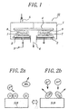
- Fig. 1 shows a known dry-etching equipment.
- a dry-etching equipment 10 has a chamber 1 and a RF electric power supply 3. Then, in the chamber 1, a susceptor 2 to hold a solid material 7, a plate 4, a gas inlet 5 and a gas outlet 6 are provided.
- the RF electric power source 3 is connected to the susceptor 2 and can generate an electric field having a given intensity with the plate 4 as an opposing electrode.
- an etching gas is introduced therein from the gas inlet 5.
- the etching gas pressure in the chamber 1 is maintained in a given value by controlling a gas introducing amount from the gas inlet 5 and an evacuation rate (a gas evacuating amount) from the gas outlet 6, and thereafter an etching gas plasma 8 is generated in between the susceptor 2 and the plate 4 by applying a given voltage from the RF electric power supply 3 to the susceptor 2 on which the solid material 7 is set.
- the following two step-dry etching enables the surfaces of the solid material to be dry-etched by one atomic layer or by one molecular layer:
- the above method has difficulty controlling the one atomic layer- or one molecular layer-dry etching in the case of dry-etching a solid material other than silicon or the like.
- the above method often has difficulty in dry-etching itself the solid material as well as the one molecular layer-dry etching or the like.
- Embodiments of the present invention aim to provide a dry-etching method and a dry-etching equipment usable for controlling one atomic layer order- or one molecular layer order-dry etching through the removing of the surfaces of the solid material composed of plural elements by one atomic layer or one molecular layer.
- the inventors have, in particular studied dry etching, through the controlling of one molecular layer dry etching, the solid material composed of the plural elements which itself has difficulty in being etched.
- the optimized vapor treatment condition during the dry-etching is different for each kind of the plural constituting elements. Then, it has also been found that by selecting each optimized vapor treatment condition for each kind of the plural constituting elements and thereby removing each kind of the constituting elements independently, the dry-etching of the solid material as above-mentioned can be carried out and the one molecular layer-dry etching can be realized.
- Figs. 2 show schematically an embodiment of the dry-etching process according to the present invention.
- Figs. 2 represent the dry-etching process in which a mixed gas of a hydrogen gas and an argon gas are employed for a solid material composed of silicon nitride.
- the flow rate ratio of the hydrogen gas and the argon gas in the mixed gas and the electric power to supply with the mixed gas are set to values suitable for the vapor treatment condition for nitrogen elements constituting the solid material and then, a given plasma is generated.
- excited hydrogen particles are reacted only with the nitrogen elements to generate etching induced substances having a NHx composition on the surfaces of the solid material, later removed from the surfaces.
- Figs. 4 show the XPS (X-ray photoelectron spectroscopy) intensity, from a surface of a silicon nitride film, of the silicon elements and the nitrogen elements constituting the silicon nitride film having a 12 ⁇ thickness when the silicon nitride film is dry-etched according to a method and equipment of the present invention.
- XPS intensities are represented as relative XPS intensities for silicon elements of a substrate as a standard.
- etching cycle means a repeated number of the cycle in which the nitrogen element-removal and the silicon element-removal are carried out, respectively.
- the one molecular layer-dry etching can be performed for the solid material, and thereby the solid material can be dry-etched in an extremely controlled manner.
- the dry-etching it enables the dry-etching to have a directionality, and thereby the solid material can be etched easily into a complex shape through the dry-etching. Moreover, high etching efficiency can be obtained.
- the incident energy is preferably 10-20eV, more preferably 13-17eV. It enables the etching ion particle to penetrate into the surface of the solid material by about one atomic layer or one molecular layer. Then, by removing the thus generated etching induced substances, the one atomic layer-or the one molecular layer-dry etching can be realized in good controllability.
- Fig. 3 is a schematic view showing a preferred embodiment in the dry-etching equipment according to the present invention.
- a dry-etching equipment 90 shown in Fig. 3 has a vacuum chamber 20, a turbo molecular pump 30, a susceptor 40 to set a solid material 45, a shutter 50 provided so as to cover the solid material 45, an ECR plasma-generating equipment 60, a gas flow rate-controlling equipment 70 and a sequence controller 80. Then, the turbo molecular pump 30 is connected to a valve 35 and through the opening and shutting of the valve, the interior of the vacuum chamber 20 is evacuated.
- the ECR plasma was introduced into the vacuum chamber 20 from the plasma inlet 68 and was irradiated to the silicon nitride film 45 by opening the shutter 50. At 45 minutes later, the shutter 50 was closed.
- a solid material having difficulty, being dry-etched can be treated by dry-etch.
- various kinds of solid material can be dry-etched through the controlling of one atomic layer or one molecular layer by selecting an appropriate vapor treatment condition for each kind of the constituting elements of the solid material.
Landscapes
- Physics & Mathematics (AREA)
- Engineering & Computer Science (AREA)
- Plasma & Fusion (AREA)
- Chemical & Material Sciences (AREA)
- Analytical Chemistry (AREA)
- Drying Of Semiconductors (AREA)
- ing And Chemical Polishing (AREA)
Abstract
Description
Claims (13)
- A method for dry-etching a solid material composed of plural constituting elements comprising steps of:setting the solid material on a supportvapor treating the solid material through the selection of a different vapor treatment condition for each of the constituting elements and thereby, removing each of the constituting elements independently.
- A dry-etching method as defined in claim 1, wherein the step of vapor-treating further comprises the steps of:plasma-exciting gas molecules in a vapor phase to generate etching particles, andintroducing the etching particles into the surfaces of the solid material and thereby removing the etching induced substances obtained from the reaction of the etching particles with the constituting elements of the solid material.
- A dry-etching method as defined in claim 2, wherein the incident energy of the etching particle to the surface of the solid material is not more than 25eV.
- A dry-etching method as defined in claim 3, wherein the incident energy of the etching particle to the surface of the solid material is 10-20eV.
- A dry-etching method as defined in any one of claim 1 to 4, wherein the different vapor treatment conditions are so determined that the gas molecular concentration may be different for each of the constituting elements.
- A dry-etching method as defined in any one of claims 1 to 5, wherein the different vapor treatment condition is so determined that the kind of gas molecule is different for each of the constituting elements.
- A dry-etching method as defined in any one of claims 2 to 6, wherein the different vapor treatment condition is so determined that the percentage of the plasma-excited particles may be different for each of the constituting elements.
- A dry-etching method as defined in any one of claims 2 to 7, wherein the solid material is composed of silicon nitride and the gas molecules are composed of hydrogen molecules.
- An equipment for dry-etching a solid material composed of plural constituting elements, wherein the solid material is dry-etched through the independent removing of each of the constituting elements by selecting the vapor treatment condition for each of the constituting elements.
- A dry-etching equipment as defined in claim 9, wherein the vapor treatment condition is a gas molecular concentration in a vapor phase.
- A dry-etching equipment as defined in claim 9 or 10, wherein the vapor treatment condition is a kind of gas molecule.
- A dry-etching equipment as defined in any one of claims 9 to 11, wherein the vapor treatment condition is a percentage of etching particles generated by plasma excitation.
- A dry-etching equipment comprising a vacuum chamber, a vacuum pump, a susceptor to set a solid material, a shutter provided so as to cover the solid material, an ECR plasma-generating equipment, a gas flow rate-controlling equipment and a sequence controller, the sequence controller controlling a gas flow rate and generation of an ECR plasma to provide a different vapor treatment condition for each of the constituting elements of the solid material, and then, opening or closing the shutter so as to synchronize the provision of the different vapor treatment conditions, whereby the solid material is dry-etched through the independent removing of each of the constituting elements.
Applications Claiming Priority (2)
| Application Number | Priority Date | Filing Date | Title |
|---|---|---|---|
| JP17367899A JP3378909B2 (en) | 1999-06-21 | 1999-06-21 | Dry etching method and apparatus |
| JP17367899 | 1999-06-21 |
Publications (2)
| Publication Number | Publication Date |
|---|---|
| EP1063691A2 true EP1063691A2 (en) | 2000-12-27 |
| EP1063691A3 EP1063691A3 (en) | 2002-08-21 |
Family
ID=15965081
Family Applications (1)
| Application Number | Title | Priority Date | Filing Date |
|---|---|---|---|
| EP00301655A Pending EP1063691A3 (en) | 1999-06-21 | 2000-03-01 | A dry-etching method and an equipment for dry-etching |
Country Status (2)
| Country | Link |
|---|---|
| EP (1) | EP1063691A3 (en) |
| JP (1) | JP3378909B2 (en) |
Cited By (1)
| Publication number | Priority date | Publication date | Assignee | Title |
|---|---|---|---|---|
| US6797637B2 (en) | 2002-05-14 | 2004-09-28 | Oki Electric Industry Co., Ltd. | Semiconductor device fabrication method |
Families Citing this family (1)
| Publication number | Priority date | Publication date | Assignee | Title |
|---|---|---|---|---|
| JP6983103B2 (en) * | 2018-04-23 | 2021-12-17 | 東京エレクトロン株式会社 | Processing equipment and embedding method |
Family Cites Families (6)
| Publication number | Priority date | Publication date | Assignee | Title |
|---|---|---|---|---|
| JPS6390133A (en) * | 1986-10-03 | 1988-04-21 | Toshiba Corp | Method for dry-etching silicon nitride film |
| JPH02272728A (en) * | 1989-04-14 | 1990-11-07 | Nec Corp | Dry etching method |
| JP2522050B2 (en) * | 1989-05-19 | 1996-08-07 | 日本電気株式会社 | Atomic layer dry etching method |
| US5385651A (en) * | 1991-01-11 | 1995-01-31 | University Of Georgia Research Foundation | Digital electrochemical etching of compound semiconductors |
| JPH04338640A (en) * | 1991-05-16 | 1992-11-25 | Nec Corp | Method and device for etching atomic layers |
| JPH0737807A (en) * | 1993-07-21 | 1995-02-07 | Hitachi Ltd | Surface treatment method using atomic and molecular beams and apparatus therefor |
-
1999
- 1999-06-21 JP JP17367899A patent/JP3378909B2/en not_active Expired - Lifetime
-
2000
- 2000-03-01 EP EP00301655A patent/EP1063691A3/en active Pending
Cited By (1)
| Publication number | Priority date | Publication date | Assignee | Title |
|---|---|---|---|---|
| US6797637B2 (en) | 2002-05-14 | 2004-09-28 | Oki Electric Industry Co., Ltd. | Semiconductor device fabrication method |
Also Published As
| Publication number | Publication date |
|---|---|
| JP3378909B2 (en) | 2003-02-17 |
| JP2001003185A (en) | 2001-01-09 |
| EP1063691A3 (en) | 2002-08-21 |
Similar Documents
| Publication | Publication Date | Title |
|---|---|---|
| US5368685A (en) | Dry etching apparatus and method | |
| US5376223A (en) | Plasma etch process | |
| US9659791B2 (en) | Metal removal with reduced surface roughness | |
| US6720260B1 (en) | Sequential electron induced chemical vapor deposition | |
| US9708707B2 (en) | Nanolayer deposition using bias power treatment | |
| US20040086434A1 (en) | Apparatus and method for treating objects with radicals generated from plasma | |
| KR100327950B1 (en) | Process for treating a substrate and apparatus for the same | |
| JPH05275392A (en) | Etching of sio2 film | |
| US5413954A (en) | Method of making a silicon-based device comprising surface plasma cleaning | |
| EP1035568A1 (en) | Method of plasma processing | |
| JP7116248B2 (en) | Plasma processing apparatus and plasma processing method | |
| JPH03263827A (en) | Digital etching apparatus | |
| JPH0380531A (en) | Method and apparatus for surface treating and thin film member | |
| US20250095983A1 (en) | Cyclic low temperature film growth processes | |
| JPH08124902A (en) | Plasma processing device | |
| JP3378909B2 (en) | Dry etching method and apparatus | |
| US20210246551A1 (en) | Systems for processing with mean free path limited species | |
| KR102353795B1 (en) | Monolayer-mediated precision material etching | |
| JPH04137532A (en) | Surface processing method and its equipment | |
| JP3408311B2 (en) | Digital etching method and apparatus | |
| US5194119A (en) | Method of anisotropic dry etching of thin film semiconductors | |
| JPH07263421A (en) | Surface treatment method and surface treatment apparatus | |
| JP7634106B2 (en) | Etching Method | |
| US20250125124A1 (en) | Electron beam-induced and remote plasma-assisted simultaneous material-selective etching and growth | |
| WO2020186087A1 (en) | Selective silicon dioxide removal using low pressure low bias deuterium plasma |
Legal Events
| Date | Code | Title | Description |
|---|---|---|---|
| PUAI | Public reference made under article 153(3) epc to a published international application that has entered the european phase |
Free format text: ORIGINAL CODE: 0009012 |
|
| 17P | Request for examination filed |
Effective date: 20000502 |
|
| AK | Designated contracting states |
Kind code of ref document: A2 Designated state(s): AT BE CH CY DE DK ES FI FR GB GR IE IT LI LU MC NL PT SE |
|
| AX | Request for extension of the european patent |
Free format text: AL;LT;LV;MK;RO;SI |
|
| PUAL | Search report despatched |
Free format text: ORIGINAL CODE: 0009013 |
|
| STAA | Information on the status of an ep patent application or granted ep patent |
Free format text: STATUS: THE APPLICATION HAS BEEN WITHDRAWN |
|
| 18W | Application withdrawn |
Withdrawal date: 20020612 |
|
| D18W | Application withdrawn (deleted) | ||
| AK | Designated contracting states |
Kind code of ref document: A3 Designated state(s): AT BE CH CY DE DK ES FI FR GB GR IE IT LI LU MC NL PT SE |
|
| AX | Request for extension of the european patent |
Free format text: AL;LT;LV;MK;RO;SI |
|
| R18W | Application withdrawn (corrected) |
Effective date: 20020612 |