EP1063670A2 - Bonded article with improved work function uniformity and method for making the same - Google Patents
Bonded article with improved work function uniformity and method for making the same Download PDFInfo
- Publication number
- EP1063670A2 EP1063670A2 EP00305016A EP00305016A EP1063670A2 EP 1063670 A2 EP1063670 A2 EP 1063670A2 EP 00305016 A EP00305016 A EP 00305016A EP 00305016 A EP00305016 A EP 00305016A EP 1063670 A2 EP1063670 A2 EP 1063670A2
- Authority
- EP
- European Patent Office
- Prior art keywords
- single crystal
- cathode
- crystal cathode
- tantalum
- bonded article
- Prior art date
- Legal status (The legal status is an assumption and is not a legal conclusion. Google has not performed a legal analysis and makes no representation as to the accuracy of the status listed.)
- Granted
Links
Images




Classifications
-
- H—ELECTRICITY
- H01—ELECTRIC ELEMENTS
- H01J—ELECTRIC DISCHARGE TUBES OR DISCHARGE LAMPS
- H01J1/00—Details of electrodes, of magnetic control means, of screens, or of the mounting or spacing thereof, common to two or more basic types of discharge tubes or lamps
- H01J1/02—Main electrodes
- H01J1/13—Solid thermionic cathodes
- H01J1/15—Cathodes heated directly by an electric current
-
- H—ELECTRICITY
- H10—SEMICONDUCTOR DEVICES; ELECTRIC SOLID-STATE DEVICES NOT OTHERWISE PROVIDED FOR
- H10P—GENERIC PROCESSES OR APPARATUS FOR THE MANUFACTURE OR TREATMENT OF DEVICES COVERED BY CLASS H10
- H10P76/00—Manufacture or treatment of masks on semiconductor bodies, e.g. by lithography or photolithography
-
- H—ELECTRICITY
- H01—ELECTRIC ELEMENTS
- H01J—ELECTRIC DISCHARGE TUBES OR DISCHARGE LAMPS
- H01J37/00—Discharge tubes with provision for introducing objects or material to be exposed to the discharge, e.g. for the purpose of examination or processing thereof
- H01J37/02—Details
- H01J37/04—Arrangements of electrodes and associated parts for generating or controlling the discharge, e.g. electron-optical arrangement or ion-optical arrangement
- H01J37/06—Electron sources; Electron guns
-
- H—ELECTRICITY
- H01—ELECTRIC ELEMENTS
- H01J—ELECTRIC DISCHARGE TUBES OR DISCHARGE LAMPS
- H01J9/00—Apparatus or processes specially adapted for the manufacture, installation, removal, maintenance of electric discharge tubes, discharge lamps, or parts thereof; Recovery of material from discharge tubes or lamps
- H01J9/02—Manufacture of electrodes or electrode systems
- H01J9/04—Manufacture of electrodes or electrode systems of thermionic cathodes
-
- H—ELECTRICITY
- H01—ELECTRIC ELEMENTS
- H01J—ELECTRIC DISCHARGE TUBES OR DISCHARGE LAMPS
- H01J2237/00—Discharge tubes exposing object to beam, e.g. for analysis treatment, etching, imaging
- H01J2237/30—Electron or ion beam tubes for processing objects
- H01J2237/317—Processing objects on a microscale
- H01J2237/3175—Lithography
Definitions
- the present invention relates to a bonded article for use in electron beam projection lithography and a method for making the bonded article, and more particularly, to a bonded article including a cathode with an improved work function and a method for making the bonded article including the improved work function cathode utilizing a localized bonding technique.
- Projection electron beam lithography such as Scattering Angular Limitation Projection Electron Beam Lithograph (SCALPELTM)
- SCALPELTM Scattering Angular Limitation Projection Electron Beam Lithograph
- the SCALPELTM mask has a membrane of a low atomic number material on which is formed a layer of high atomic number material.
- the layer of high atomic number material has a pattern delineated therein.
- Both the low atomic number membrane material and the high atomic number patterned layer of material are transparent to the electrons projected thereon (i.e., electrons with an energy of about 100 keV).
- the low atomic number membrane materials scatters the electrons weakly and at small angles.
- the high atomic number patterned layer of material scatters the electrons strongly and at large angles.
- the electrons transmitted through the high atomic number patterned material have a larger scattering angle than the electrons transmitted through the membrane. This difference in scattering angle provides a contrast between the electrons transmitted through the membrane alone and the electrons transmitted through the layer of patterned material formed on the membrane.
- the back focal pane filter has an aperture therein.
- the weakly scattered electrons are transmitted through the aperture while the strongly scattered electrons are blocked by the back focal plane filter.
- the image of the pattern defined in the weakly scattered electrons is transmitted through the aperture and into the layer of energy sensitive material.
- FIG. 1 is a schematic diagram illustrating the concept of a conventional SCALPELTM system.
- a beam B of electrons 10 is directed towards a scattering mask 9 including a thin membrane 11 having a thickness between about 1,000 ⁇ and about 20,000 ⁇ (0.1 ⁇ m and about 2 ⁇ m thick).
- the membrane 11 is composed of a material which is virtually transparent to the electron beam B composed of electrons 10. That is to say that electrons 10 in beam B pass through membrane 11 freely in the absence of any other object providing an obstruction to the path of electrons 10 in the beam B as they pass from the source of the beam through the membrane 11.
- a pattern of high density scattering elements 12 Formed on the side of the membrane 11 facing the beam 10, is a pattern of high density scattering elements 12 to provide a contrast mechanism that enables reproduction of the mask pattern at the target surface.
- the scattering elements 12 are patterned in the composite shape which is to be exposed upon a work piece 17 (usually a silicon wafer) which is coated with E-beam sensitive resist, which as shown in FIG. 1 has been processed into pattern elements 18.
- the electrons 10 from the E-beam B which pass through the mask 9 are shown by beams 14 which pass through electromagnetic lens 15 which focuses the beams 14 through an aperture 16' into an otherwise opaque back focal plane filter 16.
- the aperture 16' permits only electrons scattered at small angles to pass through to the work piece 17.
- the exposure tool 20 includes a source 22 (usually an electron gun), a mask stage 24, imaging optics 26, and a wafer stage 28.
- the mask stage 24 and the wafer stage 28 are mounted to the top and bottom of a block of aluminum, referred to as the metrology plate 30.
- the metrology plate 30, which is on the order of 3000 lbs., serves as a thermal and mechanical stabilizer for the entire exposure tool 20.
- FIG. 3 illustrates a prior art source 22 in more detail.
- the source 22 includes a cathode 42, an anode 43, a grid electrode 44, focusing plates 45, and a filament 46.
- the cathode 42 and the filament 46 comprise a conventional bonded article 49.
- Each of the cathode 42, anode 43, grid electrode 44, and focusing plates 45 exhibit substantial circular and radial symmetry about an imaginary line of focus 50.
- the cathode 42 is made of gallium arsenide (GaAs), bialkali cathode materials, cesium antimonide (Cs 3 Sb), or a pure material having a low work function, such as tantalum (Ta), samarium (Sm), or nickel (Ni).
- the cathode 42 is made of a metal added to a semiconductor material by mixing or by depositing through sputtering or annealing.
- the metal is preferably tantalum (Ta), copper (Cu), silver (Ag), aluminum (Al), or gold (Au), or oxides or halides of these metals.
- One such example of a prior art cathode is constructed from tantalum (Ta) annealed on the surface of nickel (Ni).
- thermionic cathodes such as pure metal (tungsten or tantalum), lanthanum hexaboride (LaB 6 ), etc. cathodes are sufficient for these applications.
- thermoionic cathodes have work function variations substantially greater than 2%, for example 5-10%.
- the SCALPELTM process requires a thermoionic cathode with a work function variation less than 2%
- the conventional thermoionic cathodes which meet the SCALPELTM requirements for other parameters, such as emission uniformity, low work function, low evaporation rate, high voltage operating environment, and vacuum contamination resilience are tantalum (Ta) cathodes (such as the cathode disclosed in U.S. Patent No. 5,426,686) having a disk shape.
- the disk-shaped tantalum (Ta) cathode is made from cold or hot rolled tantalum (Ta) foils which are hot pressed into a micro-polycrystalline material. Because of its polycrystalline nature, the grains are misoriented with each other on the order of 5-20°.
- the conventional polycrystalline Ta cathode also has an uncontrolled grain size distribution between 5-400 ⁇ m.
- the conventional polycrystalline Ta cathode work function distribution is "patchy", varying from grain-to-grain (because of differing orientations and sizes) and resulting in an unacceptably patchy or nonuniform emission pattern. Growth of the misoriented and differing sized grains further aggravates the patchiness problem. The non-uniformities caused by grain misorientation, grain size differences, and grain growth on the cathode surface are transferred by the SCALPELTM electron optics down to the shaping aperture (the object plane) and eventually to the wafer surface (the imaging plane).
- the conventional polycrystalline cathode materials When used as a SCALPELTM cathode, the conventional polycrystalline cathode materials experience grain growth and rough texture development at the SCALPELTM high operating temperatures (1200-2000°C) and extended time period (greater than 1000 hours). Although the total emission current is satisfactory, structural developments at the cathode surface causes dark spots to appear on the cathode surface and make the cathode unacceptable for SCALPELTM. In addition, conventional cathode materials, such as LaB 6 , are easily contaminated by the SCALPELTM operating environment, as described in "Design of a low-brightness, highly uniform source for projection electron-beam lithography (SCALPEL)", W.K. Waskiewicz et al., Proc. SPIE, 3155 (1997).
- SCALPEL design of a low-brightness, highly uniform source for projection electron-beam lithography
- cathodes such as cathode 42 illustrated in Figure 3 and cathodes made of LaB 6 are bonded to their corresponding filament 46 by traditional global bonding techniques, such as spot welding.
- spot welding modifies the structure of a large area adjacent to the weld spot.
- the filament 46 in order to bond the filament 46 and the cathode 42, the filament 46 must be pressed heavily against the surface of the cathode 42 and a high current must be run through to bring the point of interaction to a very high temperature.
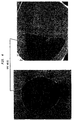
- Figure 4 illustrates two examples of a misoriented crystalline center induced by spot welding.
- the present invention solves the problems with conventional bonded articles used in SCALPELTM and similar projection electron lithography systems by providing a bonded article including a single crystal cathode and a member that provides heat and/or structural support, where the crystal structure of the single crystal cathode is preserved after bonding to the member.
- the single crystal cathode of the present invention need not be an absolute "single" crystal, but is defined as a structure that has ⁇ 1° variations. Because of its single crystalline structure, the single crystal cathode does not have misoriented grains. As a result, the single crystal cathode of the present invention has fewer structural non-uniformities than the conventional micro-polycrystalline foils and therefore, a more uniform emission characteristic.
- the single crystal cathode is made of tantalum.
- the present invention also solves the problems with bonding a single crystal cathode of the present invention with conventional heat supplying and/or structural support members (such as filament 46 in Figure 3) used in SCALPELTM and similar projection electron lithography systems by utilizing a local bonding technique to bond the single crystal cathode and the member together.
- a local bonding technique does not recrystallize a center of the single crystal cathode, and therefore produces a bonded single crystal cathode and member which is usable in a projection electron lithography system, such as the SCALPELTM system.
- the local bonding technique is laser welding.
- the member is a filament that provides both heat and structural support to the single crystal cathode.
- the single crystal cathode is made of tantalum and the filament is made of one of tungsten, a tungsten-rhenium alloy, and a tungsten-tantalum alloy.
- FIG. 5 illustrates a general cathode 110 of the present invention in one embodiment.
- cathode 110 is a single crystal, in contrast to the conventional micro-polycrystalline tantalum foils.
- the single crystal cathode of the present invention need not be an absolute "single" crystal, but is defined as a structure that has ⁇ 1° variations. Because of its single crystalline structure, the single crystal cathode does not have misoriented grains. As a result, the cathode 110 of the present invention has fewer structural non-uniformities than the conventional micro-polycrystalline foils and therefore, a more uniform emission characteristic. As a result, the single crystal cathode 110 of the present invention solves the patchiness problems with conventional cathodes. Further, one or more of the crystalline planes of the single crystal cathode 110 has a work function variation substantially less than 2%, which is sufficiently uniform to be used as SCALPELTM (and similar projection electron lithography) process thermoionic cathode.
- the cathode 110 is made of a refractory crystalline material, such as tantalum, tungsten, rhenium or molybdenum. In another preferred embodiment, the cathode 110 is made of an alloy including at least one of tantalum, tungsten, rhenium or molybdenum.
- the single crystal cathode 110 is made of tantalum. Tantalum has a body centered cubic (bcc) structure. As illustrated in Figure 5, both emissive planes A (100) and B (111) of the tantalum single crystal have relatively low work functions, 4.0 eV and 4.15 eV, respectively, in contrast to conventional polycrystalline foil cathodes, which have work functions of approximately 4.25 eV. Emissive plane C (110) has a relatively high work function of 4.8 eV. As is known to one of ordinary skill in the art, work function and current are inversely related; the lower the work function, the higher the current that can be generated. Therefore, both emissive planes A (100) and B (111) permit the SCALPELTM system in which they are used, to produce a higher current.
- bcc body centered cubic
- Figure 6 illustrates a method of bonding the general cathode 110 to a conventional heat supplying/structural member, such as filament 46 in Figure 3, to produce a bonded article, in one embodiment of the present invention.
- steps 200 and 210 the single crystal cathode 110 and filament 46, respectively, are obtained.
- step 220 the single crystal cathode 110 and filament 46 are bonded using a local bonding technique.
- a global bonding technique such as spot welding cannot be used to bond the cathode 110 of the present invention to a filament 46, because spot welding modifies the structure of the single crystal cathode 110 in an area adjacent to the weld spot.
- the filament 46 must be pressed heavily against a surface of the tantalum single crystal and a high current (up to 1,000 A) must be run through to bring the point of interaction to a temperature of at least 3,000°C.
- the high current runs through the entire cathode 110 causing global thermal radiance and related stress/tension over the entire cathode 110.
- the present invention solves the problems with bonding a single crystal cathode of the present invention with conventional filaments by utilizing a local bonding technique to bond the single crystal cathode 110 and the filament 46 together.
- a local bonding technique does not recrystallize (by causing the grain misorientation to increase to 5-20°) a center of the single crystal cathode, and therefore produces a bonded article including single crystal cathode 110 and filament 46 which is usable in a projection electron lithography system, such as the SCALPELTM system.
- the local bonding technique is laser welding.
- Laser welding is significantly different from traditional spot welding, in that laser welding does not depend on sample surface roughness, surface and volumetric electrical resistance, supporting jig resistance, sample and jig thermal conductivity. Laser welding does depend on the sample melting point and to some extent, on the sample surface optical reflection and cleanness. As a result, laser welding is effective in bonding two different materials, for example molybdenum and stainless steel or iridium and tungsten. Another attractive feature of laser welding is its inherent "pointness"; the laser spot is tightly focused down to a 150-200 ⁇ m Dia. and the weld depth does not even approach 50 ⁇ m.
- laser welding can be thermally characterized as a pure adiabatic process, namely, when a cathode's microscopic area is melted, the surrounding area remains cold.
- This is one major advantage of laser welding over spot welding namely, laser welding works on microscopic part of an entire cathode, whereas spot welding affects a large cathode area.
- the single crystal cathode is made of tantalum. In an even more preferred embodiment, the single crystal cathode is disk-shaped and has a diameter of 600-1500 ⁇ m and a height of 200-300 ⁇ m. In an even more preferred embodiment, the conventional member is both a heat supplying and structural support member. In an even more preferred embodiment, the conventional member is a ribbon shaped filament. In an even more preferred embodiment, the filament is made of one of tungsten, a tungsten-rhenium alloy, and a tungsten-tantalum alloy. In an even more preferred embodiment, the single crystal cathode 110 is utilized in a source which includes KovarTM or molybdenum/rhenium (Mo/Re) posts, and a tungsten (W) filament.
- Mo/Re molybdenum/rhenium
- a typical tantalum single crystal cathode disc dimensions are 1mm Dia and 0.2 mm thickness, and its mass is 2.6 x 10 -3 gms.
- the specific heat of tantalum is 0.15 J/gm. If a laser weld spot is 200 ⁇ Dia and 50 ⁇ deep, the tantalum mass to be melted is 2.7 x 10 -5 g, and assuming the necessary spot temperature elevation from room temperature to a melting point of 3,000°C, the amount of absorbed heat is 12 mJ. If this heat is dissipated entirely in the tantalum cathode, then the entire tantalum cathode disc would be warmed only by 62°C.
- FIG. 7 illustrates a laser-welded tantalum single crystalline cathode emission image. As illustrated in Figure 7, neither grains nor boundaries are detected. As desired, the laser weld did not adversely affect the cathode's sensitive crystalline structure.
Landscapes
- Engineering & Computer Science (AREA)
- Manufacturing & Machinery (AREA)
- Chemical & Material Sciences (AREA)
- Analytical Chemistry (AREA)
- Electron Beam Exposure (AREA)
- Electron Sources, Ion Sources (AREA)
- Solid Thermionic Cathode (AREA)
- Crystals, And After-Treatments Of Crystals (AREA)
Abstract
Description
Claims (20)
- A bonded article comprising:a single crystal cathode; anda member, bonded to said substantially single crystal cathode such that a single crystalline structure of the single crystal cathode is preserved after bonding.
- The bonded article of claim 1, said single crystal cathode having reduced structural and emissive non-uniformities.
- The bonded article of claim 1, wherein said single crystal cathode is made of tantalum.
- The bonded article of claim 3, wherein an emissive plane of said substantially single crystal cathode has a relatively low work function.
- The bonded article of claim 4, wherein the emissive plane is the (111) plane.
- The bonded article of claim 4, wherein the emissive plane is the (100) plane.
- The bonded article of claim 1, wherein said single crystal cathode is a refractory crystalline material or alloy with a relatively low work function.
- The bonded article of claim 1, wherein said single crystal cathode is part of a projection electron lithography system.
- The bonded article of claim 8, wherein the projection electron lithography system is a SCALPEL™ system.
- A method of bonding a single crystal cathode, having a grain structure, to a member, comprising:obtaining the single crystal cathode;obtaining the member; andbonding the single crystal cathode and the member together by a local bonding technique, such that a single crystalline structure of the single crystal cathode is preserved after bonding.
- The method claim 10, wherein the local bonding technique is laser welding.
- The method of claim 10, wherein the single crystal cathode has reduced structural and emissive non-uniformities.
- The method of claim 10, wherein the single crystal cathode is made of tantalum.
- The method of claim 13, wherein an emissive plane of said single crystal cathode has a relatively low work function.
- The method of claim 14, wherein the emissive plane is the (111) plane.
- The method of claim 14, wherein the emissive plane is the (100) plane.
- The method of claim 10, wherein the single crystal cathode is a refractory crystalline material or alloy with a relatively low work function.
- The method of claim 10 , wherein the single crystal cathode is part of a projection electron lithography system.
- The method of claim 18 , wherein the projection electron lithography system is a SCALPEL™ system.
- The method of claim 10, wherein the member is a filament, made of one of tungsten, a tungsten-rhenium alloy, and a tungsten-tantalum alloy.
Applications Claiming Priority (2)
| Application Number | Priority Date | Filing Date | Title |
|---|---|---|---|
| US337741 | 1994-11-14 | ||
| US09/337,741 US6448569B1 (en) | 1999-06-22 | 1999-06-22 | Bonded article having improved crystalline structure and work function uniformity and method for making the same |
Publications (3)
| Publication Number | Publication Date |
|---|---|
| EP1063670A2 true EP1063670A2 (en) | 2000-12-27 |
| EP1063670A3 EP1063670A3 (en) | 2006-05-10 |
| EP1063670B1 EP1063670B1 (en) | 2009-11-25 |
Family
ID=23321794
Family Applications (1)
| Application Number | Title | Priority Date | Filing Date |
|---|---|---|---|
| EP00305016A Expired - Lifetime EP1063670B1 (en) | 1999-06-22 | 2000-06-13 | Bonded article with improved work function uniformity and method for making the same |
Country Status (6)
| Country | Link |
|---|---|
| US (1) | US6448569B1 (en) |
| EP (1) | EP1063670B1 (en) |
| JP (2) | JP2001052594A (en) |
| KR (1) | KR20010049594A (en) |
| DE (1) | DE60043373D1 (en) |
| TW (1) | TW432396B (en) |
Cited By (1)
| Publication number | Priority date | Publication date | Assignee | Title |
|---|---|---|---|---|
| GB2583359A (en) * | 2019-04-25 | 2020-10-28 | Aquasium Tech Limited | Electron beam emitting assembly |
Families Citing this family (3)
| Publication number | Priority date | Publication date | Assignee | Title |
|---|---|---|---|---|
| US9138913B2 (en) * | 2005-09-08 | 2015-09-22 | Imra America, Inc. | Transparent material processing with an ultrashort pulse laser |
| EP2553711B1 (en) * | 2010-04-02 | 2015-09-02 | Koninklijke Philips N.V. | Ceramic metal halide lamp with feedthrough comprising an iridium wire |
| SG10201903641TA (en) * | 2014-10-23 | 2019-05-30 | Agency Science Tech & Res | Method of bonding a first substrate and a second substrate |
Family Cites Families (12)
| Publication number | Priority date | Publication date | Assignee | Title |
|---|---|---|---|---|
| GB395439A (en) * | 1932-02-17 | 1933-07-20 | Mullard Radio Valve Co Ltd | Improvements relating to thermionic valves |
| US2410822A (en) * | 1942-01-03 | 1946-11-12 | Sperry Gyroscope Co Inc | High frequency electron discharge apparatus |
| US2892740A (en) * | 1957-01-08 | 1959-06-30 | Univ Notre Dame Du Lac | Thermionic emitter and method of making same |
| US3284657A (en) * | 1963-06-03 | 1966-11-08 | Varian Associates | Grain-oriented thermionic emitter for electron discharge devices |
| NL7003279A (en) * | 1970-03-07 | 1971-09-09 | ||
| US4055780A (en) * | 1975-04-10 | 1977-10-25 | National Institute For Researches In Inorganic Materials | Thermionic emission cathode having a tip of a single crystal of lanthanum hexaboride |
| JPS5679828A (en) * | 1979-12-05 | 1981-06-30 | Toshiba Corp | Electron gun |
| CH672860A5 (en) * | 1986-09-29 | 1989-12-29 | Balzers Hochvakuum | |
| US5042058A (en) | 1989-03-22 | 1991-08-20 | University Of California | Ultrashort time-resolved x-ray source |
| JP3397570B2 (en) * | 1996-04-02 | 2003-04-14 | 電気化学工業株式会社 | Thermal field emission cathode |
| TW357380B (en) * | 1996-05-21 | 1999-05-01 | Toshiba Co Ltd | Manufacturing method of cathode structure, electronic gun structure, electronic tube, heater and cathode structures |
| JPH1131469A (en) * | 1997-07-08 | 1999-02-02 | Nikon Corp | Electron gun |
-
1999
- 1999-06-22 US US09/337,741 patent/US6448569B1/en not_active Expired - Lifetime
-
2000
- 2000-06-13 DE DE60043373T patent/DE60043373D1/en not_active Expired - Lifetime
- 2000-06-13 EP EP00305016A patent/EP1063670B1/en not_active Expired - Lifetime
- 2000-06-21 JP JP2000186628A patent/JP2001052594A/en active Pending
- 2000-06-22 TW TW089112268A patent/TW432396B/en not_active IP Right Cessation
- 2000-06-22 KR KR1020000034430A patent/KR20010049594A/en not_active Ceased
-
2007
- 2007-05-16 JP JP2007130041A patent/JP5392995B2/en not_active Expired - Fee Related
Cited By (3)
| Publication number | Priority date | Publication date | Assignee | Title |
|---|---|---|---|---|
| GB2583359A (en) * | 2019-04-25 | 2020-10-28 | Aquasium Tech Limited | Electron beam emitting assembly |
| WO2020217062A1 (en) * | 2019-04-25 | 2020-10-29 | Aquasium Technology Limited | Electron beam emitting assembly |
| JP2022530418A (en) * | 2019-04-25 | 2022-06-29 | アクアジウム・テクノロジー・リミテッド | Electron beam radiation assembly |
Also Published As
| Publication number | Publication date |
|---|---|
| TW432396B (en) | 2001-05-01 |
| US6448569B1 (en) | 2002-09-10 |
| EP1063670A3 (en) | 2006-05-10 |
| DE60043373D1 (en) | 2010-01-07 |
| JP2001052594A (en) | 2001-02-23 |
| EP1063670B1 (en) | 2009-11-25 |
| JP2007250554A (en) | 2007-09-27 |
| KR20010049594A (en) | 2001-06-15 |
| JP5392995B2 (en) | 2014-01-22 |
Similar Documents
| Publication | Publication Date | Title |
|---|---|---|
| EP0447832B1 (en) | X-ray tube target | |
| JP7117452B2 (en) | High brightness reflection type X-ray source | |
| JPS6255931A (en) | Formation of metal silicide contact and sputtering apparatustherefor | |
| TWI829864B (en) | Photocathode emitters and methods for operating the same | |
| EP1063670B1 (en) | Bonded article with improved work function uniformity and method for making the same | |
| US4799250A (en) | Rotating anode with graphite for X-ray tube | |
| US20040012338A1 (en) | Emitter with dielectric layer having implanted conducting centers | |
| JPH02291643A (en) | Electron gun with integral shadow grid | |
| US6162566A (en) | Mask holder for supporting transfer mask | |
| EP2188826B1 (en) | X-ray tube with enhanced small spot cathode and methods for manufacture thereof | |
| JP2003529183A (en) | Photocathode for electron source supported by diamond | |
| JP2002298772A (en) | Transmission radiation type X-ray tube and method of manufacturing the same | |
| KR20030036013A (en) | Tunneling emitters and method of making | |
| JPS6223418B2 (en) | ||
| EP1063669B1 (en) | Cathode with improved work function and method for making the same | |
| EP0392615B1 (en) | Colour display tube and display device comprising such a colour display tube | |
| US20100108641A1 (en) | Lavacoat pre-clean and pre-heat | |
| US20250140507A1 (en) | Method for producing an anode for a cold cathode x-ray source | |
| JPH09232209A (en) | Aperture mask for charged particle beam exposure apparatus and method of manufacturing the same | |
| Katsap et al. | Uniform large-area thermionic cathode for SCALPEL | |
| JPH08236049A (en) | X-ray tube | |
| JPH11297189A (en) | Field emission cold cathode and method of manufacturing the same | |
| JPS59108233A (en) | Impregnated cathode structure | |
| KR20010104552A (en) | Structure and Manufacturing Method of the Cathode with Impregnated type for Cathode Ray tube | |
| JPH11213856A (en) | Method for producing impregnated cathode structure and cathode substrate |
Legal Events
| Date | Code | Title | Description |
|---|---|---|---|
| PUAI | Public reference made under article 153(3) epc to a published international application that has entered the european phase |
Free format text: ORIGINAL CODE: 0009012 |
|
| AK | Designated contracting states |
Kind code of ref document: A2 Designated state(s): AT BE CH CY DE DK ES FI FR GB GR IE IT LI LU MC NL PT SE |
|
| AX | Request for extension of the european patent |
Free format text: AL;LT;LV;MK;RO;SI |
|
| PUAL | Search report despatched |
Free format text: ORIGINAL CODE: 0009013 |
|
| AK | Designated contracting states |
Kind code of ref document: A3 Designated state(s): AT BE CH CY DE DK ES FI FR GB GR IE IT LI LU MC NL PT SE |
|
| AX | Request for extension of the european patent |
Extension state: AL LT LV MK RO SI |
|
| 17P | Request for examination filed |
Effective date: 20060712 |
|
| 17Q | First examination report despatched |
Effective date: 20060913 |
|
| AKX | Designation fees paid |
Designated state(s): DE FR GB |
|
| 17Q | First examination report despatched |
Effective date: 20060913 |
|
| GRAP | Despatch of communication of intention to grant a patent |
Free format text: ORIGINAL CODE: EPIDOSNIGR1 |
|
| GRAC | Information related to communication of intention to grant a patent modified |
Free format text: ORIGINAL CODE: EPIDOSCIGR1 |
|
| RAP3 | Party data changed (applicant data changed or rights of an application transferred) |
Owner name: LUCENT TECHNOLOGIES INC. |
|
| GRAS | Grant fee paid |
Free format text: ORIGINAL CODE: EPIDOSNIGR3 |
|
| GRAA | (expected) grant |
Free format text: ORIGINAL CODE: 0009210 |
|
| AK | Designated contracting states |
Kind code of ref document: B1 Designated state(s): DE FR GB |
|
| REG | Reference to a national code |
Ref country code: GB Ref legal event code: FG4D |
|
| REF | Corresponds to: |
Ref document number: 60043373 Country of ref document: DE Date of ref document: 20100107 Kind code of ref document: P |
|
| PLBE | No opposition filed within time limit |
Free format text: ORIGINAL CODE: 0009261 |
|
| STAA | Information on the status of an ep patent application or granted ep patent |
Free format text: STATUS: NO OPPOSITION FILED WITHIN TIME LIMIT |
|
| 26N | No opposition filed |
Effective date: 20100826 |
|
| PGFP | Annual fee paid to national office [announced via postgrant information from national office to epo] |
Ref country code: FR Payment date: 20140609 Year of fee payment: 15 |
|
| PGFP | Annual fee paid to national office [announced via postgrant information from national office to epo] |
Ref country code: GB Payment date: 20150527 Year of fee payment: 16 |
|
| REG | Reference to a national code |
Ref country code: FR Ref legal event code: ST Effective date: 20160229 |
|
| PG25 | Lapsed in a contracting state [announced via postgrant information from national office to epo] |
Ref country code: FR Free format text: LAPSE BECAUSE OF NON-PAYMENT OF DUE FEES Effective date: 20150630 |
|
| PGFP | Annual fee paid to national office [announced via postgrant information from national office to epo] |
Ref country code: DE Payment date: 20160524 Year of fee payment: 17 |
|
| GBPC | Gb: european patent ceased through non-payment of renewal fee |
Effective date: 20160613 |
|
| PG25 | Lapsed in a contracting state [announced via postgrant information from national office to epo] |
Ref country code: GB Free format text: LAPSE BECAUSE OF NON-PAYMENT OF DUE FEES Effective date: 20160613 |
|
| REG | Reference to a national code |
Ref country code: DE Ref legal event code: R119 Ref document number: 60043373 Country of ref document: DE |
|
| PG25 | Lapsed in a contracting state [announced via postgrant information from national office to epo] |
Ref country code: DE Free format text: LAPSE BECAUSE OF NON-PAYMENT OF DUE FEES Effective date: 20180103 |
|
| REG | Reference to a national code |
Ref country code: DE Ref legal event code: R082 Ref document number: 60043373 Country of ref document: DE Representative=s name: DILG HAEUSLER SCHINDELMANN PATENTANWALTSGESELL, DE Ref country code: DE Ref legal event code: R081 Ref document number: 60043373 Country of ref document: DE Owner name: AVAGO TECHNOLOGIES GENERAL IP (SINGAPORE) PTE., SG Free format text: FORMER OWNER: LUCENT TECHNOLOGIES, INC., MURRAY HILL, N.J., US |