EP1063596A2 - Circuit and method for reliably performing bus reset regardless of cable length - Google Patents
Circuit and method for reliably performing bus reset regardless of cable length Download PDFInfo
- Publication number
- EP1063596A2 EP1063596A2 EP00113025A EP00113025A EP1063596A2 EP 1063596 A2 EP1063596 A2 EP 1063596A2 EP 00113025 A EP00113025 A EP 00113025A EP 00113025 A EP00113025 A EP 00113025A EP 1063596 A2 EP1063596 A2 EP 1063596A2
- Authority
- EP
- European Patent Office
- Prior art keywords
- signal
- response
- state
- selector
- bus reset
- Prior art date
- Legal status (The legal status is an assumption and is not a legal conclusion. Google has not performed a legal analysis and makes no representation as to the accuracy of the status listed.)
- Withdrawn
Links
Images



Classifications
-
- G—PHYSICS
- G06—COMPUTING OR CALCULATING; COUNTING
- G06F—ELECTRIC DIGITAL DATA PROCESSING
- G06F13/00—Interconnection of, or transfer of information or other signals between, memories, input/output devices or central processing units
- G06F13/38—Information transfer, e.g. on bus
- G06F13/42—Bus transfer protocol, e.g. handshake; Synchronisation
- G06F13/4247—Bus transfer protocol, e.g. handshake; Synchronisation on a daisy chain bus
- G06F13/426—Bus transfer protocol, e.g. handshake; Synchronisation on a daisy chain bus using an embedded synchronisation, e.g. Firewire bus, Fibre Channel bus, SSA bus
-
- H—ELECTRICITY
- H04—ELECTRIC COMMUNICATION TECHNIQUE
- H04L—TRANSMISSION OF DIGITAL INFORMATION, e.g. TELEGRAPHIC COMMUNICATION
- H04L12/00—Data switching networks
- H04L12/28—Data switching networks characterised by path configuration, e.g. LAN [Local Area Networks] or WAN [Wide Area Networks]
- H04L12/40—Bus networks
-
- G—PHYSICS
- G06—COMPUTING OR CALCULATING; COUNTING
- G06F—ELECTRIC DIGITAL DATA PROCESSING
- G06F2213/00—Indexing scheme relating to interconnection of, or transfer of information or other signals between, memories, input/output devices or central processing units
- G06F2213/0012—High speed serial bus, e.g. IEEE P1394
Definitions
- the present invention relates to transmission and reception of signals between devices (nodes) attached to a computer over a serial bus such as the IEEE-1394 bus specified according to the IEEE-1394 Standard for a High Performance Serial Bus (or IEEE Std 1394-1995).
- a serial bus such as the IEEE-1394 bus specified according to the IEEE-1394 Standard for a High Performance Serial Bus (or IEEE Std 1394-1995).
- the IEEE 1394 standard specifies protocols for the transmission and reception of various control signals and communication signals between peripheral devices of a computer such as printers, hard disk drives, scanners, digital cameras (nodes) at different layers of each node connected to a serial bus.
- a procedure is specified for bus initialisation and determination of bus ownership. This procedure is described by a state machine having four broadly classified functions.
- the bus initialisation procedure consists of three network initialisation processes (Bus Reset process, Tree ID process, and Self ID process) and a Normal process (for normal communication between nodes).
- states R0 (Reset Start) and R1 (Reset Wait) are defined
- Tree ID process states T0 (Tree ID start), T1 (Child Handshake), T2 (Parent Handshake) and T3 (Root Contention) are defined.
- five states are defined for Self ID process, including S0 (Self ID Start), S1 (Self ID Grant), S2 (Self ID) Receive), S3 (Send Speed Capabilities) and S4 (Self ID Transmit)
- six states are defined for Normal process, including A0 (Idle), A1 (Request), A2 (Grant), TX (Transmit), RX (Receive) and PH (PHY Response).
- the present invention is primarily concerned with the operation of the Bus Reset process.
- Two bus reset processes are defined by the IEEE-1394 standard (P1394a Draft Standard for a High Performance Serial Bus (Supplement), Draft 2.0 March 15, 1998): long bus reset and short bus reset.
- the cable environment of the standard assumes that the state of the bus is unknown when a bus reset occurs and requires that a reset be long enough to permit all nodes of the bus to receive a long bus reset signal and perform longest transactions within a period of about 166 ⁇ s.
- Short bus reset is a process in which a node that is performing a bus reset arbitrates for control of the bus prior to asserting reset. The duration of short bus reset is about 1.3 ⁇ s.
- a node In a bus reset process, the operation of a node proceeds according to Fig. 1.
- state R0 the node asserts a bus reset signal on all of its active ports.
- state R1 Reset Wait
- state T0 Tree ID Start
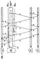
- the root node 2 returns a Grant signal G(2) to node 1 and asserts a Data Prefix signal D(2) on its other port, which is repeated by a node 3 as a Data Prefix signal D(3) to node 4.
- Nodes 3 and 4 change their state from A0 to RX.
- the Data Prefix DP(4) and the following Bus Reset are repeated by root node 2 as D(5) which is repeated by node 3 as D(6) to node 4.
- nodes 1, 2, and 3 assert idle signals I(8), I(9) and I(10), respectively, to start a Tree ID process (Fig. 2C).
- Node 1 shifts to TX by asserting a Data Prefix DP2 and changes to state R0 by signalling a Bus Request BR1 to node 2, resulting in the node 2 changing to state R0 by simultaneously asserting a Bus Request BR2 to nodes 1 and 3.
- Node 3 changes its state from RX to R0 by signalling a Bus Request BR3 to nodes 2 and 4.
- the short reset period of 1.3 ⁇ s expires at node 2, it changes state from R0 to R1 by signalling an idle state ID2 to nodes 1 and 3.
- the short reset time expires at node 2 and it changes from R0 to R1 by signalling an idle state ID3 to nodes 2 and 4.
- Root node 2 will change its state from R1 to R0 if the critical period of 1.46 ⁇ s expires. Since an idle or a parent notify signal should arrive a 1.46- ⁇ s period after the root node 2 changes to state R1 in order for it to reliably perform a short bus reset, the idle signal ID3 must arrive on node 2 within the 1.46- ⁇ s critical period after the short reset period of 1.3 ⁇ s.
- the idle state signal ID3 arrives on node 2 after the 1.46- ⁇ s critical period and the node 2 changes to state R0, rather than T0, and sets the bus reset to the long reset time.
- an idle state or a parent notify state should arrive within a total period of 2.76 ⁇ s after the node 2 asserted Bus Reset BR2 to node 3.
- the maximum turnaround time between two nodes is given by: 2 x 1.3 ⁇ s + 0.16 ⁇ s > 2 (cable delay + physical-layer delay) + 1.3 ⁇ s therefore, 1.3 ⁇ s + 0.16 ⁇ s > 2 (cable delay + physical-layer delay) If the physical-layer delay is 300 ns and the cable delay is 5 ns/meter, the cable length between two nodes must not exceed 78 meters.
- a transceiver circuit comprising a line transmitter for transmitting a signal from a higher layer to a transmission medium, a line receiver for receiving a signal from the transmission medium, a first detector for producing a first detector output if a first bus reset signal is detected in the signal transmitted from the line transmitter, and a second detector for producing a second detector output when the second bus reset signal is being detected in the received signal.
- Control circuitry is provided for normally applying the received signal to the higher layer.
- a selector is provided having a first position in which the selector is normally coupling the received signals to the higher layer and a second position in which the selector is coupling a masking signal to the higher layer.
- Control circuitry sets the selector in the second position in response to a start timing of the first detector output, starts a count operation for incrementing a count value in response to a start timing of the second detector output until the count value exceeds a predetermined value, and sets the selector in the first position in response to the end timing of the count operation.
- the present invention provides a method of performing a bus reset process, comprising the steps of (a) transmitting a signal to a transmission medium and receiving a signal therefrom, (b) applying the received signal to a higher layer, (c) detecting a transmit bus reset signal in said transmitted signal, (d) exclusively applying a masking signal to said higher layer in response to a start timing of the transmit bus reset signal, (e) detecting a receive bus reset signal in the received signal, (f) activating a count operation for incrementing a count value in response to a start timing of the receive bus reset signal until the count value exceeds a predetermined value, and (g) exclusively applying the received signal to said higher layer in response to an end timing of the count operation.
- a transceiver circuit of the IEEE-1394 standard can be used as a long-distance port of an IEEE-1394 network node, and includes an 8B/10B block encoder 11 for encoding a signal from a higher layer to coded parallel data, which is converted to a serial bit stream by a parallel-to-serial converter 12 for transmission to a serial bus whose length to an adjacent node is longer than 4.5 meters.
- the parallel data from the higher layer is further supplied to a transmit line state detector 13 for detecting data prefix signal, bus reset signal and signals other than bus reset and data prefix.
- signals from the serial bus are converted by a serial-to-parallel converter 14 to parallel data which is decoded by an 8B/10B decoder 15 for application to a receive line state detector 16 for detecting bus reset signal and non-bus reset signal.
- a time counter 17 is provided for receiving a bus reset signal detected by the RX line state detector 16 to continuously increment a count value during the presence of the detected bus reset signal and produces an output signal when the count value exceeds a threshold value of 1.3 ⁇ s.
- the time-out period of the counter 17 corresponds to the time taken to perform a bus reset.
- the output of the decoder 15 is also applied to a selector 18 which operates as a line-signal masking circuit for masking the state machine (higher layer) in response to a control signal from a selector controller 19.
- a pseudo-idle state signal is used for masking the state machine to prevent it from responding to received line state signals.
- Selector controller 19 receives the outputs of line state detectors 13 and 16 and the output of counter 17. Selector controller 19 operates according to a state diagram shown in Fig. 6.
- the state diagram has five states E0 to E4 which may be implemented by flip-flops 20 to 24 and state transitions are controlled by various logic gates 30 to 42.
- Fig. 6 Prior to describing the operation of the selector controller 19 of Fig. 5, reference is first made to Fig. 6.
- selector controller 19 When the selector controller 19 receives a signal from the TX-line state detector 13 indicating that a bus reset signal is received from the higher layer during state E0, it changes to state E1. Selector controller 19 returns to state E0 when either the TX line state detector 13 or the RX line state detector 16 detects a signal other than bus reset. If the TX line state detector 13 detects a data prefix signal, the controller 19 changes from E0 to E2, and then returns to E0 if the TX line state detector 16 detects a signal other than the TX-bus reset. A state transition from E2 to E3 occurs when the controller 19 receives a signal indicating that a TX-bus-reset signal is being detected by the TX line state detector 13 in data received from the higher layer.
- State E3 indicates the start timing of a masking control signal to be applied to the selector 18.
- Selector controller 19 maintains state E3 as long as it is receiving the TX-bus-reset indicating signal from the TX-line state detector 13.
- State transition from E3 to E4 takes place when the controller 19 receives a signal from the RX-line state detector 16 indicating that an RX-bus reset signal is being detected in the output of decoder 15.
- the RX-bus reset signal is a short bus reset (SBR) signal (i.e., 1.3 ⁇ s or smaller)
- the RX-line state detector 16 detects a signal other than bus reset at the end timing of the SBR signal and the controller 19 changes its state to E0.
- SBR short bus reset
- the E4-E0 state transition indicates the end timing of the masking signal. If the RX-bus reset signal is a long bus reset (LBR) signal (i.e., longer than 1.3 ⁇ s), the counter 17 produces an output signal that causes the controller 19 to change its state to E0.
- LBR long bus reset
- Controller 19 is initially set to E0 (Normal) by setting the flip-flop 20 and all other flip-flops in response to an internal reset signal.
- Selector 18 is conditioned to supply the output of decoder 15 to the higher layer.
- the AND gate 30 is enabled for responding to an RX-bus-reset indicating signal from the RX-line state detector 16 by setting the flip-flop 21.
- the output of flip-flop 21 is used to enable the AND gate 31 and to reset the flip-flop 20 through OR gate 32.
- the controller 19 changes its state from E0 (Normal) to E1 (Escape). If either line state detector detects a signal other than bus reset signal, the AND gate 31 is activated through OR gate 33, and the flip-flop 20 is set via OR gate 34, resulting in a state transition from E1 to E0.
- the AND gate 35 is ready to respond to a signal from the TX-line state detector 13, indicating that a data prefix signal is detected, for setting the flip-flop 22, while resetting the flip-flop 20 through OR gate 32 and enabling AND gates 36 and 37.
- Selector controller 19 changes its state from E0 to E2 (TX-Data Prefix), as shown in Fig. 7. If the TX-line state detector 13 detects a signal other than bus reset and data prefix signals, the AND gate 36 is rendered active, resetting the flip-flop 22 through OR gate 38 and setting the flip-flop 20 again, returning to state E0. If the TX-line state detector 13 detects a bus reset signal BR2 transmitted to the node 3 (Fig.
- the AND gate 37 is activated for setting the flip-flop 23 and resetting the flip-flop 22 through OR gate 38, changing state from E2 to E3 (TX-Reset).
- the output of flip-flop 23 is coupled through OR gate 39 to the selector 18 as the start timing of a masking signal.
- the selector 18 couples the idle state signal, instead of the output of decoder 15, to the higher layer.
- AND gate 40 is conditioned to set the flip-flop 24 in response to a signal from the RX-line state detector 16, indicating that a bus reset signal BR3 is arriving from the node 3. Controller 19 changes its state from E3 to E4 (RX Reset).
- the AND gate 41 is enabled to respond to the output of an OR gate 42 whose inputs are connected from the RX-line state detector 16 and the time counter 17.
- the output of flip-flop 24 is coupled through OR gate 39 to the selector 18 to continue the application of the idle state signal to the higher layer.
- AND gate 41 will be activated in response to the output of OR gate 42 if the time counter 17 produces a signal indicating that an RX-bus reset signal continues for a period longer than 1.3 ⁇ s, or the RX-line state detector 16 produces a signal indicating that a signal other than RX bus reset signal occurs during the time-out period of 1.3 ⁇ s.
- the AND gate 34 is activated, the flip-flop 24 is reset and the flip-flop 20 is set again through OR gate 34.
- Selector controller 19 now changes its state from E4 to E0 and the output of decoder 15 is coupled to the higher layer, instead of the idle state signal.
- the RX-line state detector 16 detects a signal other than bus reset and data prefix signals and the transition from E4 to E0 takes place at time t s prior to the time-out instant t 0 of time counter 17 (Fig.7). If the reset signal BR3 is a long bus reset (LBR), the counter 17 produces an output signal and the transition from E4 to E0 takes place at time t 0 which coincides with the time-out instant of time counter 17.
- SBR short bus reset
- LBR long bus reset
- Selector controller 19 and counter 17 may be implemented by a programmed routine stored in a storage medium, as shown in Fig. 8.
- a count variable C is set equal to zero at step 51, and the selector 18 is switched to the normal position for coupling the output of decoder 15 to the higher layer (step 52).
- the selector 54 is set in the masking position (step 54).
- the controller 19 starts incrementing the count variable C at step 56 and compares it to a threshold value that represents the time-out period of 1.3 ⁇ s (step 57).
- step 58 determines whether a signal other than bus reset is received by the RX-line state detector 16. If the decision at step 58 is negative, step 57 is repeated. If the decision at step 57 or 58 is affirmative, the controller 19 proceeds to step 59 to set the selector 18 in the normal position and then terminate the routine.
Landscapes
- Engineering & Computer Science (AREA)
- Theoretical Computer Science (AREA)
- Physics & Mathematics (AREA)
- General Engineering & Computer Science (AREA)
- General Physics & Mathematics (AREA)
- Small-Scale Networks (AREA)
- Computer Networks & Wireless Communication (AREA)
- Signal Processing (AREA)
- Communication Control (AREA)
Abstract
Description
Claims (19)
- A transceiver circuit comprising:a line transmitter (11, 12) for transmitting a signal from a higher layer to a transmission medium;a line receiver (14, 15) for receiving a signal from said transmission medium;a first detector (13) for producing a first detector output if a first bus reset signal is detected in the signal transmitted from said line transmitter;a second detector (16) for producing a second detector output when said second bus reset signal is being detected in the received signal;a selector (18) having a first position in which the selector is normally coupling the received signals to said higher layer and a second position in which the selector is coupling a masking signal to said higher layer; andcontrol circuitry (17, 19) for setting the selector in the second position in response to a start timing of said first detector output, starting a count operation for incrementing a count value in response to a start timing of the second detector output until the count value exceeds a predetermined value, and setting the selector in the first position in response to an end timing of the count operation.
- The circuit of claim 1, wherein said control circuitry is arranged to set the selector in the first position in response to an end timing of the second detector output if the same is earlier than the end timing of the count operation, or in response to the end timing of the count operation if the same is earlier than the end timing of the second detector output.
- The circuit of claim 1 or 2, wherein said masking signal is a pseudo-idle state signal.
- The circuit of claim 1, 2 or 3, wherein said first detector (13) is arranged to produce a third detector output if a data prefix signal is detected in the transmitted signal, and wherein said control circuitry (19) is arranged to:change from a first state (E0) to a second state (E1) in response to the second detector output for setting the selector (18) in said first position, and return from the second state (E1) to the first state (E0) in response to a signal other than said first and second detector outputs, and change from the first state (E0) to a third state (E2) in response to the third detector signal,return from the third state (E2) to the first state (E0) in response to a signal other than first and third detector outputs and change from the third state (E2) to a fourth state (E3) in response to said first detector output for setting said selector (18) in said second position, andchange from the fourth state (E3) to a fifth state (E4) in response to the second detector output, and change from the fifth state (E4) to the first state (E0) in response to the end timing of said count operation for setting the selector in the first position.
- The circuit of claim 1, 2, 3 or 4, wherein said predetermined value represents the length of time taken to perform a bus reset.
- The circuit of claim 1, 2, 3, 4 or 5, wherein said transmission medium is a serial bus and wherein said line transmitter includes an encoder (11) for coding the signals from said higher layer to a coded parallel signal and a parallel-to-serial converter (12) for converting the encoded parallel signal to an encoded serial signal for transmission to said serial bus, and said line receiver includes a serial-to-parallel converter (14) for converting a coded serial signal from the serial bus to a parallel coded signal and a decoder (15) for decoding the parallel coded signal to a parallel decoded signal for application to the first position of said selector (18).
- The circuit of claim 6, further comprising an IEEE-1394 interface connected to said serial bus.
- A communication system comprising:a plurality of nodes interconnected by transmission mediums;each of said nodes comprising:a line transmitter (11, 12) for transmitting a signal from a higher layer to a transmission medium;a line receiver (14, 15) for receiving a signal from said transmission medium;a first detector (13) for producing a first detector output if a first bus reset signal is detected in the signal transmitted from said line transmitter;a second detector (16) for producing a second detector output when said second bus reset signal is being detected in the received signal;a selector (18) having a first position in which the selector is normally coupling the received signals to said higher layer and a second position in which the selector is coupling a masking signal to said higher layer; andcontrol circuitry (17, 19) for setting the selector in the second position in response to a start timing of said first detector output, starting a count operation for incrementing a count value in response to a start timing of the second detector output until the count value exceeds a predetermined value, and setting the selector in the first position in response to an end timing of the count operation.
- The communication system of claim 8, wherein said control circuitry is arranged to set the selector in the first position in response to an end timing of the second detector output if the same is earlier than the end timing of the count operation, or in response to the end timing of the count operation if the same is earlier than the end timing of the second detector output.
- The system of claim 8 or 9, wherein said masking signal is a pseudo-idle state signal.
- The system of claim 8, 9 or 10, wherein said first detector (13) is arranged to produce a third detector output if a data prefix signal is detected in the transmitted signal, and wherein said control circuitry (19) is arranged to:change from a first state (E0) to a second state (E1) in response to the second detector output for setting the selector (18) in said first position, and return from the second state (E1) to the first state (E0) in response to a signal other than said first and second detector outputs, and change from the first state (E0) to a third state (E2) in response to the third detector signal,return from the third state (E2) to the first state (E0) in response to a signal other than first and third detector outputs and change from the third state (E2) to a fourth state (E3) in response to said first detector output for setting said selector (18) in said second position, andchange from the fourth state (E3) to a fifth state (E4) in response to the second detector output, and change from the fifth state (E4) to the first state (E0) in response to the end timing of said count operation for setting the selector in the first position.
- The system of claim 8, 9, 10 or 11, wherein said predetermined value represents the length of time taken to perform a bus reset.
- The communication system of claim 8, 9, 10, 11 or 12, wherein said transmission medium is a serial bus and wherein said line transmitter includes an encoder (11) for coding the signals from said higher layer to a coded parallel signal and a parallel-to-serial converter (12) for converting the encoded parallel signal to an encoded serial signal for transmission to said serial bus, and said line receiver includes a serial-to-parallel converter (14) for converting a coded serial signal from the serial bus to a parallel coded signal and a decoder (15) for decoding the parallel coded signal to a parallel decoded signal for application to the first position of said selector (18).
- The communication system of claim 13, wherein each of said nodes further comprises an IEEE-1394 interface connected to said serial bus.
- A method of performing a bus reset process, comprising the stepsa) transmitting a signal to a transmission medium and receiving a signal therefrom;b) applying the received signal to a higher layer;c) detecting a transmit bus reset signal in said transmitted signal;d) exclusively applying a masking signal to said higher layer in response to a start timing of the transmit bus reset signal;e) detecting a receive bus reset signal in the received signal;f) activating a count operation for incrementing a count value in response to a start timing of the receive bus reset signal until the count value exceeds a predetermined value; andg) exclusively applying the received signal to said higher layer in response to an end timing of the count operation.
- The method of claim 15, wherein the step (g) comprises the steps of exclusively applying the received signal to said higher layer in response to an end timing of the receive bus reset signal if the same is earlier than the end timing of the count operation, or in response to the end timing of the count operation if the same is earlier than the end timing of the second bus reset signal.
- A storage medium for storing a control program for performing a bus reset process, comprising the steps of:a) transmitting a signal to a transmission medium and receiving a signal therefrom;b) applying the received signal to a higher layer;c) detecting a transmit bus reset signal in said transmitted signal;d) exclusively applying a masking signal to said higher layer in response to a start timing of the transmit bus reset signal;e) detecting a receive bus reset signal in the received signal;f) activating a count operation for incrementing a count value in response to a start timing of the receive bus reset signal until the count value exceeds a predetermined value; andg) exclusively applying the received signal to said higher layer in response to an end timing of the count operation.
- The storage medium of claim 17, wherein the step (g) comprises the steps of exclusively applying the received signal to said higher layer in response to an end timing of the receive bus react signal if the same is earlier than the end timing of the count operation, or in response to the end timing of the count operation if the same is earlier than the end timing of the second bus reset signal.
- The storage medium of claim 17 or 18, wherein said masking signal is a pseudo-idle state signal.
Applications Claiming Priority (2)
| Application Number | Priority Date | Filing Date | Title |
|---|---|---|---|
| JP17616999A JP3289707B2 (en) | 1999-06-23 | 1999-06-23 | Transmission / reception circuit, transmission / reception method, and recording medium |
| JP17616999 | 1999-06-23 |
Publications (2)
| Publication Number | Publication Date |
|---|---|
| EP1063596A2 true EP1063596A2 (en) | 2000-12-27 |
| EP1063596A3 EP1063596A3 (en) | 2006-04-26 |
Family
ID=16008879
Family Applications (1)
| Application Number | Title | Priority Date | Filing Date |
|---|---|---|---|
| EP00113025A Withdrawn EP1063596A3 (en) | 1999-06-23 | 2000-06-21 | Circuit and method for reliably performing bus reset regardless of cable length |
Country Status (5)
| Country | Link |
|---|---|
| US (1) | US6529977B1 (en) |
| EP (1) | EP1063596A3 (en) |
| JP (1) | JP3289707B2 (en) |
| KR (1) | KR100352568B1 (en) |
| CN (1) | CN1196067C (en) |
Cited By (1)
| Publication number | Priority date | Publication date | Assignee | Title |
|---|---|---|---|---|
| EP1320036A3 (en) * | 2001-12-17 | 2007-06-20 | Matsushita Electric Industrial Co., Ltd. | Digital data processing device, bus controlling method, bus controlling program and recording medium |
Families Citing this family (12)
| Publication number | Priority date | Publication date | Assignee | Title |
|---|---|---|---|---|
| JP2001119410A (en) * | 1999-10-21 | 2001-04-27 | Sony Corp | Processing method in the self-identification phase |
| JP2001292146A (en) * | 2000-04-07 | 2001-10-19 | Sony Corp | Processing method for electronic equipment and digital serial data interface device in bus initialization phase |
| JP2001313646A (en) * | 2000-04-27 | 2001-11-09 | Sony Corp | Electronic apparatus and state control method for physical layer circuit thereof |
| JP2001345827A (en) * | 2000-06-02 | 2001-12-14 | Minolta Co Ltd | Interface device, node having the same, interface system, control method for bus reset and computer-readable recording medium recorded with control program for bus reset |
| US6870900B1 (en) * | 2000-06-16 | 2005-03-22 | Bellsouth Intellectual Property Corporation | Proactive maintenance application |
| US6687779B1 (en) * | 2000-07-14 | 2004-02-03 | Texas Instruments Incorporated | Method and apparatus for transmitting control information across a serialized bus interface |
| KR100401129B1 (en) * | 2001-04-20 | 2003-10-10 | 한국전자통신연구원 | A Digital Block Design Of Bus Arbitration In IEEE1394 Transceiver |
| DE10246895B3 (en) * | 2002-10-08 | 2004-06-09 | Siemens Ag | Procedure for changing a parameter for the operation of a network and participants for performing the procedure |
| DE102008004819B4 (en) * | 2008-01-17 | 2010-06-24 | Texas Instruments Deutschland Gmbh | Circuit and method for detecting network node aging in communication networks |
| CN108984458B (en) * | 2018-08-09 | 2021-10-29 | 哈尔滨诺信工大测控技术有限公司 | A custom serial open bus |
| CN113037428B (en) * | 2019-12-09 | 2022-01-25 | 大唐移动通信设备有限公司 | Data flow processing method and device |
| DE102020210096A1 (en) * | 2020-08-10 | 2022-02-10 | Robert Bosch Gesellschaft mit beschränkter Haftung | Method and device for determining information of a bus system |
Family Cites Families (4)
| Publication number | Priority date | Publication date | Assignee | Title |
|---|---|---|---|---|
| US4218759A (en) * | 1978-06-30 | 1980-08-19 | International Business Machines Corporation | Sync in-sync out calibration for cable length delays |
| EP1085701A3 (en) * | 1994-03-09 | 2001-07-04 | Matsushita Electric Industrial Co., Ltd. | Data transmission system and method |
| DE69621725T2 (en) * | 1995-03-29 | 2003-01-30 | Koninklijke Philips Electronics N.V., Eindhoven | SYSTEM FOR PROVIDING A DEFINED TIME REFERENCE BETWEEN INPUT AND OUTPUT OF DATA AND TRANSMITTERS AND RECEIVERS FOR SUCH A SYSTEM |
| US5764526A (en) * | 1996-04-08 | 1998-06-09 | Microsoft Corporation | Dynamic propagation delay calculation using an array of storage cells |
-
1999
- 1999-06-23 JP JP17616999A patent/JP3289707B2/en not_active Expired - Fee Related
-
2000
- 2000-06-21 EP EP00113025A patent/EP1063596A3/en not_active Withdrawn
- 2000-06-22 US US09/598,479 patent/US6529977B1/en not_active Expired - Lifetime
- 2000-06-23 KR KR1020000034686A patent/KR100352568B1/en not_active Expired - Fee Related
- 2000-06-23 CN CNB001094416A patent/CN1196067C/en not_active Expired - Fee Related
Cited By (1)
| Publication number | Priority date | Publication date | Assignee | Title |
|---|---|---|---|---|
| EP1320036A3 (en) * | 2001-12-17 | 2007-06-20 | Matsushita Electric Industrial Co., Ltd. | Digital data processing device, bus controlling method, bus controlling program and recording medium |
Also Published As
| Publication number | Publication date |
|---|---|
| JP3289707B2 (en) | 2002-06-10 |
| CN1196067C (en) | 2005-04-06 |
| CN1279429A (en) | 2001-01-10 |
| JP2001007827A (en) | 2001-01-12 |
| KR20010015057A (en) | 2001-02-26 |
| KR100352568B1 (en) | 2002-09-12 |
| EP1063596A3 (en) | 2006-04-26 |
| US6529977B1 (en) | 2003-03-04 |
Similar Documents
| Publication | Publication Date | Title |
|---|---|---|
| US6765923B1 (en) | Early arbitration on a full duplex bus | |
| EP0577778B1 (en) | Transceiver interface | |
| US5857075A (en) | Method and integrated circuit for high-bandwidth network server interfacing to a local area network | |
| US4332027A (en) | Local area contention network data communication system | |
| JP3159144B2 (en) | Transmitter / receiver circuit | |
| US6529977B1 (en) | Circuit and method for reliably performing bus reset regardless of cable length | |
| EP0459753A2 (en) | Network access controller having logical FIFO buffer | |
| WO1999039479A1 (en) | Distributed arbitration on a full duplex bus | |
| JPH04270529A (en) | Repeater and its manufacture | |
| US6600755B1 (en) | Link technology detection in multiple speed physical links | |
| JPS63175549A (en) | Poling | |
| EP1987631B1 (en) | Method and device to transmit a busy medium signal to another device | |
| US4989203A (en) | Apparatus for providing multiple controller interfaces to a standard digital modem and including separate contention resolution | |
| JP3277887B2 (en) | Transmission / reception method, transmission / reception circuit and method for controlling transmission / reception circuit | |
| US4993023A (en) | Apparatus for providing multiple controller interfaces to a standard digital modem and including multiplexed contention resolution | |
| US4835776A (en) | Communication filter | |
| US5729547A (en) | Automatic driver/receiver control for half-duplex serial networks | |
| KR100567309B1 (en) | How to Improve Bus Usage Through Data Header Error Checking | |
| RU126162U1 (en) | COMMUNICATION INTERFACE DEVICE FOR NETWORK Space Wire | |
| US7145915B1 (en) | Circuit and method for exchanging signals between network nodes | |
| US5898842A (en) | Network controller adapter that prevents loss of data received or transmitted | |
| RU2483351C1 (en) | COMMUNICATION INTERFACE DEVICE FOR SpaceWire NETWORK | |
| US4843605A (en) | Node apparatus for communication network having multi-conjunction architecture | |
| US7889658B1 (en) | Method of and system for transferring overhead data over a serial interface | |
| Donchev et al. | Implementation of CAN controller with FPGA structures |
Legal Events
| Date | Code | Title | Description |
|---|---|---|---|
| PUAI | Public reference made under article 153(3) epc to a published international application that has entered the european phase |
Free format text: ORIGINAL CODE: 0009012 |
|
| AK | Designated contracting states |
Kind code of ref document: A2 Designated state(s): AT BE CH CY DE DK ES FI FR GB GR IE IT LI LU MC NL PT SE |
|
| AX | Request for extension of the european patent |
Free format text: AL;LT;LV;MK;RO;SI |
|
| PUAL | Search report despatched |
Free format text: ORIGINAL CODE: 0009013 |
|
| AK | Designated contracting states |
Kind code of ref document: A3 Designated state(s): AT BE CH CY DE DK ES FI FR GB GR IE IT LI LU MC NL PT SE |
|
| AX | Request for extension of the european patent |
Extension state: AL LT LV MK RO SI |
|
| 17P | Request for examination filed |
Effective date: 20060317 |
|
| 17Q | First examination report despatched |
Effective date: 20060906 |
|
| AKX | Designation fees paid |
Designated state(s): DE FR GB NL |
|
| STAA | Information on the status of an ep patent application or granted ep patent |
Free format text: STATUS: THE APPLICATION IS DEEMED TO BE WITHDRAWN |
|
| 18D | Application deemed to be withdrawn |
Effective date: 20110104 |