EP1063568B1 - Method of forming a fine pattern and method of manufacturing a semiconductor device - Google Patents
Method of forming a fine pattern and method of manufacturing a semiconductor device Download PDFInfo
- Publication number
- EP1063568B1 EP1063568B1 EP00112783A EP00112783A EP1063568B1 EP 1063568 B1 EP1063568 B1 EP 1063568B1 EP 00112783 A EP00112783 A EP 00112783A EP 00112783 A EP00112783 A EP 00112783A EP 1063568 B1 EP1063568 B1 EP 1063568B1
- Authority
- EP
- European Patent Office
- Prior art keywords
- silicon
- film
- pattern
- forming
- sih
- Prior art date
- Legal status (The legal status is an assumption and is not a legal conclusion. Google has not performed a legal analysis and makes no representation as to the accuracy of the status listed.)
- Expired - Lifetime
Links
Images


Classifications
-
- H—ELECTRICITY
- H10—SEMICONDUCTOR DEVICES; ELECTRIC SOLID-STATE DEVICES NOT OTHERWISE PROVIDED FOR
- H10P—GENERIC PROCESSES OR APPARATUS FOR THE MANUFACTURE OR TREATMENT OF DEVICES COVERED BY CLASS H10
- H10P76/00—Manufacture or treatment of masks on semiconductor bodies, e.g. by lithography or photolithography
-
- H—ELECTRICITY
- H10—SEMICONDUCTOR DEVICES; ELECTRIC SOLID-STATE DEVICES NOT OTHERWISE PROVIDED FOR
- H10P—GENERIC PROCESSES OR APPARATUS FOR THE MANUFACTURE OR TREATMENT OF DEVICES COVERED BY CLASS H10
- H10P14/00—Formation of materials, e.g. in the shape of layers or pillars
- H10P14/60—Formation of materials, e.g. in the shape of layers or pillars of insulating materials
- H10P14/69—Inorganic materials
- H10P14/692—Inorganic materials composed of oxides, glassy oxides or oxide-based glasses
- H10P14/6921—Inorganic materials composed of oxides, glassy oxides or oxide-based glasses containing silicon
- H10P14/69215—Inorganic materials composed of oxides, glassy oxides or oxide-based glasses containing silicon the material being a silicon oxide, e.g. SiO2
-
- G—PHYSICS
- G03—PHOTOGRAPHY; CINEMATOGRAPHY; ANALOGOUS TECHNIQUES USING WAVES OTHER THAN OPTICAL WAVES; ELECTROGRAPHY; HOLOGRAPHY
- G03F—PHOTOMECHANICAL PRODUCTION OF TEXTURED OR PATTERNED SURFACES, e.g. FOR PRINTING, FOR PROCESSING OF SEMICONDUCTOR DEVICES; MATERIALS THEREFOR; ORIGINALS THEREFOR; APPARATUS SPECIALLY ADAPTED THEREFOR
- G03F7/00—Photomechanical, e.g. photolithographic, production of textured or patterned surfaces, e.g. printing surfaces; Materials therefor, e.g. comprising photoresists; Apparatus specially adapted therefor
- G03F7/004—Photosensitive materials
- G03F7/09—Photosensitive materials characterised by structural details, e.g. supports, auxiliary layers
- G03F7/091—Photosensitive materials characterised by structural details, e.g. supports, auxiliary layers characterised by antireflection means or light filtering or absorbing means, e.g. anti-halation, contrast enhancement
-
- G—PHYSICS
- G03—PHOTOGRAPHY; CINEMATOGRAPHY; ANALOGOUS TECHNIQUES USING WAVES OTHER THAN OPTICAL WAVES; ELECTROGRAPHY; HOLOGRAPHY
- G03F—PHOTOMECHANICAL PRODUCTION OF TEXTURED OR PATTERNED SURFACES, e.g. FOR PRINTING, FOR PROCESSING OF SEMICONDUCTOR DEVICES; MATERIALS THEREFOR; ORIGINALS THEREFOR; APPARATUS SPECIALLY ADAPTED THEREFOR
- G03F7/00—Photomechanical, e.g. photolithographic, production of textured or patterned surfaces, e.g. printing surfaces; Materials therefor, e.g. comprising photoresists; Apparatus specially adapted therefor
- G03F7/16—Coating processes; Apparatus therefor
-
- H—ELECTRICITY
- H10—SEMICONDUCTOR DEVICES; ELECTRIC SOLID-STATE DEVICES NOT OTHERWISE PROVIDED FOR
- H10P—GENERIC PROCESSES OR APPARATUS FOR THE MANUFACTURE OR TREATMENT OF DEVICES COVERED BY CLASS H10
- H10P14/00—Formation of materials, e.g. in the shape of layers or pillars
- H10P14/60—Formation of materials, e.g. in the shape of layers or pillars of insulating materials
- H10P14/63—Formation of materials, e.g. in the shape of layers or pillars of insulating materials characterised by the formation processes
- H10P14/6326—Deposition processes
- H10P14/6328—Deposition from the gas or vapour phase
- H10P14/6334—Deposition from the gas or vapour phase using decomposition or reaction of gaseous or vapour phase compounds, i.e. chemical vapour deposition
-
- H—ELECTRICITY
- H10—SEMICONDUCTOR DEVICES; ELECTRIC SOLID-STATE DEVICES NOT OTHERWISE PROVIDED FOR
- H10P—GENERIC PROCESSES OR APPARATUS FOR THE MANUFACTURE OR TREATMENT OF DEVICES COVERED BY CLASS H10
- H10P14/00—Formation of materials, e.g. in the shape of layers or pillars
- H10P14/60—Formation of materials, e.g. in the shape of layers or pillars of insulating materials
- H10P14/63—Formation of materials, e.g. in the shape of layers or pillars of insulating materials characterised by the formation processes
- H10P14/6326—Deposition processes
- H10P14/6328—Deposition from the gas or vapour phase
- H10P14/6334—Deposition from the gas or vapour phase using decomposition or reaction of gaseous or vapour phase compounds, i.e. chemical vapour deposition
- H10P14/6336—Deposition from the gas or vapour phase using decomposition or reaction of gaseous or vapour phase compounds, i.e. chemical vapour deposition in the presence of a plasma [PECVD]
-
- H—ELECTRICITY
- H10—SEMICONDUCTOR DEVICES; ELECTRIC SOLID-STATE DEVICES NOT OTHERWISE PROVIDED FOR
- H10P—GENERIC PROCESSES OR APPARATUS FOR THE MANUFACTURE OR TREATMENT OF DEVICES COVERED BY CLASS H10
- H10P14/00—Formation of materials, e.g. in the shape of layers or pillars
- H10P14/60—Formation of materials, e.g. in the shape of layers or pillars of insulating materials
- H10P14/65—Formation of materials, e.g. in the shape of layers or pillars of insulating materials characterised by treatments performed before or after the formation of the materials
- H10P14/6516—Formation of materials, e.g. in the shape of layers or pillars of insulating materials characterised by treatments performed before or after the formation of the materials of treatments performed after formation of the materials
- H10P14/6529—Formation of materials, e.g. in the shape of layers or pillars of insulating materials characterised by treatments performed before or after the formation of the materials of treatments performed after formation of the materials by exposure to a gas or vapour
- H10P14/6532—Formation of materials, e.g. in the shape of layers or pillars of insulating materials characterised by treatments performed before or after the formation of the materials of treatments performed after formation of the materials by exposure to a gas or vapour by exposure to a plasma
-
- H—ELECTRICITY
- H10—SEMICONDUCTOR DEVICES; ELECTRIC SOLID-STATE DEVICES NOT OTHERWISE PROVIDED FOR
- H10P—GENERIC PROCESSES OR APPARATUS FOR THE MANUFACTURE OR TREATMENT OF DEVICES COVERED BY CLASS H10
- H10P14/00—Formation of materials, e.g. in the shape of layers or pillars
- H10P14/60—Formation of materials, e.g. in the shape of layers or pillars of insulating materials
- H10P14/66—Formation of materials, e.g. in the shape of layers or pillars of insulating materials characterised by the type of materials
- H10P14/668—Formation of materials, e.g. in the shape of layers or pillars of insulating materials characterised by the type of materials the materials being characterised by the deposition precursor materials
- H10P14/6681—Formation of materials, e.g. in the shape of layers or pillars of insulating materials characterised by the type of materials the materials being characterised by the deposition precursor materials the precursor containing a compound comprising Si
- H10P14/6682—Formation of materials, e.g. in the shape of layers or pillars of insulating materials characterised by the type of materials the materials being characterised by the deposition precursor materials the precursor containing a compound comprising Si the compound being a silane, e.g. disilane, methylsilane or chlorosilane
-
- G—PHYSICS
- G03—PHOTOGRAPHY; CINEMATOGRAPHY; ANALOGOUS TECHNIQUES USING WAVES OTHER THAN OPTICAL WAVES; ELECTROGRAPHY; HOLOGRAPHY
- G03F—PHOTOMECHANICAL PRODUCTION OF TEXTURED OR PATTERNED SURFACES, e.g. FOR PRINTING, FOR PROCESSING OF SEMICONDUCTOR DEVICES; MATERIALS THEREFOR; ORIGINALS THEREFOR; APPARATUS SPECIALLY ADAPTED THEREFOR
- G03F7/00—Photomechanical, e.g. photolithographic, production of textured or patterned surfaces, e.g. printing surfaces; Materials therefor, e.g. comprising photoresists; Apparatus specially adapted therefor
- G03F7/004—Photosensitive materials
- G03F7/0045—Photosensitive materials with organic non-macromolecular light-sensitive compounds not otherwise provided for, e.g. dissolution inhibitors
Definitions
- the present invention relates to a method of forming a fine pattern in a semiconductor device, and a method of manufacturing a semiconductor device having a fine pattern.
- a reduction-projection exposing technique has been widely used for fabricating a circuit pattern, such as an LSI.
- An improvement in resolution ascribable to a reduction in the wavelength of exposing radiation has recently been fostered in the field of exposure techniques.
- Resolution on the order of 0.1 ⁇ m is considered to become feasible as a result of employment of an ArF excimer laser (having a wavelength of 193 nm) in place of a KrF excimer laser (having a wavelength of 248 nm) which has been widely used.
- use of the X-ray lithography technique or electron beam lithography technique is under study in an attempt to form a finer pattern.
- a typical problems pertaining to a chemically-amplified resist is an anomaly in the cross section of each of patterns formed on various underlying films.
- an underlying film is a film containing nitrogen atoms, such as silicon nitride or titanium nitride
- a tapered portion appearing at the foot of a chemically-amplified resist pattern poses a serious problem.
- a silicon nitride film has been widely used as an etching mask or an inorganic antireflection film. Patterning is indispensable for nitride-film-based material, and an anomaly of pattern geometry, such as a tapering pattern, must be avoided.
- Such an anomaly of pattern geometry has been thought to be attributable to the phenomenon of acid being trapped by ammonium residing on the surface of a nitride film or by ammonium contaminated in the environment or being trapped by the lone pair of electrons of each nitrogen atom contained in a nitride film.
- a method of oxidizing the surface of a silicon nitride film through use of oxygen plasma has been proposed as described, for example, in Japanese Patent Application Laid-Open Nos. 83786/1996 and 134867/1997 , and a method of depositing a silicon oxide film on a silicon nitride film has been proposed as described in Japanese Patent Application Laid-Open No. 10-189441 .
- the experiments conducted by the inventor of the present invention has shown that the geometry of a resist pattern may be deteriorated even when the substrate laid immediately below a resist is subjected to the foregoing processing.
- the present inventor has examined the cause of the anomaly. As a result, the inventor has found that in a case where a high-resolution chemically-amplified resist is adopted, the geometry of a resist pattern is deteriorated even when nitrogen atoms are present in a trace amount on the surface of a silicon oxide film. The deterioration is considered to stem from acid being trapped by the lone pair of electrons of each nitrogen atom which is present on the surface of a substrate.
- nitrogen-containing components must be eliminated from a source gas during the course of a CVD operation.
- a source gas For example, use of the plasma CVD technique and use of silane and oxygen as source gases are desirable.
- silane and oxygen are used, reaction readily proceeds at ordinary temperatures even if no plasma exists, thereby producing a fine powder of SiO 2 in a chamber or a process gas inlet pipe. The resultant powder leads to the presence of particles on a wafer and is not desirable.
- a silicon oxide film be formed in only a plasma generation area without involvement of generation of particles while using, as an oxidizing gas, N 2 O or NO which would induce reaction only with the assistance of energy, such as that provided by plasma.
- a semiconductor device which comprises a substrate, an underlying layer, an anti-reflective coating of silicon oxynitride, a capping layer of low nitrogen content material such as silicon oxide, and a photoresist layer.
- This object is solved by a method of forming a fine pattern according to the independent claim 1 and by a method of manufacturing a semiconductor device according to the independent claim 3.
- FIGS. 1A through 3B and Table 1 A method of forming a fine pattern is described by reference to FIGS. 1A through 3B and Table 1.
- FIGS. 1A through 1C are schematic representations for describing processes of a method of forming a fine pattern employed in Examples 1 through 2 of the first embodiment and in Comparative Examples 1 through 5. Further, Table 1 provides requirements and results of the method of forming a fine pattern employed in Examples 1 through 2 and in Comparative Examples 1 through 5.
- reference numeral 1 designates a photoresist
- 1a designates a photoresist pattern
- 2 designates an oxide silicon film
- 3 designates a silicon nitride oxide film (SiON film)
- 4 designates a silicon substrate
- 5 designates a mask to be used for exposing the photoresist 1
- 6 designates exposing radiation.
- an SiON film 3 is deposited on the substrate 4 to a thickness of 25 nm through plasma CVD, and a silicon oxide film 2 is formed on the SiON film 3 to a thickness of 10 nm.
- Table 1 shows requirements for producing silicon oxide films employed in Examples 1 through 2 and requirements for producing silicon oxide films employed in Comparative examples 1 through 5.
- the present embodiment employs a parallel plate plasma enhanced CVD system (Eagle-10 by Japan ASM) and certain settings; that is, an RF frequency of 13.56 MHz, RF power of 350 W, and an internal chamber pressure of 380 Pa. Further, a prototype thermal CVD system (by TOKYO Electron) is used in the present embodiment.
- the photoresist 1 was formed by means of spin coating after deposition of a silicon oxide film 2.
- the step of coating photoresist is as follows. A substrate having the silicon oxide film 2 formed thereon was exposed to a hexamethyldisilazane (HMDS) atmosphere at a temperature of 90°C for 60 seconds. Subsequently, polyacryl-based positive ArF resist (AX-100, Clariant) was applied to the substrate to a thickness of 480 nm through spin-coating, and the substrate was heated on a hot plate at 115°C for 90 seconds.
- HMDS hexamethyldisilazane
- the wafer was exposed to exposing radiation 6 through a mask 5 by means of a prototype ArF excimer laser stepper (by ISI), wherewith a pattern was transferred onto the wafer.
- the exposure system has a numerical aperture of 0.6 and a ⁇ of 0.7.
- the wafer was heated on a hot plate at 110°C for 60 seconds and developed by means of the puddle developing technique while an organic alkaline solution, such as a tetramethylammoniumhydroxyde solution, was used as a developer solution.
- an organic alkaline solution such as a tetramethylammoniumhydroxyde solution
- FIGS. 3A and 3B are illustrations showing a difference in cross section between the resist patterns of 150 nm width formed in Examples 1 through 4 and those formed in Comparative Examples 1 through 4.
- FIG. 3A shows the cross section of one of the resist patterns formed in Examples 1 through 2
- FIG. 3B shows the cross section of one of the resist patterns formed in Comparative Examples 1 through 5.
- the resist pattern according to Examples 1 through 2 forms a substantially-right-angle corner at the foot of the resist pattern with respect to the substrate, and it is understood that a resist pattern has been correctly formed.
- the resist pattern according to Comparative Examples 1 through 5 shown in FIG. 3B forms a tapered corner or a curved corner at the foot of the resist pattern with respect to the substrate. Such a pattern is not desirable, because the dimensional accuracy of a resist pattern is deteriorated.
- the present inventor has defined the degree of a tapered corner at the foot of the resist pattern as shown in FIG. 2, thereby quantifying the accuracy of the resist pattern.
- reference symbol Wb denotes the width of a resist line formed in the boundary surface between a resist and a substrate; and Wm denotes the width of the resist line at a position elevated H/4 from the boundary surface.
- H denotes the height of the resist line.
- Wm denotes the width of the resist line at a position elevated 120 nm from the boundary surface.
- Table 1 shows results of measurement of a tapered corner of a resist pattern. As is evident from Table 1, so long as the concentration of nitrogen atoms which are present on the surface of a silicon oxide film is 0.1 atm.% or less, a tapered corner of a resist pattern is found to become small. In the present embodiment, the concentration of nitrogen atoms which are contained in a silicon oxide film and nitrogen atoms which are present on the surface of a silicon oxide film were measured through use of the Secondary Ion Mass Spectroscopy (SIMS) technique.
- SIMS Secondary Ion Mass Spectroscopy
- ArF excimer laser reduction exposure has been used for transferring a mask pattern through exposure
- another exposure technique may be employed.
- an X-ray exposure technique a KrF excimer laser contact exposure or reduction projection exposure technique, an F 2 excimer laser contact exposure or reduction projection exposure technique, a step-and-scan reflection-type reduction projection exposure technique using UV radiation as the light source, or a soft-X-ray exposure technique.
- the value of numerical aperture and the value of ⁇ are not limited to those described previously.
- a pattern to be exposed is not limited to a line pattern, and a hole pattern or a dot pattern may also be used as an object of exposure.
- Examples 1 through 2 and in Comparative Examples 1 through 5 a wafer was exposed to an HMDS atmosphere immediately before coating with a resist film, thus forming a contacting layer. In a case where a resist film is in sufficient contact with a substrate, formation of a contacting layer may be omitted.
- an silicon oxynitride film is deposited immediately beneath a silicon oxide film.
- a silicon nitride film may be deposited immediately beneath the silicon oxide film.
- the silicon oxide nitride film or the silicon nitride film may not be deposited.
- silane was used as a source gas.
- Si 2 H 6 , SiH 3 (CH 3 ), SiH 2 (CH 3 ) 2 , SiCl 2 H 2 , siCl 4 , or SiH(CH 3 ) 3 may be use.
- N 2 O was used as another source gas in Examples 1 through 3 and in Comparative Examples 1 through 4. However, NO or CO may be used.
- a fine resist pattern 1a has been formed as shown in FIG. 1C
- the underlying silicon oxide film 2 or the silicon oxide film 2 and the SiON film 3 are etched by way of the resist pattern 1a, thereby forming a fine pattern from an insulating film.
- a fine pattern can be formed from a conductive film.
- a semiconductor device can be manufactured through succeeding manufacturing processes, and explanation of manufacture of a semiconductor device is omitted.
- a semiconductor device having a pattern on the order of 0.1 ⁇ m can be fabricated, and the present invention can be usually preferably applied to formation of a pattern of 0.18 ⁇ m or less.
- a silicon-oxide-based film whose surface has a nitrogen content of 0.1 atm.% or less is formed, and a chemically-amplified photoresist is formed on the silicon-oxide-based film, thus constituting a resist pattern.
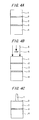
- FIGS. 4A through 4C are schematic representations for describing processes for forming a fine pattern, the processes being employed in Examples 3 through 5 and Comparative Examples 6 through 10.
- Table 2 provides requirements and results of the method of forming a fine pattern employed in Examples 3 through 5 and in Comparative Examples 6 through 10.
- reference numerals 1 through 6 and 1a are identical with those employed in FIG. 1 pertaining to the first embodiment, and hence repetition of their explanations is omitted.
- reference numeral 7 designates a BPSG film.
- a SiON film 3 is deposited to a thickness of 25 nm on the substrate 4 by means of the plasma CVD technique, and a BPSG film 7 was formed on the SiON film 3 to a thickness of 700 nm by means of the atmospheric pressure CVD technique.
- a silicon oxide film 2 was deposited on the BPSG film 7 to a thickness of 10 nm by means of the plasma CVD technique.
- the present embodiment employed a prototype plasma CVD system (of a parallel plate plasma enhanced CVD type, manufactured by Japan ASM).
- a substrate having the silicon oxide film 2 formed thereon was exposed to a hexamethyldisilazane (HMDS) atmosphere at a temperature of 90°C for 60 seconds.
- HMDS hexamethyldisilazane
- PAR-101 polyacryl-based positive ArF resist
- the wafer was exposed to exposing radiation 6 through a mask 5 and by means of a prototype ArF excimer laser stepper (by ISI), wherewith a pattern was transferred onto the wafer.
- An exposure system has a numerical aperture of 0.6 and a ⁇ of 0.7.
- the wafer was heated on a hot plate at 120°C for 60 seconds and developed by means of the puddle developing technique while an organic alkaline solution, such as a tetramethylammoniumhydroxyde solution, was used as a developer solution. As shown in FIG. 4C, a resist pattern (line pattern) 1a having a width of 150 nm was formed.
- an organic alkaline solution such as a tetramethylammoniumhydroxyde solution
- FIGS. 3A and 3B are illustrations showing a difference in cross section between the resist patterns of 150 nm width formed in Examples 1 through 5 and those formed in Comparative Examples 1 through 10.
- the resist pattern according to Examples 3 through 5 forms a substantially-right-angle corner with respect to the substrate in the vicinity of the area between the substrate and the resist pattern as shown in FIG. 3A, and it is understood that a resist pattern has been correctly formed.
- the resist pattern according to Comparative Examples 6 through 10 forms a tapered corner with respect to the substrate as shown in FIG. 3B.
- Such a pattern having a tapered corner is not desirable, because the dimensional accuracy of a resist pattern is deteriorated.
- ArF excimer laser reduction exposure has been used for transferring a mask pattern through exposure
- another exposure technique may be employed.
- an X-ray exposure technique a KrF excimer laser contact exposure or reduction projection exposure technique, an F 2 excimer laser contact exposure or reduction projection exposure technique, a step-and-scan reflection-type reduction projection exposure technique using UV radiation as the light source, or a soft-X-ray exposure technique.
- the value of numerical aperture and the value of ⁇ are not limited to those described previously.
- a pattern to be exposed is not limited to a line pattern, and a hole pattern or a dot pattern may also be used as an object of exposure.
- Examples 3 through 5 and in Comparative Examples 8 through 10 a wafer was exposed to an HMDS atmosphere immediately before coating with a resist film, thus forming a contacting layer. In a case where a resist film is in sufficient contact with a substrate, formation of a contacting layer may be omitted.
- the BPSG film 7 and the silicon oxynitride film 3 are deposited immediately beneath the silicon oxide film 2.
- these layers may be replaced with another material; for example, a BPSG film or a TEOS film.
- the SiON film may be replaced with a silicon-oxide-based film, or such layer may not be deposited.
- silane was used as a source gas.
- Si 2 H 6 , SiH 3 (CH 3 ), SiH 2 (CH 3 ) 2 , SiCl 2 H 2 , SiCl 4 , or SiH(CH 3 ) 3 may be used.
- N 2 O was used as another source gas in Examples 3 through 5. However NO or CO may be used.
- a silicon-oxide-based film whose surface has a nitrogen content of 0.1 atm.% or less is formed by means of setting a reaction temperature employed in the plasma CVD process to a value of 500°C or more, and a chemically-amplified photoresist is formed on the silicon-oxide-based film, thus constituting a resist pattern.
- FIGS. 1A through 1C are schematic representations for describing processes of a method of forming a fine pattern employed in Examples 6 through 8 of the third embodiment and in Comparative Examples 13 and 16. Further, Table 3 provides requirements and results of the method of forming a fine pattern employed in Examples 6 through 8 and Comparative Examples 13 and 16. Since FIGS. 1A through 1C have already been described in connection with the first embodiment, repetition of their explanations is omitted here.
- Examples 6 through 8 and in Comparative Examples 13 and 16 are identical with that employed in Examples 1 through 2 and in Comparative Examples 1 through 5 according to the first embodiment.
- Examples 6 through 7 are characterized by inserting, into the processes, a step of exposing the surface of a silicon oxide film to oxygen plasma or N 2 O plasma after formation of the silicon oxide film.
- Comparative Examples 13 and 16 are characterized by means of omission, from the processes, of the step of exposing a silicon oxide film to plasma, or by using a thermal CUD process.
- the SiON film 3 shown in FIG. 1 assumes a thickness of 100 nm, and the silicon oxide film 2 assumes a thickness of 30 nm.
- the present embodiment employed a plasma CVD system (Eagle-10, by Japan ASM) and certain settings: an RF frequency of 13.56 MHz; an RF power of 400 W, and an internal chamber pressure of 400 Pa.
- the surface of the silicon oxide film was subjected to treatment within the chamber that has been employed in the process of forming the silicon oxide film. More specifically, after completion of the process of forming a silicon oxide film, the gas to be introduced was changed to solely O 2 or N 2 O, and the processing operation was carried out continuously for about 60 seconds. At this time, a flow rate of N 2 O or O 2 was set to 1500 sccm, and the internal pressure of the chamber was set to 400 Pa.
- a silicon oxide film was coated with the photoresist 1.
- a process of coating a silicon oxide film with photoresist will now be described in detail.
- a substrate having the silicon oxide film 2 formed thereon was exposed to a hexamethyldisilazane (HMDS) atmosphere at a temperature of 90° for 60 seconds.
- HMDS hexamethyldisilazane
- a polynorbornane-based positive ArF resist by Shinetsu Chemical
- the wafer was exposed to exposing radiation 6 through a mask 5 and by means of a prototype ArF excimer laser stepper (NSR-S302A, by Nikon), wherewith a pattern was transferred onto the wafer.
- An exposure system has a numerical aperture of 0.6 and a ⁇ of 0.7.
- the wafer was heated on a hot plate at 110°C for 60 seconds and developed by means of the puddle developing technique while an organic alkaline solution, such as a tetramethylammoniumhydroxyde solution, was used as a developer solution.
- a resist pattern (line pattern) 1a having a width of 150 nm was formed.
- the thus-formed resist pattern 1a was observed through use of a scanning electron microscope (S-5000, by Hitachi), and the degree of a tapered corner of a resist pattern was quantified through use of the definition illustrated in FIG. 2.
- Table 3 shows observation results. A nitrogen content of the surface of a silicon oxide film was diminished by means of the wafer being subjected to a plasma atmosphere of oxidizing gas of O 2 or N 2 O, wherewith the degree of a tapered corner could be diminished. Control of pattern geometry has been further improved as a result of a reduction in the degree of a tapered corner of the photoresist.
- ArF excimer laser reduction exposure has been used for transferring a resist pattern through exposure
- another exposure technique may be employed.
- an X-ray exposure technique a KrF excimer laser contact exposure or reduction projection exposure technique, an F 2 excimer laser contact exposure or reduction projection exposure technique, a step-and-scan reflection-type reduction projection exposure technique using UV radiation as the light source, or a soft X-ray exposure technique.
- the value of numerical aperture and the value of ⁇ are not limited to those described previously.
- a pattern to be exposed is not limited to a line pattern, and a hole pattern or a dot pattern may also be used as an object of exposure.
- Examples 6 through 7 a wafer was exposed to an HMDS atmosphere immediately before coating with a resist film, thus forming a contact layer. In a case where a resist film is in sufficient contact with a substrate, formation of a contact layer may be omitted.
- a silicon oxynitride film is deposited immediately beneath a silicon oxide film.
- a silicon nitride film may be deposited in place of a silicon oxynitride film. Further, deposition of a silicon oxynitride film may not be required.
- Examples 6 through 7 Although in the present embodiment a parallel plate plasma enhanced CVD system was used in Examples 6 through 7, an ECR plasma CVD system or a bias ECR plasma CVD system may be used.
- a parallel plate plasma enhanced CVD system was used for treating the surface of a silicon oxide film
- an ECR plasma etching system or an asher may also be employed.
- N 2 O and O 2 were used for treating the surface of a silicon oxide film
- other oxidizing gas such as CO or NO, can be employed.
- silane was used as a source gas.
- Si 2 H 6 , SiH 3 (CH 3 ),SiH 2 (CH 3 ) 2 , SiCl 2 H 2 , SiCl 4 , or SiH(CH 3 ) 3 may be used.
- a silicon-oxide-based film whose surface has a nitrogen content of 0.1 atm.% or less is formed, and the surface of the silicon-oxide-based film is exposed to plasma atmosphere of oxidizing gas, such as oxygen or N 2 O, after formation of the silicon-oxide-based film, to thereby diminish the nitrogen content of the surface of the silicon oxide film.
- oxidizing gas such as oxygen or N 2 O
- a chemically-amplified photoresist is applied to the silicon oxide film by means of coating, thus forming a resist pattern.
- a silicon-oxide-based film is formed on a substrate.
- the silicon-oxide-based film may be formed directly or indirectly on an underlying layer, and a fine pattern is ultimately formed in the underlying layer through a fine resist pattern.
- a silicon-oxide-based film is directly formed on a substrate or by way of another layer on a substrate.
- a chemically-amplified photoresist is formed on the silicon-oxide-based film.
- a mask pattern is transferred onto the chemically-amplified photoresist upon exposure through a mask.
- nitrogen content of the surface of the silicon-oxide-based film is made to assume a value of 0.1 atm.% or less. Therefore, a highly-accurate fine pattern can be formed in a lithography step.
- Plasma CVD is employed during the course of the step of depositing the silicon-oxide-based film, and the silicon-oxide-based film is formed while the temperature at which the substrate is to be disposed is set to 500°C or more. Accordingly, nitrogen atoms contained in a silicon oxide film and those contained in the surface of the silicon oxide film can be reduced in amount. Deterioration in geometry of a resist pattern is prevented, thus enabling formation of a highly-accurate fine pattern.
- a step of exposing the surface of the silicon oxide film to plasma atmosphere of O 2 or N 2 O is added so as to follow the step of depositing the silicon-oxide-based film, whereby nitrogen content of the surface of the silicon oxide film can be diminished. Therefore, deterioration in geometry of a resist pattern is prevented, thus enabling formation of a highly-accurate fine pattern.
- a highly-accurate fine insulating or conductive pattern can be formed, and a semiconductor device having such a fine pattern can be fabricated.
Landscapes
- Physics & Mathematics (AREA)
- General Physics & Mathematics (AREA)
- Engineering & Computer Science (AREA)
- Architecture (AREA)
- Structural Engineering (AREA)
- Materials For Photolithography (AREA)
- Formation Of Insulating Films (AREA)
- Exposure Of Semiconductors, Excluding Electron Or Ion Beam Exposure (AREA)
- Exposure And Positioning Against Photoresist Photosensitive Materials (AREA)
- Internal Circuitry In Semiconductor Integrated Circuit Devices (AREA)
Description
- The present invention relates to a method of forming a fine pattern in a semiconductor device, and a method of manufacturing a semiconductor device having a fine pattern.
- A reduction-projection exposing technique has been widely used for fabricating a circuit pattern, such as an LSI. An improvement in resolution ascribable to a reduction in the wavelength of exposing radiation has recently been fostered in the field of exposure techniques. Resolution on the order of 0.1 µm is considered to become feasible as a result of employment of an ArF excimer laser (having a wavelength of 193 nm) in place of a KrF excimer laser (having a wavelength of 248 nm) which has been widely used. Further, use of the X-ray lithography technique or electron beam lithography technique is under study in an attempt to form a finer pattern.
- Exposure using short wavelength light, X-ray, or an electron beam encounters a problem of deterioration in pattern geometry and resist sensitivity, which is caused by an absorption of light by a resist. In order to solve the problem, a chemically-amplified resist which absorbs less light and has a high sensitivity has been developed, and practical use of the chemically-amplified resist has been the subject of various studies. The studies have revealed problems hindering commercial mass-production of a chemically-amplified resist.
- A typical problems pertaining to a chemically-amplified resist is an anomaly in the cross section of each of patterns formed on various underlying films. Particularly, in a case where an underlying film is a film containing nitrogen atoms, such as silicon nitride or titanium nitride, a tapered portion appearing at the foot of a chemically-amplified resist pattern poses a serious problem. A silicon nitride film has been widely used as an etching mask or an inorganic antireflection film. Patterning is indispensable for nitride-film-based material, and an anomaly of pattern geometry, such as a tapering pattern, must be avoided.
- Such an anomaly of pattern geometry has been thought to be attributable to the phenomenon of acid being trapped by ammonium residing on the surface of a nitride film or by ammonium contaminated in the environment or being trapped by the lone pair of electrons of each nitrogen atom contained in a nitride film. A method of oxidizing the surface of a silicon nitride film through use of oxygen plasma has been proposed as described, for example, in
Japanese Patent Application Laid-Open Nos. 83786/1996 134867/1997 Japanese Patent Application Laid-Open No. 10-189441 - In an effort to solve such an anomaly of the geometry of a resist pattern, the present inventor has examined the cause of the anomaly. As a result, the inventor has found that in a case where a high-resolution chemically-amplified resist is adopted, the geometry of a resist pattern is deteriorated even when nitrogen atoms are present in a trace amount on the surface of a silicon oxide film. The deterioration is considered to stem from acid being trapped by the lone pair of electrons of each nitrogen atom which is present on the surface of a substrate.
- It is considered that, in order to prevent nitrogen components from being contained in an oxide film, nitrogen-containing components must be eliminated from a source gas during the course of a CVD operation. For example, use of the plasma CVD technique and use of silane and oxygen as source gases are desirable. In a case where silane and oxygen are used, reaction readily proceeds at ordinary temperatures even if no plasma exists, thereby producing a fine powder of SiO2 in a chamber or a process gas inlet pipe. The resultant powder leads to the presence of particles on a wafer and is not desirable.
- Consequently, it is desirable that a silicon oxide film be formed in only a plasma generation area without involvement of generation of particles while using, as an oxidizing gas, N2O or NO which would induce reaction only with the assistance of energy, such as that provided by plasma.
- From
EP 0 840 361 A2 - Therefore, it is the object of the present invention to provide a method of forming a highly accurate fine pattern in a lithography process, a method of forming a highly accurate fine pattern of a silicone-oxide-based film, a method of forming a fine pattern which can prevent generation of a tapering portion at the foot of the resist pattern, which would otherwise arise in a boundary surface between a resist and a substrate during the formation of a chemically-amplified resist pattern, a method of diminishing nitrogen present on the surface of an oxide film during the course of formation of a silicon-oxide-based film, and a semiconductor device.
- This object is solved by a method of forming a fine pattern according to the
independent claim 1 and by a method of manufacturing a semiconductor device according to theindependent claim 3. - Preferred developments of the invention are given in the respective dependent claims.
- Other and further objects, features and advantages of the invention will appear more fully from the following description.
-
- FIGS. 1A through 1C show a method of forming a fine pattern employed in a first embodiment of the present invention.
- FIG. 2 shows definition of the accuracy of the resist pattern in the present invention.
- FIGS. 3A and 3B respectively show cross sections of the resist patterns in the Examples and in the Comparative Examples in the first embodiment of the present invention.
- FIGS. 4A through 4C show a method of forming a fine pattern employed in a second embodiment of the present invention.
- Preferred embodiments of the invention will be described hereinbelow by reference to the accompanying drawings.
- A method of forming a fine pattern is described by reference to FIGS. 1A through 3B and Table 1.
- FIGS. 1A through 1C are schematic representations for describing processes of a method of forming a fine pattern employed in Examples 1 through 2 of the first embodiment and in Comparative Examples 1 through 5. Further, Table 1 provides requirements and results of the method of forming a fine pattern employed in Examples 1 through 2 and in Comparative Examples 1 through 5.
- In FIG. 1,
reference numeral 1 designates a photoresist; 1a designates a photoresist pattern; 2 designates an oxide silicon film; 3 designates a silicon nitride oxide film (SiON film); 4 designates a silicon substrate; 5 designates a mask to be used for exposing thephotoresist 1; and 6 designates exposing radiation. - As shown FIG. 1A, under the method of forming a fine pattern according to Examples 1 through 2 and Comparative Examples 1 through 5, an
SiON film 3 is deposited on thesubstrate 4 to a thickness of 25 nm through plasma CVD, and asilicon oxide film 2 is formed on theSiON film 3 to a thickness of 10 nm. - Table 1 shows requirements for producing silicon oxide films employed in Examples 1 through 2 and requirements for producing silicon oxide films employed in Comparative examples 1 through 5.
- The present embodiment employs a parallel plate plasma enhanced CVD system (Eagle-10 by Japan ASM) and certain settings; that is, an RF frequency of 13.56 MHz, RF power of 350 W, and an internal chamber pressure of 380 Pa. Further, a prototype thermal CVD system (by TOKYO Electron) is used in the present embodiment.
- The
photoresist 1 was formed by means of spin coating after deposition of asilicon oxide film 2. The step of coating photoresist is as follows. A substrate having thesilicon oxide film 2 formed thereon was exposed to a hexamethyldisilazane (HMDS) atmosphere at a temperature of 90°C for 60 seconds. Subsequently, polyacryl-based positive ArF resist (AX-100, Clariant) was applied to the substrate to a thickness of 480 nm through spin-coating, and the substrate was heated on a hot plate at 115°C for 90 seconds. - Then, as shown in FIG. 1B, the wafer was exposed to exposing
radiation 6 through amask 5 by means of a prototype ArF excimer laser stepper (by ISI), wherewith a pattern was transferred onto the wafer. The exposure system has a numerical aperture of 0.6 and a σ of 0.7. - Then, the wafer was heated on a hot plate at 110°C for 60 seconds and developed by means of the puddle developing technique while an organic alkaline solution, such as a tetramethylammoniumhydroxyde solution, was used as a developer solution. As shown in FIG. 1C, a resist pattern (line pattern) 1a having a width of 150 nm was formed.
- Observation of the thus-formed resist pattern 1a through use of a scanning electron microscope (S-5000, by Hitachi) shows a clear difference between the resist patterns formed in Examples 1 through 2 and those formed in Comparative Examples 1 through 5.
- FIGS. 3A and 3B are illustrations showing a difference in cross section between the resist patterns of 150 nm width formed in Examples 1 through 4 and those formed in Comparative Examples 1 through 4. FIG. 3A shows the cross section of one of the resist patterns formed in Examples 1 through 2, and FIG. 3B shows the cross section of one of the resist patterns formed in Comparative Examples 1 through 5. The resist pattern according to Examples 1 through 2 forms a substantially-right-angle corner at the foot of the resist pattern with respect to the substrate, and it is understood that a resist pattern has been correctly formed. In contrast, the resist pattern according to Comparative Examples 1 through 5 shown in FIG. 3B forms a tapered corner or a curved corner at the foot of the resist pattern with respect to the substrate. Such a pattern is not desirable, because the dimensional accuracy of a resist pattern is deteriorated.
- The present inventor has defined the degree of a tapered corner at the foot of the resist pattern as shown in FIG. 2, thereby quantifying the accuracy of the resist pattern. As shown in FIG. 2, reference symbol Wb denotes the width of a resist line formed in the boundary surface between a resist and a substrate; and Wm denotes the width of the resist line at a position elevated H/4 from the boundary surface. Here, "H" denotes the height of the resist line. In the present embodiment, Wm denotes the width of the resist line at a position elevated 120 nm from the boundary surface. The test conducted by the present inventor shows that the dimensional accuracy of a resist pattern is not deteriorated if the degree of tapered corner, as expressed by Wb-Wm, is 20 nm or less.
- Table 1 shows results of measurement of a tapered corner of a resist pattern. As is evident from Table 1, so long as the concentration of nitrogen atoms which are present on the surface of a silicon oxide film is 0.1 atm.% or less, a tapered corner of a resist pattern is found to become small. In the present embodiment, the concentration of nitrogen atoms which are contained in a silicon oxide film and nitrogen atoms which are present on the surface of a silicon oxide film were measured through use of the Secondary Ion Mass Spectroscopy (SIMS) technique.
TABLE 1 DEPOSITION METHOD SOURCE GAS REACTION TEMPERATURE (°C) NITROGEN CONTENT IN THE SURFACE OF A SILICON OXIDE FILM (atm.%) DEGREE OF TAPERED CORNER (nm) EXAMPLE 1 THERMAL CVD TECHNIQUE SiH4, N2O 800 0.08 12 EXAMPLE 2 PLASMA CVD TECHNIQUE SiH4, N2O 500 0.02 9 COMPARATIVE EXAMPLE 1 THERMAL CVD TECHNIQUE TEOS 750 0.00 14 COMPARATIVE EXAMPLE 2 THERMAL CVD TECHNIQUE SiH2Cl2, N2O 740 0.30 26 COMPARATIVE EXAMPLE 3 PLASMA CVD TECHNIQUE SiH4, N2O 250 1.00 60 COMPARATIVE EXAMPLE 4 PLASMA CVD TECHNIQUE SiH4, N2O 300 0.30 54 COMPARATIVE EXAMPLE 5 PLASMA CVD TECHNIQUE SiH4, N2O 350 0.14 38 - Although in the present embodiment ArF excimer laser reduction exposure has been used for transferring a mask pattern through exposure, another exposure technique may be employed. For example, there may be employed an X-ray exposure technique, a KrF excimer laser contact exposure or reduction projection exposure technique, an F2 excimer laser contact exposure or reduction projection exposure technique, a step-and-scan reflection-type reduction projection exposure technique using UV radiation as the light source, or a soft-X-ray exposure technique. Further, the value of numerical aperture and the value of σ are not limited to those described previously. A pattern to be exposed is not limited to a line pattern, and a hole pattern or a dot pattern may also be used as an object of exposure.
- In Examples 1 through 2 and in Comparative Examples 1 through 5, a wafer was exposed to an HMDS atmosphere immediately before coating with a resist film, thus forming a contacting layer. In a case where a resist film is in sufficient contact with a substrate, formation of a contacting layer may be omitted.
- In the present embodiment, an silicon oxynitride film is deposited immediately beneath a silicon oxide film. However, a silicon nitride film may be deposited immediately beneath the silicon oxide film. Alternatively, the silicon oxide nitride film or the silicon nitride film may not be deposited.
- In the present embodiment, silane was used as a source gas. However, Si2H6, SiH3(CH3), SiH2(CH3)2, SiCl2H2, siCl4, or SiH(CH3)3 may be use.
- N2O was used as another source gas in Examples 1 through 3 and in Comparative Examples 1 through 4. However, NO or CO may be used.
- Although a parallel plate plasma enhanced CVD system was used in Examples 1 through 2 and in Comparative Examples 1 through 5, an ECR plasma CVD system or a bias ECR plasma CVD system may be used.
- Various modifications, improvements, or combinations of the present invention will be evident to one versed in the art.
- Further, in the processes for manufacturing a semiconductor device, after a fine resist pattern 1a has been formed as shown in FIG. 1C, the underlying
silicon oxide film 2 or thesilicon oxide film 2 and theSiON film 3 are etched by way of the resist pattern 1a, thereby forming a fine pattern from an insulating film. In a case where a substrate is formed from a conductive film, a fine pattern can be formed from a conductive film. A semiconductor device can be manufactured through succeeding manufacturing processes, and explanation of manufacture of a semiconductor device is omitted. - In the present embodiment, a semiconductor device having a pattern on the order of 0.1 µm can be fabricated, and the present invention can be usually preferably applied to formation of a pattern of 0.18 µm or less.
- As mentioned previously, according to the present embodiment, a silicon-oxide-based film whose surface has a nitrogen content of 0.1 atm.% or less is formed, and a chemically-amplified photoresist is formed on the silicon-oxide-based film, thus constituting a resist pattern.
- Thus, deterioration in pattern geometry of the boundary surface between the photoresist and the substrate, which would otherwise be caused in the course of formation of a chemically-amplified resist pattern, is prevented, wherewith a highly-accurate fine resist pattern can be formed. Further, a finer and more-accurate pattern of an insulating or conductive film can be formed, which in turn enables fabrication of a semiconductor device having such a fine pattern.
- Examples 3 through 5 and Comparative Examples 6 through 10 according to a second embodiment of the present invention will now be described by reference to FIGS. 4A through 4C and Table 2.
- FIGS. 4A through 4C are schematic representations for describing processes for forming a fine pattern, the processes being employed in Examples 3 through 5 and Comparative Examples 6 through 10. Table 2 provides requirements and results of the method of forming a fine pattern employed in Examples 3 through 5 and in Comparative Examples 6 through 10.
- In FIGS. 4A through 4C,
reference numerals 1 through 6 and 1a are identical with those employed in FIG. 1 pertaining to the first embodiment, and hence repetition of their explanations is omitted. Here,reference numeral 7 designates a BPSG film. - As shown in FIG. 4A, according to a method of forming a fine pattern, which is employed in Examples 3 through 5 and Comparative Examples 6 through 10 in connection with the present embodiment, a
SiON film 3 is deposited to a thickness of 25 nm on thesubstrate 4 by means of the plasma CVD technique, and aBPSG film 7 was formed on theSiON film 3 to a thickness of 700 nm by means of the atmospheric pressure CVD technique. Subsequently, asilicon oxide film 2 was deposited on theBPSG film 7 to a thickness of 10 nm by means of the plasma CVD technique. The present embodiment employed a prototype plasma CVD system (of a parallel plate plasma enhanced CVD type, manufactured by Japan ASM). - In Examples 3 through 5 and in Comparative Examples 6 through 10, requirements for forming a silicon oxide film are changed, as shown in Table 2.
- After deposition of a
silicon oxide film 2, the silicon oxide film was coated with thephotoresist 1. A process of coating a silicon oxide film with photoresist will now be described in detail. First, a substrate having thesilicon oxide film 2 formed thereon was exposed to a hexamethyldisilazane (HMDS) atmosphere at a temperature of 90°C for 60 seconds. Subsequently, polyacryl-based positive ArF resist (PAR-101, by Sumitomo Chemical) was applied to the substrate to a thickness of 480 nm through spin-coating, and the substrate was heated on a hot plate at 120°C for 60 seconds. - As shown in FIG. 4B, the wafer was exposed to exposing
radiation 6 through amask 5 and by means of a prototype ArF excimer laser stepper (by ISI), wherewith a pattern was transferred onto the wafer. An exposure system has a numerical aperture of 0.6 and a σ of 0.7. - The wafer was heated on a hot plate at 120°C for 60 seconds and developed by means of the puddle developing technique while an organic alkaline solution, such as a tetramethylammoniumhydroxyde solution, was used as a developer solution. As shown in FIG. 4C, a resist pattern (line pattern) 1a having a width of 150 nm was formed.
- Observation of the thus-formed resist pattern 1a through use of a scanning electron microscope (S-5000, by Hitachi) shows a clear difference between the resist patterns formed in Examples 3 through 5 and those formed in Comparative Examples 6 through 10.
- As mentioned previously, FIGS. 3A and 3B are illustrations showing a difference in cross section between the resist patterns of 150 nm width formed in Examples 1 through 5 and those formed in Comparative Examples 1 through 10.
- The resist pattern according to Examples 3 through 5 forms a substantially-right-angle corner with respect to the substrate in the vicinity of the area between the substrate and the resist pattern as shown in FIG. 3A, and it is understood that a resist pattern has been correctly formed. In contrast, the resist pattern according to Comparative Examples 6 through 10 forms a tapered corner with respect to the substrate as shown in FIG. 3B. Such a pattern having a tapered corner is not desirable, because the dimensional accuracy of a resist pattern is deteriorated.
- The degree of a tapered corner of each of the resist patterns formed in respective Examples 3 through 5 and the resist patterns formed in respective Comparative Examples 8 through 10 is qualified through use of the definition illustrated in FIG. 2. Qualification results are shown in Table 2. From the results, it is understood that setting a reaction temperature required in the plasma CVD process to a temperature of 400°C or more reduces nitrogen content of the surface of a silicon oxide film to 0.1 atm. %, and a tapered corner of the resist pattern can be diminished to 20 nm or less.
- Although in the present embodiment ArF excimer laser reduction exposure has been used for transferring a mask pattern through exposure, another exposure technique may be employed. For example, there may be employed an X-ray exposure technique, a KrF excimer laser contact exposure or reduction projection exposure technique, an F2 excimer laser contact exposure or reduction projection exposure technique, a step-and-scan reflection-type reduction projection exposure technique using UV radiation as the light source, or a soft-X-ray exposure technique. Further, the value of numerical aperture and the value of σ are not limited to those described previously. A pattern to be exposed is not limited to a line pattern, and a hole pattern or a dot pattern may also be used as an object of exposure.
- In Examples 3 through 5 and in Comparative Examples 8 through 10, a wafer was exposed to an HMDS atmosphere immediately before coating with a resist film, thus forming a contacting layer. In a case where a resist film is in sufficient contact with a substrate, formation of a contacting layer may be omitted.
- In the present embodiment, the
BPSG film 7 and thesilicon oxynitride film 3 are deposited immediately beneath thesilicon oxide film 2. However, these layers may be replaced with another material; for example, a BPSG film or a TEOS film. Further, the SiON film may be replaced with a silicon-oxide-based film, or such layer may not be deposited. - Although in the present embodiment a parallel plate plasma enhanced CVD system was used in Examples 3 through 5 and in Comparative Examples 5, 8, 9 and 10, an ECR plasma CVD system or a bias ECR plasma CVD system may be used.
- In the present embodiment, silane was used as a source gas. However, Si2H6, SiH3(CH3), SiH2 (CH3)2, SiCl2H2, SiCl4, or SiH(CH3)3 may be used.
- N2O was used as another source gas in Examples 3 through 5. However NO or CO may be used.
- Various modifications, improvements, or combinations of the present embodiment will be evident to one versed in the art.
TABLE 2 DEPOSITION METHOD SOURCE GAS REACTION TEMPERATURE (°C) NITROGEN CONTENT IN THE SURFACE OF A SILICON OXIDE FILM (atm.%) DEGREE OF TAPERED CORNER (nm) COMPARATIVE EXAMPLE 6 THERMAL CVD TECHNIQUE SiH4, N2O 400 0.1 18 COMPARATIVE EXAMPLE 7 PLASMA CVD TECHNIQUE SiH4, N2O 450 0.08 9 EXAMPLE 3 PLASMA CVD TECHNIQUE SiH4, N2O 500 0.02 17 EXAMPLE 4 PLASMA CVD TECHNIQUE SiH4, N2O 600 0.03 12 EXAMPLE 5 PLASMA CVD TECHNIQUE SiH4, N2O 700 0.01 10 COMPARATIVE EXAMPLE 8 PLASMA CVD TECHNIQUE SiH4, N2O 200 0.40 50 COMPARATIVE EXAMPLE 9 PLASMA CVD TECHNIQUE SiH4, N2O 300 0.32 34 COMPARATIVE EXAMPLE 10 PLASMA CVD TECHNIQUE SiH4, N2O 360 0.16 40 - As mentioned previously, according to the present embodiment, a silicon-oxide-based film whose surface has a nitrogen content of 0.1 atm.% or less is formed by means of setting a reaction temperature employed in the plasma CVD process to a value of 500°C or more, and a chemically-amplified photoresist is formed on the silicon-oxide-based film, thus constituting a resist pattern.
- Thus, deterioration in pattern geometry of the boundary surface between the photoresist and the substrate, which would otherwise be caused in the course of formation of a chemically-amplified resist pattern, is prevented, wherewith a highly-accurate minute resist pattern can be formed. Further, a finer and more-accurate pattern of an insulating or conductive film can be formed, which in turn enables fabrication of a semiconductor device having such a fine pattern.
- Examples 6 through 8 according to a third embodiment of the present invention will now be described in comparison with Comparative Examples 13 and 16, through use of FIGS. 1A through 1C and Table 3.
- FIGS. 1A through 1C are schematic representations for describing processes of a method of forming a fine pattern employed in Examples 6 through 8 of the third embodiment and in Comparative Examples 13 and 16. Further, Table 3 provides requirements and results of the method of forming a fine pattern employed in Examples 6 through 8 and Comparative Examples 13 and 16. Since FIGS. 1A through 1C have already been described in connection with the first embodiment, repetition of their explanations is omitted here.
- The method of forming a fine pattern employed in Examples 6 through 8 and in Comparative Examples 13 and 16 according to the present embodiment is identical with that employed in Examples 1 through 2 and in Comparative Examples 1 through 5 according to the first embodiment. Here, Examples 6 through 7 are characterized by inserting, into the processes, a step of exposing the surface of a silicon oxide film to oxygen plasma or N2O plasma after formation of the silicon oxide film. Further, Comparative Examples 13 and 16 are characterized by means of omission, from the processes, of the step of exposing a silicon oxide film to plasma, or by using a thermal CUD process.
- In Examples 6 through 8 and in Comparative Examples 13 and 16 the
SiON film 3 shown in FIG. 1 assumes a thickness of 100 nm, and thesilicon oxide film 2 assumes a thickness of 30 nm. The present embodiment employed a plasma CVD system (Eagle-10, by Japan ASM) and certain settings: an RF frequency of 13.56 MHz; an RF power of 400 W, and an internal chamber pressure of 400 Pa. - In Examples 6 through 7 and in Comparative Examples 13 and 16, the requirements for forming a silicon oxide film and requirements for processing the surface of a silicon oxide film were changed, as shown in Table 3.
- After formation of a silicon oxide film, the surface of the silicon oxide film was subjected to treatment within the chamber that has been employed in the process of forming the silicon oxide film. More specifically, after completion of the process of forming a silicon oxide film, the gas to be introduced was changed to solely O2 or N2O, and the processing operation was carried out continuously for about 60 seconds. At this time, a flow rate of N2O or O2 was set to 1500 sccm, and the internal pressure of the chamber was set to 400 Pa.
- After deposition of a silicon oxide film, the silicon oxide film was coated with the
photoresist 1. A process of coating a silicon oxide film with photoresist will now be described in detail. First, a substrate having thesilicon oxide film 2 formed thereon was exposed to a hexamethyldisilazane (HMDS) atmosphere at a temperature of 90° for 60 seconds. Subsequently, a polynorbornane-based positive ArF resist (by Shinetsu Chemical) was applied to the substrate to a thickness of 480 nm through spin-coating, and the substrate was heated on a hot plate at 130°C for 60 seconds. - As shown in FIG. 1B, the wafer was exposed to exposing
radiation 6 through amask 5 and by means of a prototype ArF excimer laser stepper (NSR-S302A, by Nikon), wherewith a pattern was transferred onto the wafer. An exposure system has a numerical aperture of 0.6 and a σ of 0.7. The wafer was heated on a hot plate at 110°C for 60 seconds and developed by means of the puddle developing technique while an organic alkaline solution, such as a tetramethylammoniumhydroxyde solution, was used as a developer solution. As shown in FIG. 1C, a resist pattern (line pattern) 1a having a width of 150 nm was formed. - The thus-formed resist pattern 1a was observed through use of a scanning electron microscope (S-5000, by Hitachi), and the degree of a tapered corner of a resist pattern was quantified through use of the definition illustrated in FIG. 2. Table 3 shows observation results. A nitrogen content of the surface of a silicon oxide film was diminished by means of the wafer being subjected to a plasma atmosphere of oxidizing gas of O2 or N2O, wherewith the degree of a tapered corner could be diminished. Control of pattern geometry has been further improved as a result of a reduction in the degree of a tapered corner of the photoresist.
- Although in the present embodiment ArF excimer laser reduction exposure has been used for transferring a resist pattern through exposure, another exposure technique may be employed. For example, there may be employed an X-ray exposure technique, a KrF excimer laser contact exposure or reduction projection exposure technique, an F2 excimer laser contact exposure or reduction projection exposure technique, a step-and-scan reflection-type reduction projection exposure technique using UV radiation as the light source, or a soft X-ray exposure technique. Further, the value of numerical aperture and the value of σ are not limited to those described previously. A pattern to be exposed is not limited to a line pattern, and a hole pattern or a dot pattern may also be used as an object of exposure.
- In Examples 6 through 7, a wafer was exposed to an HMDS atmosphere immediately before coating with a resist film, thus forming a contact layer. In a case where a resist film is in sufficient contact with a substrate, formation of a contact layer may be omitted.
- In the present embodiment, a silicon oxynitride film is deposited immediately beneath a silicon oxide film. However, a silicon nitride film may be deposited in place of a silicon oxynitride film. Further, deposition of a silicon oxynitride film may not be required.
- Although in the present embodiment a parallel plate plasma enhanced CVD system was used in Examples 6 through 7, an ECR plasma CVD system or a bias ECR plasma CVD system may be used.
- Further, although in the present embodiment a parallel plate plasma enhanced CVD system was used for treating the surface of a silicon oxide film, an ECR plasma etching system or an asher may also be employed.
- Although in the present embodiment N2O and O2 were used for treating the surface of a silicon oxide film, other oxidizing gas, such as CO or NO, can be employed.
- In the present embodiment, silane was used as a source gas. However Si2H6, SiH3(CH3),SiH2(CH3)2, SiCl2H2, SiCl4, or SiH(CH3)3 may be used.
- Various modifications, improvements, or combinations of the present embodiment will be evident to one versed in the art.
TABLE 3 METHOD FOR DEPOSITING SILICON OXIDE FILM SOURCE GAS REACTION TEMPERATURE (°C) SURFACE TREATMENT OF SILICON OXIDE FILM NITROGEN CONTENT IN THE SURFACE OF A SILICON OXIDE FILM (atm.%) DEGREE OF TAPERED CORNER (nm) COMPARATIVE EXAMPLE 11 THERMAL D CHNIQUE SiH2Cl2, N2O 800 N2O PLASMA 0.06 12 COMPARATIVE EXAMPLE 12 THERMAL CVD TECHNIQUE SiH2Cl2, N2O 800 O2 PLASMA 0.08 14 COMPARATIVE EXAMPLE 13 THERMAL CVD TECHNIQUE SiH2Cl2, N2O 800 NONE 0.15 22 COMPARATIVE EXAMPLE 14 PLASMA CVD TECHNIQUE SiH4, N2O 300 N2O PLASMA 0.05 18 COMPARATIVE EXAMPLE 15 PLASMA CVD TECHNIQUE SiH4, N2O 300 O2 PLASMA 0.09 20 COMPARATIVE EXAMPLE 16 PLASMA CVD TECHNIQUE SiH4, N2O 300 NONE 0.25 50 EXAMPLE 6 PLASMA CVD TECHNIQUE SiH4, N2O 500 N2O PLASMA 0.01 8 EXAMPLE 7 PLASMA CVD TECHNIQUE SiH4, N2O 500 O2 PLASMA 0.03 10 EXAMPLE 8 PLASMA CVD TECHNIQUE SiH4, N2O 500 NONE 0.07 18 - As mentioned previously, according to the present embodiment, a silicon-oxide-based film whose surface has a nitrogen content of 0.1 atm.% or less is formed, and the surface of the silicon-oxide-based film is exposed to plasma atmosphere of oxidizing gas, such as oxygen or N2O, after formation of the silicon-oxide-based film, to thereby diminish the nitrogen content of the surface of the silicon oxide film. A chemically-amplified photoresist is applied to the silicon oxide film by means of coating, thus forming a resist pattern.
- Thus, deterioration in pattern geometry of the boundary surface between the photoresist and the substrate, which would otherwise be caused in the course of formation of a chemically-amplified resist pattern, is prevented, wherewith a highly-accurate minute resist pattern can be formed. Further, a finer and more-accurate pattern of an insulating or conductive film can be formed, which in turn enables fabrication of a semiconductor device having such a fine pattern.
- In the above embodiments, it is so described that a silicon-oxide-based film is formed on a substrate. However, in the present invention, the silicon-oxide-based film may be formed directly or indirectly on an underlying layer, and a fine pattern is ultimately formed in the underlying layer through a fine resist pattern.
- The features and the advantages of the present invention as embodied above may be summarized as follows.
- According to one aspect, in a method of forming a fine pattern, a silicon-oxide-based film is directly formed on a substrate or by way of another layer on a substrate. A chemically-amplified photoresist is formed on the silicon-oxide-based film. A mask pattern is transferred onto the chemically-amplified photoresist upon exposure through a mask. Further, nitrogen content of the surface of the silicon-oxide-based film is made to assume a value of 0.1 atm.% or less. Therefore, a highly-accurate fine pattern can be formed in a lithography step.
- Plasma CVD is employed during the course of the step of depositing the silicon-oxide-based film, and the silicon-oxide-based film is formed while the temperature at which the substrate is to be disposed is set to 500°C or more. Accordingly, nitrogen atoms contained in a silicon oxide film and those contained in the surface of the silicon oxide film can be reduced in amount. Deterioration in geometry of a resist pattern is prevented, thus enabling formation of a highly-accurate fine pattern.
- In another aspect, a step of exposing the surface of the silicon oxide film to plasma atmosphere of O2 or N2O is added so as to follow the step of depositing the silicon-oxide-based film, whereby nitrogen content of the surface of the silicon oxide film can be diminished. Therefore, deterioration in geometry of a resist pattern is prevented, thus enabling formation of a highly-accurate fine pattern.
- In another aspect, a highly-accurate fine insulating or conductive pattern can be formed, and a semiconductor device having such a fine pattern can be fabricated.
- It is further understood that the foregoing description is a preferred embodiment of the disclosed device and that various changes and modifications may be made, the invention being defined by the appended claims.
Claims (3)
- A method of forming a fine pattern, comprising the steps of:forming a silicon-oxide-based film (2) on a substrate (4) directly or by way of another layerforming a chemically-amplified photoresist layer (1) on the silicon-oxide-based film (2); andtransferring a mask pattern onto the chemically-amplified photoresist layer (1) upon exposure through a mask;wherein, in the step of forming the silicon-oxide-based film (2), a nitrogen content of the surface of the silicon-oxide-based film (2) is made to assume a value of 0.1 atm.% or less, characterized in that said film (2) is formed at a temperature of 500°C or more by means of a plasma CVD technique using SiH4, Si2H6, SiH3 (CH3), SiH2 (CH3)2, SiCl2H2, SiCl4, or SiH (CH3) and N2O, NO or CO as source gas.
- The method of forming a fine pattern according to claim 1, wherein a step of exposing the surface of the silicon-oxide-based film to plasma atmosphere of O2 or N2O is added between the step of forming the silicon-oxide-based film (2) and the step of forming the chemically-amplified photoresist layer (1), whereby the nitrogen content of the surface of the silicon-oxide-based film (2) can be diminished.
- A method of manufacturing a semiconductor device, comprising the steps of:forming a silicon-oxide-based film (2) on an underlying layer directly or by way of another intermediate layerforming a chemically-amplified photoresist layer (1) on the silicon-oxide-based film (2);transferring a mask pattern onto the chemically-amplified photoresist layer (1) upon exposure through a mask; andetching the underlying layer by way of the resist pattern, to thereby form a fine pattern in the underlying layerwherein, in the step of forming the silicon-oxide-based film (2), a nitrogen content of the surface of the silicon-oxide-based film (2) is made to assume a nitrogen content of 0.1 atm.% or less), characterized in that said film (2) is formed t a temperature of 500°C or more by means of a plasma CVD technique using SiH4, Si2H6, SiH3 (CH3), SiH2 (CH3)2, SiCl2H2, SiCl4, or SiH (CH3)3 and N2O, NO, or CO as source gas.
Applications Claiming Priority (2)
| Application Number | Priority Date | Filing Date | Title |
|---|---|---|---|
| JP17476199 | 1999-06-21 | ||
| JP17476199A JP3354901B2 (en) | 1999-06-21 | 1999-06-21 | Method of forming fine pattern, semiconductor device and method of manufacturing semiconductor device |
Publications (2)
| Publication Number | Publication Date |
|---|---|
| EP1063568A1 EP1063568A1 (en) | 2000-12-27 |
| EP1063568B1 true EP1063568B1 (en) | 2007-08-29 |
Family
ID=15984220
Family Applications (1)
| Application Number | Title | Priority Date | Filing Date |
|---|---|---|---|
| EP00112783A Expired - Lifetime EP1063568B1 (en) | 1999-06-21 | 2000-06-16 | Method of forming a fine pattern and method of manufacturing a semiconductor device |
Country Status (6)
| Country | Link |
|---|---|
| US (1) | US6992013B1 (en) |
| EP (1) | EP1063568B1 (en) |
| JP (1) | JP3354901B2 (en) |
| KR (1) | KR100596606B1 (en) |
| DE (1) | DE60036155T2 (en) |
| TW (1) | TW521302B (en) |
Families Citing this family (1)
| Publication number | Priority date | Publication date | Assignee | Title |
|---|---|---|---|---|
| JP4778660B2 (en) * | 2001-11-27 | 2011-09-21 | ルネサスエレクトロニクス株式会社 | Manufacturing method of semiconductor device |
Family Cites Families (23)
| Publication number | Priority date | Publication date | Assignee | Title |
|---|---|---|---|---|
| US5001083A (en) * | 1988-07-12 | 1991-03-19 | Microwave Modules & Devices Inc. | Method of priming semiconductor substrate for subsequent photoresist masking and etching |
| JPH06302539A (en) * | 1993-04-15 | 1994-10-28 | Toshiba Corp | Semiconductor device and method of manufacturing semiconductor device |
| US5486267A (en) * | 1994-02-28 | 1996-01-23 | International Business Machines Corporation | Method for applying photoresist |
| KR100366910B1 (en) * | 1994-04-05 | 2003-03-04 | 소니 가부시끼 가이샤 | Manufacturing method of semiconductor device |
| JPH0822945A (en) * | 1994-07-07 | 1996-01-23 | Fujitsu Ltd | Method for manufacturing semiconductor device |
| JPH0883786A (en) | 1994-09-12 | 1996-03-26 | Fujitsu Ltd | Method for manufacturing semiconductor device |
| JPH08162460A (en) | 1994-12-09 | 1996-06-21 | Mitsubishi Electric Corp | Semiconductor device and method of manufacturing semiconductor device |
| JP3422580B2 (en) * | 1994-12-16 | 2003-06-30 | 三菱電機株式会社 | Method for manufacturing semiconductor device |
| US5955244A (en) * | 1996-08-20 | 1999-09-21 | Quantum Corporation | Method for forming photoresist features having reentrant profiles using a basic agent |
| US6562544B1 (en) * | 1996-11-04 | 2003-05-13 | Applied Materials, Inc. | Method and apparatus for improving accuracy in photolithographic processing of substrates |
| JPH10189410A (en) * | 1996-12-20 | 1998-07-21 | Sony Corp | Method for manufacturing semiconductor device |
| US5807660A (en) * | 1997-02-03 | 1998-09-15 | Taiwan Semiconductor Manufacturing Company Ltd. | Avoid photoresist lifting by post-oxide-dep plasma treatment |
| KR100230429B1 (en) * | 1997-06-27 | 1999-11-15 | 윤종용 | Method for forming silicon oxynitride in semiconductor device |
| JPH1197442A (en) | 1997-09-24 | 1999-04-09 | Sony Corp | Pattern forming method, semiconductor device manufacturing method using the same, and semiconductor device |
| US6103630A (en) * | 1998-02-09 | 2000-08-15 | Taiwan Semiconductor Manufacturing Company | Adding SF6 gas to improve metal undercut for hardmask metal etching |
| JP3185871B2 (en) | 1998-05-01 | 2001-07-11 | 日本電気株式会社 | Method for manufacturing semiconductor device |
| US6171764B1 (en) * | 1998-08-22 | 2001-01-09 | Chia-Lin Ku | Method for reducing intensity of reflected rays encountered during process of photolithography |
| US6093973A (en) * | 1998-09-30 | 2000-07-25 | Advanced Micro Devices, Inc. | Hard mask for metal patterning |
| US6255717B1 (en) * | 1998-11-25 | 2001-07-03 | Advanced Micro Devices, Inc. | Shallow trench isolation using antireflection layer |
| US6156485A (en) * | 1999-01-19 | 2000-12-05 | Taiwan Semiconductor Manufacturing Company Ltd. | Film scheme to solve high aspect ratio metal etch masking layer selectivity and improve photo I-line PR resolution capability in quarter-micron technology |
| US6004853A (en) * | 1999-05-27 | 1999-12-21 | Vanguard International Semiconductor Corporation | Method to improve uniformity and the critical dimensions of a DRAM gate structure |
| JP3320685B2 (en) * | 1999-06-02 | 2002-09-03 | 株式会社半導体先端テクノロジーズ | Fine pattern forming method |
| US6153504A (en) * | 1999-08-16 | 2000-11-28 | Advanced Micro Devices, Inc. | Method of using a silicon oxynitride ARC for final metal layer |
-
1999
- 1999-06-21 JP JP17476199A patent/JP3354901B2/en not_active Expired - Fee Related
-
2000
- 2000-05-31 TW TW089110562A patent/TW521302B/en not_active IP Right Cessation
- 2000-06-16 EP EP00112783A patent/EP1063568B1/en not_active Expired - Lifetime
- 2000-06-16 DE DE60036155T patent/DE60036155T2/en not_active Expired - Lifetime
- 2000-06-20 KR KR1020000033795A patent/KR100596606B1/en not_active Expired - Fee Related
- 2000-06-20 US US09/597,161 patent/US6992013B1/en not_active Expired - Lifetime
Non-Patent Citations (1)
| Title |
|---|
| None * |
Also Published As
| Publication number | Publication date |
|---|---|
| DE60036155T2 (en) | 2008-01-03 |
| KR20010007441A (en) | 2001-01-26 |
| KR100596606B1 (en) | 2006-07-06 |
| JP2001007115A (en) | 2001-01-12 |
| EP1063568A1 (en) | 2000-12-27 |
| US6992013B1 (en) | 2006-01-31 |
| TW521302B (en) | 2003-02-21 |
| DE60036155D1 (en) | 2007-10-11 |
| JP3354901B2 (en) | 2002-12-09 |
Similar Documents
| Publication | Publication Date | Title |
|---|---|---|
| US6586163B1 (en) | Method of forming fine pattern | |
| EP0581280B1 (en) | Pattern forming method | |
| KR101155141B1 (en) | Techniques for the use of amorphous carbonapf for various etch and litho integration scheme | |
| US5656128A (en) | Reduction of reflection by amorphous carbon | |
| US6096661A (en) | Method for depositing silicon dioxide using low temperatures | |
| JP5295968B2 (en) | Method and apparatus for manufacturing semiconductor device | |
| EP1114444B1 (en) | Semiconductor processing method and gate stack | |
| US20080009138A1 (en) | Method for forming pattern of a semiconductor device | |
| US6007732A (en) | Reduction of reflection by amorphous carbon | |
| US20040142576A1 (en) | Semiconductor fabrication method for making small features | |
| US5322764A (en) | Method for forming a patterned resist | |
| KR20110016739A (en) | Blank Mask, Photomask and Manufacturing Method Thereof | |
| US6992013B1 (en) | Method of forming a fine pattern using a silicon-oxide-based film, semiconductor device with a silicon-oxide-based film and method of manufacture thereof | |
| US6903007B1 (en) | Process for forming bottom anti-reflection coating for semiconductor fabrication photolithography which inhibits photoresist footing | |
| US6225219B1 (en) | Method of stabilizing anti-reflection coating layer | |
| KR101593390B1 (en) | Blank mask and photomask and method of manufacturing the same | |
| JP3185871B2 (en) | Method for manufacturing semiconductor device | |
| US7887875B2 (en) | Method to reduce photoresist poisoning | |
| US20050148193A1 (en) | Photolithographic method for forming a structure in a semiconductor substrate | |
| KR20050059475A (en) | Method of forming contact hole in semiconductor device | |
| JPH09260246A (en) | Pattern forming method and film forming apparatus | |
| US20070231746A1 (en) | Treating carbon containing layers in patterning stacks | |
| KR100720473B1 (en) | Manufacturing Method Of Semiconductor Transistor | |
| JPH0963928A (en) | Antireflection film for optical lithography, method for producing the same, and method for using the same | |
| US7105279B2 (en) | Method for fabricating a patterned layer on a semiconductor substrate |
Legal Events
| Date | Code | Title | Description |
|---|---|---|---|
| PUAI | Public reference made under article 153(3) epc to a published international application that has entered the european phase |
Free format text: ORIGINAL CODE: 0009012 |
|
| AK | Designated contracting states |
Kind code of ref document: A1 Designated state(s): DE FR GB |
|
| AX | Request for extension of the european patent |
Free format text: AL;LT;LV;MK;RO;SI |
|
| RIC1 | Information provided on ipc code assigned before grant |
Free format text: 7G 03F 7/16 A, 7H 01L 21/316 B, 7G 03F 7/09 B |
|
| 17P | Request for examination filed |
Effective date: 20010326 |
|
| AKX | Designation fees paid |
Free format text: DE FR GB |
|
| 17Q | First examination report despatched |
Effective date: 20010809 |
|
| RAP1 | Party data changed (applicant data changed or rights of an application transferred) |
Owner name: ASM JAPAN K.K. Owner name: SEMICONDUCTOR LEADING EDGE TECHNOLOGIES, INC. |
|
| RAP1 | Party data changed (applicant data changed or rights of an application transferred) |
Owner name: ASM JAPAN K.K. Owner name: SHARP KABUSHIKI KAISHA |
|
| RTI1 | Title (correction) |
Free format text: METHOD OF FORMING A FINE PATTERN AND METHOD OF MANUFACTURING A SEMICONDUCTOR DEVICE |
|
| GRAP | Despatch of communication of intention to grant a patent |
Free format text: ORIGINAL CODE: EPIDOSNIGR1 |
|
| GRAS | Grant fee paid |
Free format text: ORIGINAL CODE: EPIDOSNIGR3 |
|
| RAP1 | Party data changed (applicant data changed or rights of an application transferred) |
Owner name: SHARP KABUSHIKI KAISHA |
|
| GRAA | (expected) grant |
Free format text: ORIGINAL CODE: 0009210 |
|
| AK | Designated contracting states |
Kind code of ref document: B1 Designated state(s): DE FR GB |
|
| REG | Reference to a national code |
Ref country code: GB Ref legal event code: FG4D |
|
| RIN1 | Information on inventor provided before grant (corrected) |
Inventor name: OKABE, ICHIRO,SEMICONDUCTOR LEADING EDGE TECH.INC Inventor name: ARAI, HIROKI,C/O ASM JAPAN K.K. |
|
| REF | Corresponds to: |
Ref document number: 60036155 Country of ref document: DE Date of ref document: 20071011 Kind code of ref document: P |
|
| ET | Fr: translation filed | ||
| PLBE | No opposition filed within time limit |
Free format text: ORIGINAL CODE: 0009261 |
|
| STAA | Information on the status of an ep patent application or granted ep patent |
Free format text: STATUS: NO OPPOSITION FILED WITHIN TIME LIMIT |
|
| 26N | No opposition filed |
Effective date: 20080530 |
|
| PGFP | Annual fee paid to national office [announced via postgrant information from national office to epo] |
Ref country code: GB Payment date: 20130612 Year of fee payment: 14 Ref country code: DE Payment date: 20130612 Year of fee payment: 14 |
|
| PGFP | Annual fee paid to national office [announced via postgrant information from national office to epo] |
Ref country code: FR Payment date: 20130624 Year of fee payment: 14 |
|
| REG | Reference to a national code |
Ref country code: DE Ref legal event code: R119 Ref document number: 60036155 Country of ref document: DE |
|
| GBPC | Gb: european patent ceased through non-payment of renewal fee |
Effective date: 20140616 |
|
| REG | Reference to a national code |
Ref country code: DE Ref legal event code: R119 Ref document number: 60036155 Country of ref document: DE Effective date: 20150101 |
|
| REG | Reference to a national code |
Ref country code: FR Ref legal event code: ST Effective date: 20150227 |
|
| PG25 | Lapsed in a contracting state [announced via postgrant information from national office to epo] |
Ref country code: DE Free format text: LAPSE BECAUSE OF NON-PAYMENT OF DUE FEES Effective date: 20150101 |
|
| PG25 | Lapsed in a contracting state [announced via postgrant information from national office to epo] |
Ref country code: GB Free format text: LAPSE BECAUSE OF NON-PAYMENT OF DUE FEES Effective date: 20140616 Ref country code: FR Free format text: LAPSE BECAUSE OF NON-PAYMENT OF DUE FEES Effective date: 20140630 |