EP1062098B1 - Droplet deposition apparatus and method of manufacture - Google Patents
Droplet deposition apparatus and method of manufacture Download PDFInfo
- Publication number
- EP1062098B1 EP1062098B1 EP99907758A EP99907758A EP1062098B1 EP 1062098 B1 EP1062098 B1 EP 1062098B1 EP 99907758 A EP99907758 A EP 99907758A EP 99907758 A EP99907758 A EP 99907758A EP 1062098 B1 EP1062098 B1 EP 1062098B1
- Authority
- EP
- European Patent Office
- Prior art keywords
- channels
- sheet
- channel
- polarised
- portions
- Prior art date
- Legal status (The legal status is an assumption and is not a legal conclusion. Google has not performed a legal analysis and makes no representation as to the accuracy of the status listed.)
- Expired - Lifetime
Links
- 238000000034 method Methods 0.000 title claims abstract description 31
- 230000008021 deposition Effects 0.000 title claims abstract description 12
- 238000004519 manufacturing process Methods 0.000 title description 8
- 230000005684 electric field Effects 0.000 claims abstract description 25
- 239000000463 material Substances 0.000 claims description 21
- 230000000694 effects Effects 0.000 claims description 6
- 230000001419 dependent effect Effects 0.000 claims description 2
- 239000012530 fluid Substances 0.000 claims description 2
- 238000000151 deposition Methods 0.000 description 9
- 230000000873 masking effect Effects 0.000 description 7
- 238000010276 construction Methods 0.000 description 5
- 239000011248 coating agent Substances 0.000 description 4
- 238000000576 coating method Methods 0.000 description 4
- 239000007772 electrode material Substances 0.000 description 4
- 239000000758 substrate Substances 0.000 description 4
- 230000008859 change Effects 0.000 description 3
- 238000007747 plating Methods 0.000 description 3
- PXHVJJICTQNCMI-UHFFFAOYSA-N Nickel Chemical compound [Ni] PXHVJJICTQNCMI-UHFFFAOYSA-N 0.000 description 2
- 239000004411 aluminium Substances 0.000 description 2
- 229910052782 aluminium Inorganic materials 0.000 description 2
- XAGFODPZIPBFFR-UHFFFAOYSA-N aluminium Chemical compound [Al] XAGFODPZIPBFFR-UHFFFAOYSA-N 0.000 description 2
- 230000008901 benefit Effects 0.000 description 2
- 238000010304 firing Methods 0.000 description 2
- 229910052751 metal Inorganic materials 0.000 description 2
- 239000002184 metal Substances 0.000 description 2
- 238000007639 printing Methods 0.000 description 2
- 230000009467 reduction Effects 0.000 description 2
- 238000004544 sputter deposition Methods 0.000 description 2
- WSMQKESQZFQMFW-UHFFFAOYSA-N 5-methyl-pyrazole-3-carboxylic acid Chemical compound CC1=CC(C(O)=O)=NN1 WSMQKESQZFQMFW-UHFFFAOYSA-N 0.000 description 1
- BQCADISMDOOEFD-UHFFFAOYSA-N Silver Chemical compound [Ag] BQCADISMDOOEFD-UHFFFAOYSA-N 0.000 description 1
- 239000000853 adhesive Substances 0.000 description 1
- 230000001070 adhesive effect Effects 0.000 description 1
- 238000013459 approach Methods 0.000 description 1
- 230000015572 biosynthetic process Effects 0.000 description 1
- 238000004891 communication Methods 0.000 description 1
- 239000004020 conductor Substances 0.000 description 1
- 238000007796 conventional method Methods 0.000 description 1
- 230000001934 delay Effects 0.000 description 1
- 238000010586 diagram Methods 0.000 description 1
- 239000003989 dielectric material Substances 0.000 description 1
- 238000009792 diffusion process Methods 0.000 description 1
- 238000006073 displacement reaction Methods 0.000 description 1
- 238000007772 electroless plating Methods 0.000 description 1
- PCHJSUWPFVWCPO-UHFFFAOYSA-N gold Chemical compound [Au] PCHJSUWPFVWCPO-UHFFFAOYSA-N 0.000 description 1
- 239000010931 gold Substances 0.000 description 1
- 229910052737 gold Inorganic materials 0.000 description 1
- HFGPZNIAWCZYJU-UHFFFAOYSA-N lead zirconate titanate Chemical compound [O-2].[O-2].[O-2].[O-2].[O-2].[Ti+4].[Zr+4].[Pb+2] HFGPZNIAWCZYJU-UHFFFAOYSA-N 0.000 description 1
- 210000003141 lower extremity Anatomy 0.000 description 1
- 238000012986 modification Methods 0.000 description 1
- 230000004048 modification Effects 0.000 description 1
- 238000000465 moulding Methods 0.000 description 1
- 229910052759 nickel Inorganic materials 0.000 description 1
- RVZRBWKZFJCCIB-UHFFFAOYSA-N perfluorotributylamine Chemical compound FC(F)(F)C(F)(F)C(F)(F)C(F)(F)N(C(F)(F)C(F)(F)C(F)(F)C(F)(F)F)C(F)(F)C(F)(F)C(F)(F)C(F)(F)F RVZRBWKZFJCCIB-UHFFFAOYSA-N 0.000 description 1
- 230000008569 process Effects 0.000 description 1
- 238000012545 processing Methods 0.000 description 1
- 239000012858 resilient material Substances 0.000 description 1
- 239000004576 sand Substances 0.000 description 1
- 238000005488 sandblasting Methods 0.000 description 1
- 229910052709 silver Inorganic materials 0.000 description 1
- 239000004332 silver Substances 0.000 description 1
- 239000002904 solvent Substances 0.000 description 1
Images


Classifications
-
- B—PERFORMING OPERATIONS; TRANSPORTING
- B41—PRINTING; LINING MACHINES; TYPEWRITERS; STAMPS
- B41J—TYPEWRITERS; SELECTIVE PRINTING MECHANISMS, i.e. MECHANISMS PRINTING OTHERWISE THAN FROM A FORME; CORRECTION OF TYPOGRAPHICAL ERRORS
- B41J2/00—Typewriters or selective printing mechanisms characterised by the printing or marking process for which they are designed
- B41J2/005—Typewriters or selective printing mechanisms characterised by the printing or marking process for which they are designed characterised by bringing liquid or particles selectively into contact with a printing material
- B41J2/01—Ink jet
- B41J2/135—Nozzles
- B41J2/16—Production of nozzles
- B41J2/1621—Manufacturing processes
- B41J2/164—Manufacturing processes thin film formation
- B41J2/1643—Manufacturing processes thin film formation thin film formation by plating
-
- B—PERFORMING OPERATIONS; TRANSPORTING
- B41—PRINTING; LINING MACHINES; TYPEWRITERS; STAMPS
- B41J—TYPEWRITERS; SELECTIVE PRINTING MECHANISMS, i.e. MECHANISMS PRINTING OTHERWISE THAN FROM A FORME; CORRECTION OF TYPOGRAPHICAL ERRORS
- B41J2/00—Typewriters or selective printing mechanisms characterised by the printing or marking process for which they are designed
- B41J2/005—Typewriters or selective printing mechanisms characterised by the printing or marking process for which they are designed characterised by bringing liquid or particles selectively into contact with a printing material
- B41J2/01—Ink jet
- B41J2/135—Nozzles
- B41J2/14—Structure thereof only for on-demand ink jet heads
- B41J2/14201—Structure of print heads with piezoelectric elements
- B41J2/14209—Structure of print heads with piezoelectric elements of finger type, chamber walls consisting integrally of piezoelectric material
-
- B—PERFORMING OPERATIONS; TRANSPORTING
- B41—PRINTING; LINING MACHINES; TYPEWRITERS; STAMPS
- B41J—TYPEWRITERS; SELECTIVE PRINTING MECHANISMS, i.e. MECHANISMS PRINTING OTHERWISE THAN FROM A FORME; CORRECTION OF TYPOGRAPHICAL ERRORS
- B41J2/00—Typewriters or selective printing mechanisms characterised by the printing or marking process for which they are designed
- B41J2/005—Typewriters or selective printing mechanisms characterised by the printing or marking process for which they are designed characterised by bringing liquid or particles selectively into contact with a printing material
- B41J2/01—Ink jet
- B41J2/135—Nozzles
- B41J2/16—Production of nozzles
- B41J2/1607—Production of print heads with piezoelectric elements
- B41J2/1609—Production of print heads with piezoelectric elements of finger type, chamber walls consisting integrally of piezoelectric material
-
- B—PERFORMING OPERATIONS; TRANSPORTING
- B41—PRINTING; LINING MACHINES; TYPEWRITERS; STAMPS
- B41J—TYPEWRITERS; SELECTIVE PRINTING MECHANISMS, i.e. MECHANISMS PRINTING OTHERWISE THAN FROM A FORME; CORRECTION OF TYPOGRAPHICAL ERRORS
- B41J2/00—Typewriters or selective printing mechanisms characterised by the printing or marking process for which they are designed
- B41J2/005—Typewriters or selective printing mechanisms characterised by the printing or marking process for which they are designed characterised by bringing liquid or particles selectively into contact with a printing material
- B41J2/01—Ink jet
- B41J2/135—Nozzles
- B41J2/16—Production of nozzles
- B41J2/1621—Manufacturing processes
- B41J2/1632—Manufacturing processes machining
- B41J2/1634—Manufacturing processes machining laser machining
-
- B—PERFORMING OPERATIONS; TRANSPORTING
- B41—PRINTING; LINING MACHINES; TYPEWRITERS; STAMPS
- B41J—TYPEWRITERS; SELECTIVE PRINTING MECHANISMS, i.e. MECHANISMS PRINTING OTHERWISE THAN FROM A FORME; CORRECTION OF TYPOGRAPHICAL ERRORS
- B41J2/00—Typewriters or selective printing mechanisms characterised by the printing or marking process for which they are designed
- B41J2/005—Typewriters or selective printing mechanisms characterised by the printing or marking process for which they are designed characterised by bringing liquid or particles selectively into contact with a printing material
- B41J2/01—Ink jet
- B41J2/135—Nozzles
- B41J2/16—Production of nozzles
- B41J2/1621—Manufacturing processes
- B41J2/164—Manufacturing processes thin film formation
- B41J2/1646—Manufacturing processes thin film formation thin film formation by sputtering
-
- H—ELECTRICITY
- H10—SEMICONDUCTOR DEVICES; ELECTRIC SOLID-STATE DEVICES NOT OTHERWISE PROVIDED FOR
- H10N—ELECTRIC SOLID-STATE DEVICES NOT OTHERWISE PROVIDED FOR
- H10N30/00—Piezoelectric or electrostrictive devices
- H10N30/01—Manufacture or treatment
- H10N30/04—Treatments to modify a piezoelectric or electrostrictive property, e.g. polarisation characteristics, vibration characteristics or mode tuning
- H10N30/045—Treatments to modify a piezoelectric or electrostrictive property, e.g. polarisation characteristics, vibration characteristics or mode tuning by polarising
-
- H—ELECTRICITY
- H10—SEMICONDUCTOR DEVICES; ELECTRIC SOLID-STATE DEVICES NOT OTHERWISE PROVIDED FOR
- H10N—ELECTRIC SOLID-STATE DEVICES NOT OTHERWISE PROVIDED FOR
- H10N30/00—Piezoelectric or electrostrictive devices
- H10N30/20—Piezoelectric or electrostrictive devices with electrical input and mechanical output, e.g. functioning as actuators or vibrators
- H10N30/208—Piezoelectric or electrostrictive devices with electrical input and mechanical output, e.g. functioning as actuators or vibrators using shear or torsion displacement, e.g. d15 type devices
-
- B—PERFORMING OPERATIONS; TRANSPORTING
- B41—PRINTING; LINING MACHINES; TYPEWRITERS; STAMPS
- B41J—TYPEWRITERS; SELECTIVE PRINTING MECHANISMS, i.e. MECHANISMS PRINTING OTHERWISE THAN FROM A FORME; CORRECTION OF TYPOGRAPHICAL ERRORS
- B41J2/00—Typewriters or selective printing mechanisms characterised by the printing or marking process for which they are designed
- B41J2/005—Typewriters or selective printing mechanisms characterised by the printing or marking process for which they are designed characterised by bringing liquid or particles selectively into contact with a printing material
- B41J2/01—Ink jet
- B41J2/135—Nozzles
- B41J2/14—Structure thereof only for on-demand ink jet heads
- B41J2002/14379—Edge shooter
-
- B—PERFORMING OPERATIONS; TRANSPORTING
- B41—PRINTING; LINING MACHINES; TYPEWRITERS; STAMPS
- B41J—TYPEWRITERS; SELECTIVE PRINTING MECHANISMS, i.e. MECHANISMS PRINTING OTHERWISE THAN FROM A FORME; CORRECTION OF TYPOGRAPHICAL ERRORS
- B41J2202/00—Embodiments of or processes related to ink-jet or thermal heads
- B41J2202/01—Embodiments of or processes related to ink-jet heads
- B41J2202/12—Embodiments of or processes related to ink-jet heads with ink circulating through the whole print head
Definitions
- the present invention relates to droplet deposition apparatus, particularly inkjet printheads, incorporating piezoelectric actuator elements having first and second portions both deflectable simultaneously to effect ejection of a droplet.
- Such printheads are known, for example, from EP-A-0-277 703 an ink chamber is bounded on at least one side by an actuator wall constructed from upper and lower portions of piezoelectric material bonded together at their common surface and polarised in the plane of the actuator wall in respective opposite senses.
- an actuator wall construction has acquired the name of "chevron" from the shape taken up by the actuator wall as a whole when subject to actuating electric fields.
- JP 01-232812 is concerned with the manufacture of a wafer of lithium tantalate with a first, polarised layer and a second, polarity reversed layer.
- One side of the wafer is coated with a metal to be diffused in to the wafer, the wafer heated to form a metal diffusion layer in the wafer, the wafer re-polarised to form the first polarised layer and the wafer re-heated at a temperature near the Curie point to form the second, polarity reversed layer.
- chevron printheads have been complex, involving either special piezoelectric laminates into which full-depth ink channels are formed (for example WO92/09436) or the intricate alignment of two piezoelectric sheets each formed with half-depth ink channels (for example the aforementioned EP-A-0 277 703).
- the actuator walls of such known chevron printheads furthermore include discontinuities in the form of adhesive bonds and/or negative temperature coefficient layers.
- the present invention consists in a method of polarising a portion of a monolithic piezoelectric actuator element for use in droplet deposition apparatus, the element having first and second portions, the method comprising the steps of:
- Such a method allows a portion of monolithic piezoelectric element to be subjected to polarising electric fields whilst maintaining another portion of the same element free from repolarisation by holding that portion at an equipotential, advantageously by partial enclosure by a conducting layer which effectively holding that portion free from electric fields in the manner of an at least partial Faraday cage.
- an actuator element that is initially polarised entirely in one direction, it allows a portion of that element to be repolarised in an opposite direction, the resulting actuator having a chevron poling pattern.
- the monolithic - i.e. one-piece, integral, homogeneous, uniform - construction of such an actuator avoids the disadvantages of the known constructions discussed above.
- a corresponding component for use in droplet deposition apparatus comprises a homogeneous sheet of piezo-material formed with a multiplicity of parallel, open-topped channels mutually spaced in an array direction normal to the length of the channels and defined each by facing side walls and a bottom surface extending between the side walls; at least one of said side walls having a first portion remote from a respective bottom surface and a second portion adjacent said respective bottom surface, said second portion being polarised in a direction normal to both the length of the channels and the array direction and said first portion being either unpolarised or polarised in a direction other than said first direction.
- Such a component has side walls polarised according to two different regimes and yet retains a homogeneous structure with the associated strength and ease of manufacture that this implies.
- Figure 1 is a cross-sectional view of the starting point for the method according to the present invention, namely a monolithic, homogeneous, uniform sheet 10 of piezo-material (e.g. lead zirconium titanate, PZT) poled in its thickness direction as indicated by arrows 12 and carrying a thin layer 14 of masking material on one surface 16.
- piezo-material e.g. lead zirconium titanate, PZT
- a multiplicity of open-topped channels 20 are formed in the surface 16 of the sheet 10, thereby to define homogeneous channel walls 24 of piezo-material, facing side wall surfaces 25 and a bottom surface 26 extending between the side wall surfaces.
- the resultant array of parallel channels extends in a direction lying normal to the longitudinal axes of the channels.
- Each wall 24 then has an electrode 30 - typically of aluminium, nickel or gold - formed on an upper portion 46 thereof, as shown in figure 3, so as to extend in an electrically-continuous fashion approximately half way down wall sides 25 and over masking layer 16, thereby surrounding the upper portion 46 of each wall. Electrode 30 will also be deposited over masking material 14 on the surface 16 of the piezoelectric sheet 10 in those areas where channels have not been formed. All aspects of the arrangement described above are known in the art, for example from EP-A-0 364 136, EP-A-0 309 148 and EP-A-0 397 441.
- a potential difference V is applied between each electrode 30 and the surface 40 on the opposite side of sheet 10 to surface 16, thereby generating an electric field that is of opposite sign to the initial sheet polarisation direction 12, parallel to the side wall surfaces 25 and perpendicular to the longitudinal axis of the channel (which extends out of the page in the view of figure 4).
- this is achieved by means of an upper conductive member 42 placed across the electrodes 30 and by a lower conductive member 44 pressed against lower surface 40.
- Member 44 may itself be a conductive coating, applied to the sheet before formation of the channels or in the course of the deposition of the electrodes 30.
- both members 42 and 44 may comprise a conductive yet resilient material -e.g.
- the poling potential difference V can be applied to the electrode material 30 on the aforementioned area of the sheet surface in which no channels are formed (and which will be in electrical contact with the electrodes 30 formed on the upper portions of the channel walls).
- Electrode 30 can also be considered as a partial Faraday cage, protecting the upper wall portion 46 which it surrounds from electric fields. As a result, the state of polarisation of the upper wall portion does not change from that of the original sheet (indicated by arrow 12).
- electrode 30 is shown extending over the masking layer 16 located on top of each channel wall 24, it will be appreciated that a similar effect will be achieved if the upper wall portion 46 is enclosed by an electrode located only on the channel wall sides 25, effectively sandwiching the piezoelectric material.
- a value of field strength E w can be established in the lower wall portion 48 that is sufficient to change the direction of polarisation of the piezoelectric material in that portion to a direction - indicated by arrow 52 in figure 4 - opposite to the direction 12 in which the upper wall portion 46 is polarised, thereby achieving a monolithic wall structure of homogenous, uniform piezo-material that is furthermore polarised in a "chevron" configuration.
- the field strength E b generated in the base portion 50 will, however, be low enough (approximately 0.5 E w in the case where channels and channel walls have the same width) not to reverse the direction of polarisation 12 of the piezoelectric material in the base.
- This is in itself advantageous: as explained in the aforementioned EP-A-0 364 136, in an actuator in which the base portion and adjacent wall are polarised in the same direction, fringe electric fields can give rise to a distortion of the base that acts against the motion of the walls, thereby reducing the pressure generated in the ink channel and the velocity of ejection of the ink droplet.
- a base portion that is polarised in the opposite direction to the lower wall portion per figure 4 will tend to act in such a way as to reinforce the pressure generated by the movements of the walls.
- the base portion of the sheet can be repolarised using the arrangement of figure 5 in which electrodes 30 are extended - for example using the same 'shaded plating' process used in their initial deposition - down to the bottom surface 26 of the channel so as to enclose both upper and lower wall portions 46,48.
- Such electrodes are shown at 30' in figure 5 .
- Less discriminating conventional techniques such as electroless deposition or sputtering can be used to apply a conductive layer that extends not only down the walls but across the bottom surface 26 of the channel as well.
- Extended electrode 30' again ensures that no repolarisation takes place of those upper and lower wall portions 46,48 which it encloses, as described above with regard to figure 4. It will be appreciated that this latter technique can also be used - with an electric field of the appropriate direction - to repolarise in original direction 12 any part of the base that may have lost its polarisation in the course of earlier processing steps.
- electrodes that extend over the side wall surfaces of both upper and lower wall portions will be required for actuation of the actuator wall, regardless of whether the same electrodes are also used in any repolarisation step.
- electrodes in adjacent channels must first be electrically isolated from one another.
- this is achieved by removing the masking layer 16 from the top of the channel walls - for example by means of a solvent as is known in the art - the masking layer taking with it any electrode material deposited thereon so as to leave the tops of the walls free and the electrodes in adjacent channels electrically isolated from one another as shown in figure 6(a). Should a conductive coating have been applied to the lower surface 40 of the sheet 10 for poling purposes, this can also be removed if necessary.
- Electrodes for each channel can then be connected to respective drive circuitry as is well-known, e.g. from WO95/07820.
- Figure 6(b) shows, exaggerated, the deflection of a channel wall that results when respective positive and negative voltages (shown schematically but in fact applied via connections at the end of each channel as explained with reference to figure 7) are applied to the electrodes 30' of the channels 20 either side of the wall.
- the resulting electric field oriented normal to the direction of polarisation of the upper and lower wall portions 46,48, causes both portions to shear in opposite senses simultaneously, the wall as a whole deflecting normal to the direction of polarisation and into the aforementioned chevron shape.
- Droplet ejection according to these principles is well-known in the art, as is the arrangement - known e.g. from EP-A-0 278 590 - of a number of actuator walls in parallel so as to as to define therebetween an array of parallel ink channels that extend in an array direction normal to the length of the channels. Ink ejection is achieved by actuation of the walls on both sides of a channel, with each actuator wall being displaceable in opposite directions so as to effect droplet ejection from the channels located on either side of that actuator - so-called "shared wall” operation.
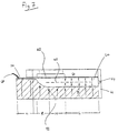
- Figure 7 is sectional view taken along the longitudinal channel axis (indicated by dashed line 65) of a printhead incorporating a channelled piezoelectric component 10 poled in accordance with the present invention.
- a cover member 60 having an ink supply aperture 62 is attached to the tops of the walls 24, thereby closing the channel on all sides parallel to the longitudinal channel axis over a so-called “active" length, denoted L.
- a nozzle 64 formed in a nozzle plate 66 is attached at one end of the channel, whilst at the other end, denoted C, a connection is made (e.g. by wire bond 68) from the channel electrode 30 to drive circuitry (not shown).
- a low dielectric coating is applied to the channel walls prior to any plating so as to reduce the capacitance of the printhead overall.
- WO97/39897 Such an arrangement is known from WO97/39897.
- any conducting layer subsequently deposited in accordance with the present invention is unable to effect either repolarisation or actuation in these areas of the channel.
- Alternative capacitance-reducing measures suitable for use in the non-active areas of the channel include the use of a low-dielectric material to form the channel walls, as described in US 5 619 235, and the reduction the area of the channel electrode to the minimum necessary for conduction of electrical signals from the drive circuit connection 68 at the rear of the printhead (region C) to the full-depth channel electrodes in the active length L of the channel, described in the aforementioned WO97/39897.
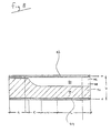
- Figure 8 illustrates an arrangement for repolarising a channelled piezoelectric component of the kind shown in figure 7. Despite the fact that repolarisation is only required in the active portion of the channel, best repolarisation results have been obtained using upper and lower conductive members 42,44 that extend the length of the printhead (and the length of the sheet in the case, described in WO95/18717, where several channelled components are formed in a single sheet).
- a droplet fluid channel may have an active length (L) of around 1mm, a total channel length (L+N+R) of 8.5 mm, a channel width of 75 ⁇ m, a channel wall width of 65 ⁇ m and a channel wall height of 300 ⁇ m.
- a potential difference V of approximately 1000V has been found necessary to reverse the direction of polarisation in the lower wall portion 48 of such a printhead when made from a pre-polarised piezoelectric material such as HD3203 from Motorola.
- an electric field strength of at least 1.2V/ ⁇ m is required before the direction of pre-polarisation starts to change (so-called coercive field strength), with a field of around 1.7V/ ⁇ m being required to achieve permanent repolarisation (so-called field for reversal to saturation) at a level approximately 90% of the initial level of pre-polarisation.
- the corresponding electric field strength in the base portion 50 (which, at around 600 ⁇ m, has a thickness equal to twice the channel height) is of the order of 0.75 V/ ⁇ m and is consequently insufficient to effect permanent repolarisation.
- Figures 9 and 10 illustrate - in sectional views taken parallel and normal to the channel axis respectively - an alternative arrangement for polarising a portion of a piezoelectric actuating wall.
- an electrode 70 is located so as to partially enclose on both sides the lower wall portion 48 lying adjacent the channel bottom surface 26. This may be difficult to manufacture with the conventional 'shaded plating' electrode deposition methods referred to above, although it may be possible to deposit electrode material along the wall surfaces of both upper and lower wall portions 46,48 by such a method and thereafter remove the coating on surface of the upper wall portion 46 by laser, sand blast or similar method.
- a preferred method in accordance with the present invention is to apply an initial, thin 'seed' layer of conducting material to all the channel surfaces, to subsequently remove the seed layer - e.g. by means of a laser or sand blasting - from those areas of the channel walls where an electrode is not required and lastly to employ an electroless plating technique to deposit a thicker layer of electrode material in those areas where the seed layer remains.
- a material for the seed layer is chosen so as to give good adherence to the piezoelectric material and to be deposited in a manner e.g. sputtering, that allows the entire surface of each channel to be coated.
- the seed material chosen is the same as that used for the electrodes themselves, namely aluminium.
- polarising voltage V is subsequently applied between electrode 70 and conductive members 74,76 located on the uppermost surface 72 of the channel wall and the lower surface 40 of the base portion 50 respectively.
- a reversal in polarisation direction results at 78 and 80 whilst that lower portion of the wall 48 enclosed by electrodes 70 remains unaffected.
- a final step of depositing an electrode over the whole depth of each channel wall then allows the actuator walls to be operated in chevron mode.
- the present invention is particularly suited for use with channelled piezoelectric sheets that have been formed by moulding, as generally known e.g. from EP-A-0 600 748.
- a component unlike the commercially available pre-polarised sheet material referred to above, such a component requires polarisation in a single direction throughout its thickness and the application of a masking layer to the tops of the walls prior to application of the techniques outlined above.
- channels may be formed in more than one side of a sheet of piezo-material
- active droplet-ejecting channels may be alternated in the sheet with inactive (so-called “dummy") channels and the nozzle for droplet ejection, rather than being located at the end of the channel, may be arranged intermediate the ends of the channel (the so-called "side-shooter” configuration).
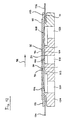
- Figure 12 is a sectional view taken parallel to the channel axis of a such a "side-shooter" printhead incorporating two rows of nozzles 90 and 92 formed in a nozzle plate 93.
- Such an arrangement is notable for the fact that the two rows of nozzles are supplied with ink via respective rows of apertures 94,96 formed in the base of a single channel 20.
- the array of parallel channels is formed in piezoelectric sheet 10 by sawing, the angle of the longitudinal channel axes relative to the direction of motion of the substrate relative to the printhead (denoted by arrow 98) being chosen such that droplets ejected from first row of nozzles 90 are interleaved on the substrate with droplets ejected from the second row of nozzles 92, thereby doubling the print resolution as is known in the art.
- the two nozzles in any given channel will also be offset in the substrate motion direction 98 relative to the two nozzles in the channels lying either side the given channel so as to compensate for the time delays in droplet ejection brought about by the three-cycle firing routine commonly used in "shared wall" printheads.
- Such a routine and associated nozzle offset is well-known, e.g. from EP-A-0 376 532, and consequently will not be discussed in any greater detail here.
- each channel half runs up the respective channel run-out 106, 108 to sheet edges 110,112 where it connects to driver circuitry 114,116 typically in the form of an integrated circuit (IC).
- IC integrated circuit
- Such an IC will normally incorporate drivers for a number (e.g. 66) of adjacent channels and may be connected to ICs driving other groups of channels in the printhead (8 ICs will be required in a printhead having 500 channels) to allow data to be cascaded through as known in the art.
- a particular advantage of the kind of printhead described above is its ability to operate in "multipulse greyscale” mode. As described, e.g. in EP-A-0 422 870, this involves firing a variable number of ink droplets (referred to as a "packet") from a single channel within a short period of time so as to merge in flight and/or on the substrate to form a correspondingly variable-size printed dot. It will appreciated that the use of variable-size printed dots allows a significant increase in image quality over printing with fixed dot size (so-called "binary" printing).
- the disadvantage of such an approach is the concomitant increase in the amount of data to be fed to the driver circuitry for each channel. For example, instructing the ejection of up to fifteen droplets per packet necessary to print photographic quality images with a printhead having a 360 dots-per-inch nozzle pitch requires 16 data levels (15 dot sizes plus zero) expressed in four bits. Measures therefore need to be implemented to ensure sufficient data flow, particularly where there are a large number of nozzles (there may be over 4600 in a 360 dpi printhead having a 12 inch print width) or where the rate at which droplet packets are ejected is high (typically 10 kHz). Such measures, well-known in the art, may include a reduction in the number of ICs that are cascaded together and an associated increase in the number of data inputs necessary to drive each group of cascaded ICs.
- Each of the droplets in a multipulse "packet" will understandably require only a fraction of the volume of a corresponding single droplet ejected by a "binary" printhead. This can be achieved by a combination of reduced active channel length and smaller diameter nozzles - as is known in the art - the increased risk of blockage of the smaller nozzles being offset in the printhead of figure 12 by an arrangement of inlet manifold 118 and outlet manifolds 120, 122 formed in a support 124 that ensures a constant flow of ink past the nozzle, as is well-known per se.
- the present invention is not restricted to the "chevron" polarisation configuration and that there may be instances in which it is desirable to start from a sheet of piezo-material which has not been poled or poled in a direction other than the thickness direction, in which case application of the present invention will result in an upper wall portion that is similarly unpolarised or poled in a direction other than the thickness direction.
Abstract
Description
- The present invention relates to droplet deposition apparatus, particularly inkjet printheads, incorporating piezoelectric actuator elements having first and second portions both deflectable simultaneously to effect ejection of a droplet.
- Such printheads are known, for example, from EP-A-0-277 703 an ink chamber is bounded on at least one side by an actuator wall constructed from upper and lower portions of piezoelectric material bonded together at their common surface and polarised in the plane of the actuator wall in respective opposite senses. When subjected to an electric field perpendicular to the direction of polarisation by electrodes located on opposite sides of the actuator wall, both upper and lower portions deform in shear towards the ink chamber, thereby causing the ejection of a droplet from the ink chamber via a nozzle. Such an actuator wall construction has acquired the name of "chevron" from the shape taken up by the actuator wall as a whole when subject to actuating electric fields.
- JP 01-232812 is concerned with the manufacture of a wafer of lithium tantalate with a first, polarised layer and a second, polarity reversed layer. One side of the wafer is coated with a metal to be diffused in to the wafer, the wafer heated to form a metal diffusion layer in the wafer, the wafer re-polarised to form the first polarised layer and the wafer re-heated at a temperature near the Curie point to form the second, polarity reversed layer.
- To date the techniques for manufacturing chevron printheads have been complex, involving either special piezoelectric laminates into which full-depth ink channels are formed (for example WO92/09436) or the intricate alignment of two piezoelectric sheets each formed with half-depth ink channels (for example the aforementioned EP-A-0 277 703). The actuator walls of such known chevron printheads furthermore include discontinuities in the form of adhesive bonds and/or negative temperature coefficient layers.
- It is an object of the present invention to avoid the complexities of manufacture and structural discontinuities of known chevron constructions.
- Accordingly, the present invention consists in a method of polarising a portion of a monolithic piezoelectric actuator element for use in droplet deposition apparatus, the element having first and second portions, the method comprising the steps of:
- placing a first conducting layer in contact with the first portion of the element and placing the first portion of the element at an equipotential, and
- generating a polarising electric field across the second portion between said first portion and a further conducting layer.
-
- Such a method allows a portion of monolithic piezoelectric element to be subjected to polarising electric fields whilst maintaining another portion of the same element free from repolarisation by holding that portion at an equipotential, advantageously by partial enclosure by a conducting layer which effectively holding that portion free from electric fields in the manner of an at least partial Faraday cage. In the particular case of an actuator element that is initially polarised entirely in one direction, it allows a portion of that element to be repolarised in an opposite direction, the resulting actuator having a chevron poling pattern. The monolithic - i.e. one-piece, integral, homogeneous, uniform - construction of such an actuator avoids the disadvantages of the known constructions discussed above.
- A corresponding component for use in droplet deposition apparatus is included in another aspect of the invention and comprises a homogeneous sheet of piezo-material formed with a multiplicity of parallel, open-topped channels mutually spaced in an array direction normal to the length of the channels and defined each by facing side walls and a bottom surface extending between the side walls;
at least one of said side walls having a first portion remote from a respective bottom surface and a second portion adjacent said respective bottom surface, said second portion being polarised in a direction normal to both the length of the channels and the array direction and said first portion being either unpolarised or polarised in a direction other than said first direction. - Such a component has side walls polarised according to two different regimes and yet retains a homogeneous structure with the associated strength and ease of manufacture that this implies.
- Further advantageous embodiments of the invention are set out in the description and dependent claims.
- The invention is now described by way of example by reference to the following diagrams, of which:
- Figures 1-3 are cross-sectional views taken normal to an ink channel axis illustrating the conventional manufacturing steps involved in the realisation of a first embodiment of the present invention;
- Figures 4 and 5 are cross-sectional views illustrating the application of polarising electric fields in accordance with the present invention;
- Figure 6(a) illustrates the finished actuator with actuating electrodes;
- Figure 6(b) illustrates the displacement of an actuated channel wall;
- Figures 7 and 8 are sectional views along the ink channel axis of a printhead polarised in accordance with a second embodiment of the invention;
- Figures 9-11 are sectional views illustrating the polarisation of a printhead according to a third embodiment of the invention;
- Figure 12 is a sectional view of a further printhead arrangement incorporating the present invention.
-
- Figure 1 is a cross-sectional view of the starting point for the method according to the present invention, namely a monolithic, homogeneous,
uniform sheet 10 of piezo-material (e.g. lead zirconium titanate, PZT) poled in its thickness direction as indicated byarrows 12 and carrying athin layer 14 of masking material on onesurface 16. - Referring to the cross-sectional view of figure 2, a multiplicity of open-
topped channels 20 are formed in thesurface 16 of thesheet 10, thereby to definehomogeneous channel walls 24 of piezo-material, facingside wall surfaces 25 and abottom surface 26 extending between the side wall surfaces. The resultant array of parallel channels extends in a direction lying normal to the longitudinal axes of the channels. - Each
wall 24 then has an electrode 30 - typically of aluminium, nickel or gold - formed on anupper portion 46 thereof, as shown in figure 3, so as to extend in an electrically-continuous fashion approximately half way downwall sides 25 and overmasking layer 16, thereby surrounding theupper portion 46 of each wall. Electrode 30 will also be deposited over maskingmaterial 14 on thesurface 16 of thepiezoelectric sheet 10 in those areas where channels have not been formed. All aspects of the arrangement described above are known in the art, for example from EP-A-0 364 136, EP-A-0 309 148 and EP-A-0 397 441. - Considering now figure 4, a potential difference V is applied between each
electrode 30 and thesurface 40 on the opposite side ofsheet 10 tosurface 16, thereby generating an electric field that is of opposite sign to the initialsheet polarisation direction 12, parallel to theside wall surfaces 25 and perpendicular to the longitudinal axis of the channel (which extends out of the page in the view of figure 4). In the embodiment shown, this is achieved by means of an upperconductive member 42 placed across theelectrodes 30 and by a lowerconductive member 44 pressed againstlower surface 40.Member 44 may itself be a conductive coating, applied to the sheet before formation of the channels or in the course of the deposition of theelectrodes 30. Alternatively, bothmembers conductive member 42, the poling potential difference V can be applied to theelectrode material 30 on the aforementioned area of the sheet surface in which no channels are formed (and which will be in electrical contact with theelectrodes 30 formed on the upper portions of the channel walls). - The strength of the electric field varies throughout the section: in the
upper wall portion 46 remote from thechannel bottom surface 26 and partially enclosed byelectrode 30, no significant electric field is generated as a result of the entirety of theelectrode 30 covering the wall - and consequently theupper wall portion 46 itself - being at an equipotential.Electrode 30 can also be considered as a partial Faraday cage, protecting theupper wall portion 46 which it surrounds from electric fields. As a result, the state of polarisation of the upper wall portion does not change from that of the original sheet (indicated by arrow 12). Althoughelectrode 30 is shown extending over themasking layer 16 located on top of eachchannel wall 24, it will be appreciated that a similar effect will be achieved if theupper wall portion 46 is enclosed by an electrode located only on thechannel wall sides 25, effectively sandwiching the piezoelectric material. - Turning now to the
lower wall portion 48 lying adjacent to thechannel bottom surface 26, there is set up between the lower extremities of theelectrode 30 and thelower surface 40 of thesheet 10 an electric field. Between thelower wall portion 48 and abase portion 50 lying betweenchannel bottom surface 26 and sheetlower surface 40 there is a significant difference is geometry which in turn gives rise to a significantly greater field strength Ew in thelower wall portion 48 compared to the strength Eb in the base portion. - By suitable choice of the value of the potential difference V, a value of field strength Ew can be established in the
lower wall portion 48 that is sufficient to change the direction of polarisation of the piezoelectric material in that portion to a direction - indicated byarrow 52 in figure 4 - opposite to thedirection 12 in which theupper wall portion 46 is polarised, thereby achieving a monolithic wall structure of homogenous, uniform piezo-material that is furthermore polarised in a "chevron" configuration. - The field strength Eb generated in the
base portion 50 will, however, be low enough (approximately 0.5 Ew in the case where channels and channel walls have the same width) not to reverse the direction ofpolarisation 12 of the piezoelectric material in the base. This is in itself advantageous: as explained in the aforementioned EP-A-0 364 136, in an actuator in which the base portion and adjacent wall are polarised in the same direction, fringe electric fields can give rise to a distortion of the base that acts against the motion of the walls, thereby reducing the pressure generated in the ink channel and the velocity of ejection of the ink droplet. In contrast, a base portion that is polarised in the opposite direction to the lower wall portion per figure 4 will tend to act in such a way as to reinforce the pressure generated by the movements of the walls. - It is nevertheless possible to reverse the direction of polarisation of the
base portion 50 by choosing potential difference V to be of sufficient magnitude that not only Ew but also Eb is strong enough to cause a reversal in the direction of polarisation of the wall and base portions of the sheet respectively. - Alternatively, the base portion of the sheet can be repolarised using the arrangement of figure 5 in which
electrodes 30 are extended - for example using the same 'shaded plating' process used in their initial deposition - down to thebottom surface 26 of the channel so as to enclose both upper andlower wall portions bottom surface 26 of the channel as well. A potential difference of sufficient strength to polarise the base in the desired direction, parallel to the direction of polarisation of the upper andlower wall portions lower surface 40 of thesheet 10 so as to generate an electric field sufficient to pole the base portion in the requireddirection 54. Extended electrode 30' again ensures that no repolarisation takes place of those upper andlower wall portions original direction 12 any part of the base that may have lost its polarisation in the course of earlier processing steps. - It will be appreciated that electrodes that extend over the side wall surfaces of both upper and lower wall portions will be required for actuation of the actuator wall, regardless of whether the same electrodes are also used in any repolarisation step. To do this, however, electrodes in adjacent channels must first be electrically isolated from one another. In a final step that is common to both the embodiments of both figures 4 and 5, this is achieved by removing the
masking layer 16 from the top of the channel walls - for example by means of a solvent as is known in the art - the masking layer taking with it any electrode material deposited thereon so as to leave the tops of the walls free and the electrodes in adjacent channels electrically isolated from one another as shown in figure 6(a). Should a conductive coating have been applied to thelower surface 40 of thesheet 10 for poling purposes, this can also be removed if necessary. - The electrodes for each channel can then be connected to respective drive circuitry as is well-known, e.g. from WO95/07820. Figure 6(b) shows, exaggerated, the deflection of a channel wall that results when respective positive and negative voltages (shown schematically but in fact applied via connections at the end of each channel as explained with reference to figure 7) are applied to the electrodes 30' of the
channels 20 either side of the wall. The resulting electric field, oriented normal to the direction of polarisation of the upper andlower wall portions - Figure 7 is sectional view taken along the longitudinal channel axis (indicated by dashed line 65) of a printhead incorporating a channelled
piezoelectric component 10 poled in accordance with the present invention. As is known in the art, a cover member 60 having anink supply aperture 62 is attached to the tops of thewalls 24, thereby closing the channel on all sides parallel to the longitudinal channel axis over a so-called "active" length, denoted L. Anozzle 64 formed in anozzle plate 66 is attached at one end of the channel, whilst at the other end, denoted C, a connection is made (e.g. by wire bond 68) from thechannel electrode 30 to drive circuitry (not shown). - In those "non-active" areas of the channel (R and N) open on at least one side for communication with the
ink supply aperture 62, a low dielectric coating is applied to the channel walls prior to any plating so as to reduce the capacitance of the printhead overall. Such an arrangement is known from WO97/39897. As a result, any conducting layer subsequently deposited in accordance with the present invention is unable to effect either repolarisation or actuation in these areas of the channel. - Alternative capacitance-reducing measures suitable for use in the non-active areas of the channel include the use of a low-dielectric material to form the channel walls, as described in
US 5 619 235, and the reduction the area of the channel electrode to the minimum necessary for conduction of electrical signals from the drive circuit connection 68 at the rear of the printhead (region C) to the full-depth channel electrodes in the active length L of the channel, described in the aforementioned WO97/39897. - Figure 8 illustrates an arrangement for repolarising a channelled piezoelectric component of the kind shown in figure 7. Despite the fact that repolarisation is only required in the active portion of the channel, best repolarisation results have been obtained using upper and lower
conductive members - In a typical printhead, a droplet fluid channel may have an active length (L) of around 1mm, a total channel length (L+N+R) of 8.5 mm, a channel width of 75µm, a channel wall width of 65µm and a channel wall height of 300µm. A potential difference V of approximately 1000V has been found necessary to reverse the direction of polarisation in the
lower wall portion 48 of such a printhead when made from a pre-polarised piezoelectric material such as HD3203 from Motorola. It has been established that in such material, an electric field strength of at least 1.2V/µm is required before the direction of pre-polarisation starts to change (so-called coercive field strength), with a field of around 1.7V/µm being required to achieve permanent repolarisation (so-called field for reversal to saturation) at a level approximately 90% of the initial level of pre-polarisation. The corresponding electric field strength in the base portion 50 (which, at around 600µm, has a thickness equal to twice the channel height) is of the order of 0.75 V/µm and is consequently insufficient to effect permanent repolarisation. - It will be appreciated that the high value of poling voltage V applied across the relatively low thickness of the channelled
piezoelectric sheet 10 necessitates the use of a non-conducting atmosphere to avoid arcing. Fluorinert (a Trade Mark of DuPont) has been found to be particularly effective in this regard, although it is noted that polarisation under a vacuum could conveniently be carried out in the same chamber as any preceding or subsequent electrode deposition steps, reducing manufacturing time. - Figures 9 and 10 illustrate - in sectional views taken parallel and normal to the channel axis respectively - an alternative arrangement for polarising a portion of a piezoelectric actuating wall. In contrast to the arrangement of figure 4, an
electrode 70 is located so as to partially enclose on both sides thelower wall portion 48 lying adjacent thechannel bottom surface 26. This may be difficult to manufacture with the conventional 'shaded plating' electrode deposition methods referred to above, although it may be possible to deposit electrode material along the wall surfaces of both upper andlower wall portions upper wall portion 46 by laser, sand blast or similar method. - A preferred method in accordance with the present invention is to apply an initial, thin 'seed' layer of conducting material to all the channel surfaces, to subsequently remove the seed layer - e.g. by means of a laser or sand blasting - from those areas of the channel walls where an electrode is not required and lastly to employ an electroless plating technique to deposit a thicker layer of electrode material in those areas where the seed layer remains. A material for the seed layer is chosen so as to give good adherence to the piezoelectric material and to be deposited in a manner e.g. sputtering, that allows the entire surface of each channel to be coated. In the present example, the seed material chosen is the same as that used for the electrodes themselves, namely aluminium.
- As illustrated in figure 11, polarising voltage V is subsequently applied between
electrode 70 andconductive members uppermost surface 72 of the channel wall and thelower surface 40 of thebase portion 50 respectively. A reversal in polarisation direction results at 78 and 80 whilst that lower portion of thewall 48 enclosed byelectrodes 70 remains unaffected. It will be appreciated that the arrangement of figure 11, withelectrode 70 positioned in the middle of the sheet rather that on the upper surface as is the case withelectrode 30 of figure 4, allows greater repolarisation field densities both in theupper wall 46 portion remote from the channel bottom surface and in the base 50 portion. This is turn allows a reduced polarisation voltage to be employed, with the attendant advantages in terms of size of voltage supply required, the necessary anti-arcing measures, etc. - A final step of depositing an electrode over the whole depth of each channel wall then allows the actuator walls to be operated in chevron mode.
- The present invention is particularly suited for use with channelled piezoelectric sheets that have been formed by moulding, as generally known e.g. from EP-A-0 600 748. However, unlike the commercially available pre-polarised sheet material referred to above, such a component requires polarisation in a single direction throughout its thickness and the application of a masking layer to the tops of the walls prior to application of the techniques outlined above.
- It will be appreciated that the present invention has been described by way of examples only and that a wide variety of modifications can be made without departing from the scope of the invention. For example, channels may be formed in more than one side of a sheet of piezo-material, active droplet-ejecting channels may be alternated in the sheet with inactive (so-called "dummy") channels and the nozzle for droplet ejection, rather than being located at the end of the channel, may be arranged intermediate the ends of the channel (the so-called "side-shooter" configuration).
- Figure 12 is a sectional view taken parallel to the channel axis of a such a "side-shooter" printhead incorporating two rows of
nozzles 90 and 92 formed in anozzle plate 93. Such an arrangement is notable for the fact that the two rows of nozzles are supplied with ink via respective rows ofapertures single channel 20. In the example shown, the array of parallel channels is formed inpiezoelectric sheet 10 by sawing, the angle of the longitudinal channel axes relative to the direction of motion of the substrate relative to the printhead (denoted by arrow 98) being chosen such that droplets ejected from first row of nozzles 90 are interleaved on the substrate with droplets ejected from the second row ofnozzles 92, thereby doubling the print resolution as is known in the art. The two nozzles in any given channel will also be offset in thesubstrate motion direction 98 relative to the two nozzles in the channels lying either side the given channel so as to compensate for the time delays in droplet ejection brought about by the three-cycle firing routine commonly used in "shared wall" printheads. Such a routine and associated nozzle offset is well-known, e.g. from EP-A-0 376 532, and consequently will not be discussed in any greater detail here. - With the exception of
break 100 separating the electrodes in thathalf 102 of the channel supplying nozzle 90 from thathalf 104 supplyingnozzle 92, thereby allowing independent operation of the two channel halves, the construction of the channel of figure 12 is the same as described previously. The electrode in each channel half runs up the respective channel run-out 106, 108 to sheet edges 110,112 where it connects to driver circuitry 114,116 typically in the form of an integrated circuit (IC). Such an IC will normally incorporate drivers for a number (e.g. 66) of adjacent channels and may be connected to ICs driving other groups of channels in the printhead (8 ICs will be required in a printhead having 500 channels) to allow data to be cascaded through as known in the art. - A particular advantage of the kind of printhead described above is its ability to operate in "multipulse greyscale" mode. As described, e.g. in EP-A-0 422 870, this involves firing a variable number of ink droplets (referred to as a "packet") from a single channel within a short period of time so as to merge in flight and/or on the substrate to form a correspondingly variable-size printed dot. It will appreciated that the use of variable-size printed dots allows a significant increase in image quality over printing with fixed dot size (so-called "binary" printing).
- The disadvantage of such an approach is the concomitant increase in the amount of data to be fed to the driver circuitry for each channel. For example, instructing the ejection of up to fifteen droplets per packet necessary to print photographic quality images with a printhead having a 360 dots-per-inch nozzle pitch requires 16 data levels (15 dot sizes plus zero) expressed in four bits. Measures therefore need to be implemented to ensure sufficient data flow, particularly where there are a large number of nozzles (there may be over 4600 in a 360 dpi printhead having a 12 inch print width) or where the rate at which droplet packets are ejected is high (typically 10 kHz). Such measures, well-known in the art, may include a reduction in the number of ICs that are cascaded together and an associated increase in the number of data inputs necessary to drive each group of cascaded ICs.
- Each of the droplets in a multipulse "packet" will understandably require only a fraction of the volume of a corresponding single droplet ejected by a "binary" printhead. This can be achieved by a combination of reduced active channel length and smaller diameter nozzles - as is known in the art - the increased risk of blockage of the smaller nozzles being offset in the printhead of figure 12 by an arrangement of
inlet manifold 118 and outlet manifolds 120, 122 formed in asupport 124 that ensures a constant flow of ink past the nozzle, as is well-known per se. - The present invention is not restricted to the "chevron" polarisation configuration and that there may be instances in which it is desirable to start from a sheet of piezo-material which has not been poled or poled in a direction other than the thickness direction, in which case application of the present invention will result in an upper wall portion that is similarly unpolarised or poled in a direction other than the thickness direction.
Claims (24)
- Method of polarising a portion of a monolithic piezoelectric actuator element (24) for use in droplet deposition apparatus, the element having first and second portions, the method comprising the steps of:placing a first conducting layer (30) in contact with the first portion (46) of the element and placing the first portion (46) of the element at an equipotential, andgenerating a polarising electric field across the second portion (48) between said first portion (46) and a further conducting layer (44).
- Method according to Claim 1, wherein said step of placing the first portion (46) of the element (24) at an equipotential includes the location of the first conducting layer (30) so as to partially enclose the first portion (46).
- Method according to any previous claim, wherein the first portion (46) of the element (24) is polarised.
- Method according to Claim 3 and further comprising the step of generating a polarising electric field across the second portion (48) in a direction such as to polarise the second portion (48) in a direction opposite to the direction of polarisation of the first portion (46) of the element (24).
- Method according to any previous claim, wherein the first portion (46) of the element is polarised in a direction perpendicular to the direction in which said portions (46, 48) are deflectable to effect ejection of a droplet from said droplet deposition apparatus.
- Method according to any previous claim, wherein the piezoelectric actuator element (24) is defined between two channels formed in a homogeneous sheet (10) of piezo-material, each channel (20) being defined by facing side wall surfaces (25) and a bottom surface (26) extending between the side wall surfaces (25).
- Method according to Claim 6, wherein at least one of the said two channels is adapted to contain droplet fluid.
- Method according to Claim 6 and including the step of generating a polarising electric field in direction parallel to said facing side wall surfaces (25) and perpendicular to the longitudinal axis of the channel (20).
- Method according to any of Claims 6 to 8, wherein said first and second portions (46, 48) lie remote from and adjacent to a respective channel bottom surface (26) respectively.
- Method according to any of Claims 6-8, wherein said first and second portions (46, 48) lie adjacent to and remote from a respective channel bottom surface (26) respectively.
- Method according to any of Claims 6 to 10, wherein at least one of said two channels is formed in a first surface (16) of said sheet (10), a further portion (50) of the sheet (10) lying between the bottom surface (26) of said at least one of the two channels and the opposite surface (40) of the sheet (10) to said first surface (16).
- Method according to Claim 11, wherein said further portion (50) is polarised in a direction parallel to the direction of polarisation of said first portion (46).
- Method according to Claim 11 and further comprising the steps of locating a second conducting layer (30) so as to partially enclose said first and second potions (46, 48) and generating a polarising electric field across the further portion (50) between the second conducting layer (30) and said further conducting layer (44).
- Method according to any previous claim and further comprising the step of locating actuating electrodes (30) on said first and second portions (46, 48) so as to be able to deflect both portions simultaneously.
- Method according to Claim 14 and further comprising the step of locating said actuating electrodes (30) so as to apply an electric field in a direction normal to the direction of polarisation of said second portion (48).
- Method according to Claim 15 when dependent on any of Claims 6 to 13 and further comprising the step of locating said actuating electrodes (30) on respective facing side wall surfaces (25).
- Component for use in droplet deposition apparatus comprising:a homogeneous sheet (10) of piezo-material formed with a multiplicity of parallel, open-topped channels (20) mutually spaced in an array direction normal to the length of the channels and defined each by facing side walls (24) and a bottom surface (26) extending between the side walls (24);at least one of said side walls (24) having a first portion (46) remote from a respective bottom surface (26) and a second portion (48) adjacent said respective bottom surface (26), said second portion (48) being polarised in a direction normal to both the length of the channels and the array direction and said first portion (46) being either unpolarised or polarised in a direction other than said first direction.
- Component according to Claim 17, wherein said first and second portions (46, 48) are polarised in opposite directions that lie normal to both the length of the channels (20) and to the array direction.
- Component according to Claim 17 or 18, wherein at least one of said two channels is formed in a first surface(16) of said sheet (10), a further portion (50) of the sheet(10) lying between the bottom surface (26) of said at least one of the two channels and the opposite surface (40) of the sheet (10) to said first surface (16).
- Component according to Claim 19, wherein said further portion (50) is polarised in a direction parallel to the direction of polarisation of said first portion (46).
- Component according to Claim 20, wherein said further portion (50) is polarised in a direction opposite to that of said first portion (46).
- Component according to any of Claims 17 to 21, wherein actuating electrodes (30) are located on said first and second portions (46, 48) so as to be able to deflect both portions simultaneously.
- Component according to Claim 22, wherein said actuating electrodes (30) are located so as to apply an electric field in a direction perpendicular to the direction of polarisation of said second portion (48).
- Component according to Claims 22 or 23, wherein said actuating electrodes (30) are located on respective facing side walls (24).
Applications Claiming Priority (3)
| Application Number | Priority Date | Filing Date | Title |
|---|---|---|---|
| GBGB9805038.8A GB9805038D0 (en) | 1998-03-11 | 1998-03-11 | Droplet deposition apparatus and method of manufacture |
| GB9805038 | 1998-03-11 | ||
| PCT/GB1999/000718 WO1999046127A1 (en) | 1998-03-11 | 1999-03-10 | Droplet deposition apparatus and method of manufacture |
Publications (2)
| Publication Number | Publication Date |
|---|---|
| EP1062098A1 EP1062098A1 (en) | 2000-12-27 |
| EP1062098B1 true EP1062098B1 (en) | 2002-06-05 |
Family
ID=10828275
Family Applications (1)
| Application Number | Title | Priority Date | Filing Date |
|---|---|---|---|
| EP99907758A Expired - Lifetime EP1062098B1 (en) | 1998-03-11 | 1999-03-10 | Droplet deposition apparatus and method of manufacture |
Country Status (13)
| Country | Link |
|---|---|
| US (1) | US6505918B1 (en) |
| EP (1) | EP1062098B1 (en) |
| JP (1) | JP3694652B2 (en) |
| CN (1) | CN1158181C (en) |
| AT (1) | ATE218443T1 (en) |
| AU (1) | AU2738899A (en) |
| BR (1) | BR9908633A (en) |
| CA (1) | CA2324290A1 (en) |
| DE (1) | DE69901691T2 (en) |
| ES (1) | ES2174593T3 (en) |
| GB (1) | GB9805038D0 (en) |
| IL (1) | IL138370A0 (en) |
| WO (1) | WO1999046127A1 (en) |
Families Citing this family (15)
| Publication number | Priority date | Publication date | Assignee | Title |
|---|---|---|---|---|
| GB0000368D0 (en) * | 2000-01-07 | 2000-03-01 | Xaar Technology Ltd | Droplet deposition apparatus |
| US8251471B2 (en) * | 2003-08-18 | 2012-08-28 | Fujifilm Dimatix, Inc. | Individual jet voltage trimming circuitry |
| US8085428B2 (en) | 2004-10-15 | 2011-12-27 | Fujifilm Dimatix, Inc. | Print systems and techniques |
| US7907298B2 (en) * | 2004-10-15 | 2011-03-15 | Fujifilm Dimatix, Inc. | Data pump for printing |
| US7722147B2 (en) * | 2004-10-15 | 2010-05-25 | Fujifilm Dimatix, Inc. | Printing system architecture |
| US8068245B2 (en) * | 2004-10-15 | 2011-11-29 | Fujifilm Dimatix, Inc. | Printing device communication protocol |
| US7911625B2 (en) * | 2004-10-15 | 2011-03-22 | Fujifilm Dimatrix, Inc. | Printing system software architecture |
| US8199342B2 (en) * | 2004-10-29 | 2012-06-12 | Fujifilm Dimatix, Inc. | Tailoring image data packets to properties of print heads |
| US7234788B2 (en) * | 2004-11-03 | 2007-06-26 | Dimatix, Inc. | Individual voltage trimming with waveforms |
| US7556327B2 (en) * | 2004-11-05 | 2009-07-07 | Fujifilm Dimatix, Inc. | Charge leakage prevention for inkjet printing |
| US8182068B2 (en) * | 2009-07-29 | 2012-05-22 | Eastman Kodak Company | Printhead including dual nozzle structure |
| JP5633200B2 (en) * | 2010-06-08 | 2014-12-03 | 株式会社リコー | Piezoelectric actuator, liquid discharge head, and image forming apparatus |
| TWI511886B (en) * | 2011-11-18 | 2015-12-11 | Canon Kk | Liquid discharging device |
| JP2015168177A (en) | 2014-03-07 | 2015-09-28 | エスアイアイ・プリンテック株式会社 | Liquid injection head and liquid injection device |
| CN111403595B (en) * | 2020-04-14 | 2023-09-26 | 北京汽车集团越野车有限公司 | Preparation method of piezoelectric ceramic multi-actuation wall structure |
Family Cites Families (11)
| Publication number | Priority date | Publication date | Assignee | Title |
|---|---|---|---|---|
| JPS59117814A (en) * | 1982-12-24 | 1984-07-07 | Murata Mfg Co Ltd | Piezoelectric porcelain resonator |
| US4633204A (en) | 1984-08-29 | 1986-12-30 | Fujitsu Limited | Mechanical filter |
| JPS6157108A (en) * | 1984-08-29 | 1986-03-24 | Fujitsu Ltd | Piezoelectric ceramic vibrator |
| US4887100A (en) * | 1987-01-10 | 1989-12-12 | Am International, Inc. | Droplet deposition apparatus |
| JPH01232811A (en) * | 1988-03-12 | 1989-09-18 | Fujitsu Ltd | Manufacture of piezoelectric vibrator |
| JPH01232812A (en) * | 1988-03-14 | 1989-09-18 | Fujitsu Ltd | Method for forming lithium tantalate wafer polarized inverting layer |
| JP3087315B2 (en) * | 1991-02-13 | 2000-09-11 | セイコーエプソン株式会社 | Ink jet head and method of manufacturing the same |
| JP2749475B2 (en) * | 1991-10-04 | 1998-05-13 | 株式会社テック | Method of manufacturing ink jet printer head |
| JP3189491B2 (en) * | 1993-05-26 | 2001-07-16 | ブラザー工業株式会社 | Ink jet device |
| GB9318985D0 (en) * | 1993-09-14 | 1993-10-27 | Xaar Ltd | Passivation of ceramic piezoelectric ink jet print heads |
| EP0693789A3 (en) * | 1994-07-18 | 1996-05-29 | Tokin Corp | Piezoelectric transformer with primary and secondary electrodes isolated from each other and voltage converter using the same |
-
1998
- 1998-03-11 GB GBGB9805038.8A patent/GB9805038D0/en not_active Ceased
-
1999
- 1999-03-10 BR BR9908633-6A patent/BR9908633A/en active Search and Examination
- 1999-03-10 EP EP99907758A patent/EP1062098B1/en not_active Expired - Lifetime
- 1999-03-10 CA CA002324290A patent/CA2324290A1/en not_active Abandoned
- 1999-03-10 AU AU27388/99A patent/AU2738899A/en not_active Abandoned
- 1999-03-10 AT AT99907758T patent/ATE218443T1/en not_active IP Right Cessation
- 1999-03-10 WO PCT/GB1999/000718 patent/WO1999046127A1/en active IP Right Grant
- 1999-03-10 IL IL13837099A patent/IL138370A0/en not_active IP Right Cessation
- 1999-03-10 DE DE69901691T patent/DE69901691T2/en not_active Expired - Lifetime
- 1999-03-10 JP JP2000535521A patent/JP3694652B2/en not_active Expired - Fee Related
- 1999-03-10 ES ES99907758T patent/ES2174593T3/en not_active Expired - Lifetime
- 1999-03-10 CN CNB99805674XA patent/CN1158181C/en not_active Expired - Fee Related
-
2000
- 2000-09-08 US US09/657,671 patent/US6505918B1/en not_active Expired - Fee Related
Also Published As
| Publication number | Publication date |
|---|---|
| EP1062098A1 (en) | 2000-12-27 |
| WO1999046127A1 (en) | 1999-09-16 |
| CN1299319A (en) | 2001-06-13 |
| US6505918B1 (en) | 2003-01-14 |
| BR9908633A (en) | 2000-12-12 |
| JP2002505972A (en) | 2002-02-26 |
| AU2738899A (en) | 1999-09-27 |
| CN1158181C (en) | 2004-07-21 |
| JP3694652B2 (en) | 2005-09-14 |
| IL138370A0 (en) | 2001-10-31 |
| CA2324290A1 (en) | 1999-09-16 |
| ATE218443T1 (en) | 2002-06-15 |
| ES2174593T3 (en) | 2002-11-01 |
| DE69901691T2 (en) | 2003-01-09 |
| DE69901691D1 (en) | 2002-07-11 |
| GB9805038D0 (en) | 1998-05-06 |
Similar Documents
| Publication | Publication Date | Title |
|---|---|---|
| EP1062098B1 (en) | Droplet deposition apparatus and method of manufacture | |
| EP0721839B1 (en) | Layered-type piezoelectric element and method for producing the layered-type piezoelectric element | |
| US7159971B2 (en) | Multi-nozzle ink jet head | |
| JP3697829B2 (en) | Inkjet head manufacturing method | |
| EP0511376A4 (en) | Thin-film transducer ink jet head | |
| EP0528649B1 (en) | Method of manufacturing a high density ink jet printhead array | |
| US20030107622A1 (en) | Piezoelectric actuator | |
| JP4829165B2 (en) | Piezoelectric element manufacturing method and liquid discharge head manufacturing method | |
| EP1336495B1 (en) | Ink-jet head and ink-jet printer | |
| EP0695641A2 (en) | Arrangement for plate-like piezoelectric actuators and method of manufacturing | |
| JP2003224312A (en) | Piezoelectric transducer and droplet injection device using it | |
| JPH05301342A (en) | Ink jet printing head | |
| US5945773A (en) | Piezoelectric actuator for ink-jet printer and method of manufacturing the same | |
| EP0658142B1 (en) | Ink jet print head | |
| EP1456034A2 (en) | Low voltage ink jet printing module | |
| JP3214017B2 (en) | Laminated piezoelectric displacement element and ink jet print head | |
| EP1493574B1 (en) | Method for manufacturing inkjet printing head | |
| JP3306937B2 (en) | Inkjet head | |
| JP2001058401A (en) | Ink-jet head | |
| JPH11188865A (en) | Ink jet recording apparatus | |
| JP3506356B2 (en) | Inkjet printer head | |
| JP3024291B2 (en) | Droplet ejector | |
| JP2981499B2 (en) | Inkjet head | |
| JPH09131864A (en) | Ink-jet head | |
| JPH081933A (en) | Piezoelectric vibrator array |
Legal Events
| Date | Code | Title | Description |
|---|---|---|---|
| PUAI | Public reference made under article 153(3) epc to a published international application that has entered the european phase |
Free format text: ORIGINAL CODE: 0009012 |
|
| 17P | Request for examination filed |
Effective date: 20000914 |
|
| AK | Designated contracting states |
Kind code of ref document: A1 Designated state(s): AT CH DE ES FR GB IT LI NL SE |
|
| 17Q | First examination report despatched |
Effective date: 20010212 |
|
| GRAG | Despatch of communication of intention to grant |
Free format text: ORIGINAL CODE: EPIDOS AGRA |
|
| GRAG | Despatch of communication of intention to grant |
Free format text: ORIGINAL CODE: EPIDOS AGRA |
|
| GRAH | Despatch of communication of intention to grant a patent |
Free format text: ORIGINAL CODE: EPIDOS IGRA |
|
| GRAH | Despatch of communication of intention to grant a patent |
Free format text: ORIGINAL CODE: EPIDOS IGRA |
|
| GRAA | (expected) grant |
Free format text: ORIGINAL CODE: 0009210 |
|
| AK | Designated contracting states |
Kind code of ref document: B1 Designated state(s): AT CH DE ES FR GB IT LI NL SE |
|
| REF | Corresponds to: |
Ref document number: 218443 Country of ref document: AT Date of ref document: 20020615 Kind code of ref document: T |
|
| REG | Reference to a national code |
Ref country code: GB Ref legal event code: FG4D |
|
| REG | Reference to a national code |
Ref country code: CH Ref legal event code: EP |
|
| REF | Corresponds to: |
Ref document number: 69901691 Country of ref document: DE Date of ref document: 20020711 |
|
| REG | Reference to a national code |
Ref country code: CH Ref legal event code: NV Representative=s name: ISLER & PEDRAZZINI AG |
|
| ET | Fr: translation filed | ||
| REG | Reference to a national code |
Ref country code: ES Ref legal event code: FG2A Ref document number: 2174593 Country of ref document: ES Kind code of ref document: T3 |
|
| PGFP | Annual fee paid to national office [announced via postgrant information from national office to epo] |
Ref country code: SE Payment date: 20030306 Year of fee payment: 5 |
|
| PGFP | Annual fee paid to national office [announced via postgrant information from national office to epo] |
Ref country code: AT Payment date: 20030312 Year of fee payment: 5 |
|
| PGFP | Annual fee paid to national office [announced via postgrant information from national office to epo] |
Ref country code: CH Payment date: 20030314 Year of fee payment: 5 |
|
| PGFP | Annual fee paid to national office [announced via postgrant information from national office to epo] |
Ref country code: NL Payment date: 20030327 Year of fee payment: 5 |
|
| PLBE | No opposition filed within time limit |
Free format text: ORIGINAL CODE: 0009261 |
|
| STAA | Information on the status of an ep patent application or granted ep patent |
Free format text: STATUS: NO OPPOSITION FILED WITHIN TIME LIMIT |
|
| 26N | No opposition filed |
Effective date: 20030306 |
|
| PG25 | Lapsed in a contracting state [announced via postgrant information from national office to epo] |
Ref country code: AT Free format text: LAPSE BECAUSE OF NON-PAYMENT OF DUE FEES Effective date: 20040310 |
|
| PG25 | Lapsed in a contracting state [announced via postgrant information from national office to epo] |
Ref country code: SE Free format text: LAPSE BECAUSE OF NON-PAYMENT OF DUE FEES Effective date: 20040311 |
|
| PG25 | Lapsed in a contracting state [announced via postgrant information from national office to epo] |
Ref country code: LI Free format text: LAPSE BECAUSE OF NON-PAYMENT OF DUE FEES Effective date: 20040331 Ref country code: CH Free format text: LAPSE BECAUSE OF NON-PAYMENT OF DUE FEES Effective date: 20040331 |
|
| PG25 | Lapsed in a contracting state [announced via postgrant information from national office to epo] |
Ref country code: NL Free format text: LAPSE BECAUSE OF NON-PAYMENT OF DUE FEES Effective date: 20041001 |
|
| EUG | Se: european patent has lapsed | ||
| REG | Reference to a national code |
Ref country code: CH Ref legal event code: PL |
|
| NLV4 | Nl: lapsed or anulled due to non-payment of the annual fee |
Effective date: 20041001 |
|
| PGFP | Annual fee paid to national office [announced via postgrant information from national office to epo] |
Ref country code: IT Payment date: 20080327 Year of fee payment: 10 |
|
| PGFP | Annual fee paid to national office [announced via postgrant information from national office to epo] |
Ref country code: ES Payment date: 20080418 Year of fee payment: 10 |
|
| REG | Reference to a national code |
Ref country code: ES Ref legal event code: FD2A Effective date: 20090311 |
|
| PG25 | Lapsed in a contracting state [announced via postgrant information from national office to epo] |
Ref country code: ES Free format text: LAPSE BECAUSE OF NON-PAYMENT OF DUE FEES Effective date: 20090311 |
|
| PG25 | Lapsed in a contracting state [announced via postgrant information from national office to epo] |
Ref country code: IT Free format text: LAPSE BECAUSE OF NON-PAYMENT OF DUE FEES Effective date: 20090310 |
|
| PGFP | Annual fee paid to national office [announced via postgrant information from national office to epo] |
Ref country code: FR Payment date: 20110317 Year of fee payment: 13 |
|
| PGFP | Annual fee paid to national office [announced via postgrant information from national office to epo] |
Ref country code: GB Payment date: 20110309 Year of fee payment: 13 |
|
| PGFP | Annual fee paid to national office [announced via postgrant information from national office to epo] |
Ref country code: DE Payment date: 20120411 Year of fee payment: 14 |
|
| GBPC | Gb: european patent ceased through non-payment of renewal fee |
Effective date: 20120310 |
|
| REG | Reference to a national code |
Ref country code: FR Ref legal event code: ST Effective date: 20121130 |
|
| PG25 | Lapsed in a contracting state [announced via postgrant information from national office to epo] |
Ref country code: FR Free format text: LAPSE BECAUSE OF NON-PAYMENT OF DUE FEES Effective date: 20120402 Ref country code: GB Free format text: LAPSE BECAUSE OF NON-PAYMENT OF DUE FEES Effective date: 20120310 |
|
| REG | Reference to a national code |
Ref country code: DE Ref legal event code: R119 Ref document number: 69901691 Country of ref document: DE Effective date: 20131001 |
|
| PG25 | Lapsed in a contracting state [announced via postgrant information from national office to epo] |
Ref country code: DE Free format text: LAPSE BECAUSE OF NON-PAYMENT OF DUE FEES Effective date: 20131001 |