EP1061528A1 - Memory testing - Google Patents
Memory testing Download PDFInfo
- Publication number
- EP1061528A1 EP1061528A1 EP00302825A EP00302825A EP1061528A1 EP 1061528 A1 EP1061528 A1 EP 1061528A1 EP 00302825 A EP00302825 A EP 00302825A EP 00302825 A EP00302825 A EP 00302825A EP 1061528 A1 EP1061528 A1 EP 1061528A1
- Authority
- EP
- European Patent Office
- Prior art keywords
- output
- circuitry
- clock
- sense amplifier
- timing signal
- Prior art date
- Legal status (The legal status is an assumption and is not a legal conclusion. Google has not performed a legal analysis and makes no representation as to the accuracy of the status listed.)
- Withdrawn
Links
- 230000015654 memory Effects 0.000 title claims description 41
- 238000012360 testing method Methods 0.000 title claims description 11
- 238000000034 method Methods 0.000 claims abstract description 24
- 230000004044 response Effects 0.000 claims abstract description 4
- 238000012544 monitoring process Methods 0.000 claims description 8
- 230000008878 coupling Effects 0.000 claims description 2
- 238000010168 coupling process Methods 0.000 claims description 2
- 238000005859 coupling reaction Methods 0.000 claims description 2
- 230000000295 complement effect Effects 0.000 description 8
- 238000005259 measurement Methods 0.000 description 4
- 239000011159 matrix material Substances 0.000 description 3
- 239000000872 buffer Substances 0.000 description 2
- 238000010586 diagram Methods 0.000 description 2
- 230000007704 transition Effects 0.000 description 2
- 230000009471 action Effects 0.000 description 1
- 230000008859 change Effects 0.000 description 1
- 230000001934 delay Effects 0.000 description 1
- 230000003111 delayed effect Effects 0.000 description 1
- 238000013101 initial test Methods 0.000 description 1
- 238000004519 manufacturing process Methods 0.000 description 1
- 230000009467 reduction Effects 0.000 description 1
- 230000000630 rising effect Effects 0.000 description 1
- 239000004065 semiconductor Substances 0.000 description 1
Images


Classifications
-
- G—PHYSICS
- G11—INFORMATION STORAGE
- G11C—STATIC STORES
- G11C29/00—Checking stores for correct operation ; Subsequent repair; Testing stores during standby or offline operation
- G11C29/02—Detection or location of defective auxiliary circuits, e.g. defective refresh counters
- G11C29/028—Detection or location of defective auxiliary circuits, e.g. defective refresh counters with adaption or trimming of parameters
-
- G—PHYSICS
- G11—INFORMATION STORAGE
- G11C—STATIC STORES
- G11C29/00—Checking stores for correct operation ; Subsequent repair; Testing stores during standby or offline operation
- G11C29/04—Detection or location of defective memory elements, e.g. cell constructio details, timing of test signals
- G11C29/50—Marginal testing, e.g. race, voltage or current testing
-
- G—PHYSICS
- G11—INFORMATION STORAGE
- G11C—STATIC STORES
- G11C29/00—Checking stores for correct operation ; Subsequent repair; Testing stores during standby or offline operation
- G11C29/04—Detection or location of defective memory elements, e.g. cell constructio details, timing of test signals
- G11C29/50—Marginal testing, e.g. race, voltage or current testing
- G11C29/50012—Marginal testing, e.g. race, voltage or current testing of timing
-
- G—PHYSICS
- G11—INFORMATION STORAGE
- G11C—STATIC STORES
- G11C11/00—Digital stores characterised by the use of particular electric or magnetic storage elements; Storage elements therefor
- G11C11/21—Digital stores characterised by the use of particular electric or magnetic storage elements; Storage elements therefor using electric elements
- G11C11/34—Digital stores characterised by the use of particular electric or magnetic storage elements; Storage elements therefor using electric elements using semiconductor devices
- G11C11/40—Digital stores characterised by the use of particular electric or magnetic storage elements; Storage elements therefor using electric elements using semiconductor devices using transistors
- G11C11/41—Digital stores characterised by the use of particular electric or magnetic storage elements; Storage elements therefor using electric elements using semiconductor devices using transistors forming static cells with positive feedback, i.e. cells not needing refreshing or charge regeneration, e.g. bistable multivibrator or Schmitt trigger
Definitions
- the present invention relates to a method of operating a device such as a memory, a testing device for a memory and to a method of determining a minimum sense amplifier clock delay.
- Semiconductor memories have a matrix of memory cells, the matrix having rows formed by wordlines and columns formed by complementary pairs of bitlines.
- the bitline pairs are connected to clocked sense amplifiers which evaluate the contents of a cell which is connected to the bitlines.
- the complementary bitlines tend to have a high capacitance and the memory cells tend to have a relatively low current driving capability which means that the differential voltage across the complementary pair of bitlines increases relatively slowly.
- sense amplifiers normally have an input offset. This offset, which may be positive or negative, must be overcome by the differential voltage on the bitlines before the sense amplifier can latch into the correct state.
- the present invention aims to provide a technique for determining the minimum sense amplifier clock delay, which minimum delay still gives rise to a correct output from the sense amplifier.
- a method of operating a device comprising circuitry having an input responsive to a first timing signal and producing a valid output to clocked output circuitry after a first delay, said clocked output circuitry having a clock node, and a clock delay circuit responsive to said first timing signal for providing at a second delay, a second timing signal to said clock node of said clocked output circuitry, the method comprising repeatedly applying said first timing signal followed by an external timing signal, wherein said external timing signal is applied via a delay-producing first path to said clock node; monitoring an output of said clocked output circuitry; varying the delay of application of said external timing signal with respect to said first timing signal; and in response to a desired output of said clocked output circuitry, modifying said second delay.
- said desired output is a just valid output such that any reduced delay in said external timing signal gives rise to an invalid output.
- said method further comprises determining when said second timing signal occurs and, during said repeatedly applying step, determining when said desired output occurs.
- said step of determining when said second timing signal occurs comprises providing latch circuitry responsive to the output of said clocked output circuitry, said latch circuitry having a latch clock node connected to a latch clock pad via a delay producing second path; successively providing said second timing signal to said clock node of said clocked output circuitry and a latch timing signal to said latch clock pad; varying the time of occurrence of said latch timing signal; and monitoring the latch circuitry output.
- the method further comprises applying the externally generated clock signal via the delay-producing first path to said clock node and varying the time thereof; and monitoring the latch circuitry output.
- said device is a memory comprising an address register having a clock input, an array of memory cells having wordlines connected to said address register, and plural bitlines and clocked sense amplifiers for evaluating said bitlines.
- a method of determining a minimum sense amplifier clock delay in a memory comprising address register circuitry having a clock input, an array of memory cells having wordlines coupled to said address register circuitry and bitlines connected to sense amplifier circuitry, said sense amplifier circuitry having a clock input, the memory further having output circuitry having an input coupled to the output of said sense amplifier circuitry and an output, the method comprising:-
- said output circuitry has an output circuitry clock input
- said memory further comprises a sense amplifier clock generator having an output
- said method comprises, before said repeatedly applying step, the repeated steps of applying first timing signals at said first path, and applying the output of said sense amplifier clock pulse generator to said clock input of said sense amplifier circuitry whilst varying the delay of application of a timing signal with respect to said first timing signal to said clock input of said output circuitry until a desired output condition exists.
- said repeatedly applying step comprises applying said timing signal to said output circuitry clock input at the delay where said desired output condition exists.
- said desired condition is a condition where an output is valid, but any reduction in said delay gives rise to an invalid output.
- a testing device for a memory, said memory having address register circuitry having an address register clock node, a memory array and sense amplifier circuitry having a sense amplifier clock node and a sense amplifier output, said testing device comprising a first timing signal generator coupled to said address register clock node via a first path for clocking said address register circuitry, a sense amplifier clock generator responsive to a signal at said address register clock node for producing a first sense amplifier clock signal, a second timing signal generator coupled to said sense amplifier clock node for providing a second sense amplifier clock signal, clocking and selector circuitry for selectably coupling said first or said second sense amplifier clock signal, to said sense amplifier clock node, said device further comprising means for varying the relative timing of said first timing signal with respect to said second timing signal.
- testing device further comprises output circuitry connected between said sense amplifier output and a device output, and evaluating apparatus coupled to said device output.
- said output circuitry comprises clocked latch circuitry connected at said sense amplifier output, and having a clock node coupled to receive a third timing signal.
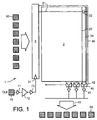
- a SRAM test chip 1 consists of a matrix memory array 2 which has an address register 3 connected to its plural wordlines 21, of which only one is shown.
- the wordlines 21 connect to a regular array of memory cells 22, of which again only one is shown.
- an exemplary memory cell 22 consists of two cross-coupled inverter circuits 26, 27; 28, 29.
- the left hand inverter as shown consists of a P channel FET 26 connected between a positive supply VDD and a first common node and an N channel FET 27 connected between the first common node and a negative supply VSS.
- the right hand inverter similarly consists of a second P conductivity FET 28 connected between the positive supply VDD and a second common node, and a second N channel FET 29 connected between the second common node and the negative supply VSS.
- the gates of the first P and first N transistors 26, 27 are connected together and to the second common node, and the gates of the second P transistor 28 and the second N transistor 29 are connected together and to the first common node.
- the first common node is connected via an N type pass transistor 24 to a first bitline 23 and the second common node is connected via a second N channel pass transistor 25 to a second bitline 24.
- the wordline 21 forms the gate connection to both the first and second pass transistors 24 and 25.
- the bitlines 23, 24 are complementary and form the column lines of the memory array whereas the wordlines form the row lines of the array.
- bitline 23 is connected to a logic 1 and bitline 24 to a logic 0
- the pass transistors 24, 25 will turn on and the cross-coupled inverters will latch into a corresponding state with the first common node at a high potential and the second common node at a low potential.
- the wordline is once again connected to a logic 1 and the pass transistors 24, 25 will then turn on causing the bitline potential to tend towards the respective potential of the common node to which it is connected.
- each pair of bitlines is connected to a respective sense amplifier 42.
- the output of the sense amplifier 40 feeds via a buffer 41 to a corresponding number of output pads 50.
- 32 pairs of bitlines are provided and thus there are 32 sense amplifiers 40, connected to 32 output terminals 50 via output circuitry 43.
- An input to the address register 3 is provided from a plurality of input pads 60 and the address register itself is clocked at an address register clock terminal 31.
- a clock input pad 70 is connected to the address register clock terminal 31 via a circuit path containing the three series elements 71, 72, 73 which figuratively illustrate the delay entailed.
- the sense amplifiers 40 are also clocked, each having a clock terminal 42.
- a clock pulse line 46 is connected between the address register 3 and the sense amplifier clock terminal 42, and has a delay sufficient to ensure that the sense amplifier 40 will operate correctly, as later described herein.
- a clock pulse 100 is provided at address register clock input pad 70. After passing through the series elements 71-73 the clock pulse becomes an internal clock pulse 101 at a time T1 after the instant of application of the clock pulse 100 at the pad 70.
- the time period T1 is the delay induced by the path comprising series elements 71-73.
- the action of the internal clock 101 on the address register 3 causes the register to apply a transition 102 to the wordlines 21 after a further time delay T2.
- This time delay T2 is predominantly due to the switching time of the address register 3.
- the transition 102 on the wordlines 21 causes the memory cells 22 to become connected to the complementary bitlines 23, 24.
- the bitlines 23, 24 have a relatively high capacitance and the memory cells 22 have a relatively low current driving capability which means that the change of potential of 104 is relatively slow.
- the sense amplifier 42 were activated before the differential Vdiff between the complementary bitlines had achieved a sufficiently high value, the sense amplifier might latch into an incorrect state. Accordingly, a clock pulse 105 is applied to the clock terminal 42 of the sense amplifiers 40 at a time T3 where it is expected that the bitlines will have a sufficiently high differential voltage to ensure correct sensing. In turn, the sense amplifiers require a further interval T4 before the outputs at the output nodes of the buffers 41 have achieved a reliable level. Finally, the data output circuitry 43 causes a yet further delay T5 before the response to the access caused by the clock pulse 100 applied to terminal 70 is accessible at the output pads 50.
- the clock pulse 105 is applied at a time sufficiently late to ensure that the sense amplifier will correctly sense the state of the bitlines. It is desirable to apply this clock pulse earlier whilst still retaining certainty that the correct sensing will occur.
- a first embodiment of the present invention has a multiplexer 90 providing an output to the clock terminal 42 of the sense amplifier 40, the two inputs to the multiplexer 90 being provided from the clock pulse line 46 and from an input pad 73.
- the multiplexer 90 is controlled by a multiplexer select pad 72.
- the output terminals of the sense amplifiers are connected to flip-flop circuitry 44 having a clock input 45 connected to a flip-flop circuitry clock pad 75.
- the circuitry stores at its outputs the states of its inputs immediately prior to the clock pulse.
- the flip-flop circuitry outputs connect via the data output circuitry 43 to the output pads 50.
- the multiplexer 90 is set by the multiplexer select node 72 to allow self clocking of the sense amplifiers from the clock line 46 of the memory.
- a timing signal 100 is applied to the address register clock input pad 70 at time T0 and this pulse will arrive at the address register clock node 31 as an internal clock pulse 101 at a time T1 determined by the delay caused by the path connecting the input pad 70 to the clock node 31.
- the sense amplifiers 42 are clocked at a still later time T3 with a sense amplifier clock 105.
- the inherent sense amplifier delay produces an output 106 at a yet later time T4 at the flip-flop inputs.
- the above described operation is performed successively while varying the instant of application of a second timing signal 107 to the flip-flop circuitry clock input pad 75.
- This pulse arrives at the flip-flop circuitry clock node 45 as an internal clock signal 108 after a delay Td.
- the timing is varied until Ta, the instant where the internal clock signal 108 is coincident with the sense amplifier output 106. This is sensed by varying the timing until the data output 109 at output pads 50 is just valid.
- just valid it is meant that any earlier application of the second timing signal 107 to input pad 75 would give rise to invalid data.
- the instant of application of the second timing signal 107 at pad 75 is then locked at Ta the just valid instant with respect to the time of application of the timing signal at address register clock pad 70 for the remainder of the test.
- a control signal is then applied to the multiplexer select pad 72 so as to switch multiplexer 90 over such that external clock signals supplied from the sense amplifier clock pad 73 are provided to the sense amplifiers 72.
- This valid output means that the external sense amplifier at the sense amplifier clock input 42 after the differential on the bitlines has built up enough to provide a valid output.
- the timing of the sense amplifier clock pulse is further delayed until it is determined that any further increase in delay would give rise to an invalid output at output pads 50 ie produces a latest just valid result. Since the flip-flop clock pulse has been maintained at its fixed timing Ta with respect to the input clock pulse applied to address register input pads 70, the "latest just valid" external sense amplifier clock occurs at the instant that the internally generated sense amplifier clock would have been applied over line 46.
- the delay of the externally applied sense amplifier clock is then successively reduced until again an invalid output occurs at the output pads 50 at an instant termed the earliest just valid instant.
- the invalidity is due to the sense amplifier 42 being clocked when an insufficient differential on the complementary bitlines 23, 24 exists.
- the time differential between the two "latest just valid” and “earliest just valid” extremes of the externally applied sense amplifier clock pulse represents the amount by which the internal sense amplifier clock over line 46 could be shortened in time whilst still achieving a valid output.
- the path length between the first clock input pad 70 and the address register clock input 31 and the path length between the sense amplifier clock pad 73 and the sense amplifier clock input 40 are set to be the same in which case it would be possible to determine absolutely the minimum possible time delay for clocking the sense amplifiers to ensure sufficient bitline differential had developed.
Landscapes
- For Increasing The Reliability Of Semiconductor Memories (AREA)
- Tests Of Electronic Circuits (AREA)
- Dram (AREA)
- Static Random-Access Memory (AREA)
Abstract
An apparatus and method for determining the minimum clock delay first of all determines the response time of the overall circuit by varying the application instant of an external clock until the circuit output is just valid. Then an external senseamp clock is substituted for the internal senseamp clock and the instant of application of the external clock is again varied until the circuit output is just valid. <IMAGE>
Description
The present invention relates to a method of operating a device
such as a memory, a testing device for a memory and to a method
of determining a minimum sense amplifier clock delay.
Semiconductor memories have a matrix of memory cells, the matrix
having rows formed by wordlines and columns formed by
complementary pairs of bitlines. The bitline pairs are connected
to clocked sense amplifiers which evaluate the contents of a cell
which is connected to the bitlines. The complementary bitlines
tend to have a high capacitance and the memory cells tend to have
a relatively low current driving capability which means that the
differential voltage across the complementary pair of bitlines
increases relatively slowly.
An ideal sense amplifier would be capable of connection to the
bitlines shortly after the memory cell was connected to them and
would then respond to the increasing differential voltage to
provide either a logic 1 or logic 0 output. However, sense
amplifiers normally have an input offset. This offset, which may
be positive or negative, must be overcome by the differential
voltage on the bitlines before the sense amplifier can latch into
the correct state.
For security it is therefore common practice to delay clocking
the sense amplifier until a large differential voltage has
developed across the complementary bitlines. This allows for
manufacturing tolerances. It also avoids the need for measuring
the minimum time needed for correct sensing to occur. Such a
measurement is difficult especially where the memory is embedded.
The present invention aims to provide a technique for determining
the minimum sense amplifier clock delay, which minimum delay
still gives rise to a correct output from the sense amplifier.
According to a first aspect of the present invention there is
provided a method of operating a device, the device comprising
circuitry having an input responsive to a first timing signal and
producing a valid output to clocked output circuitry after a
first delay, said clocked output circuitry having a clock node,
and a clock delay circuit responsive to said first timing signal
for providing at a second delay, a second timing signal to said
clock node of said clocked output circuitry, the method
comprising repeatedly applying said first timing signal followed
by an external timing signal, wherein said external timing signal
is applied via a delay-producing first path to said clock node;
monitoring an output of said clocked output circuitry; varying
the delay of application of said external timing signal with
respect to said first timing signal; and in response to a desired
output of said clocked output circuitry, modifying said second
delay.
Preferably said desired output is a just valid output such that
any reduced delay in said external timing signal gives rise to an
invalid output.
Advantageously before said repeatedly applying step said method
further comprises determining when said second timing signal
occurs and, during said repeatedly applying step, determining
when said desired output occurs.
Conveniently said step of determining when said second timing
signal occurs comprises providing latch circuitry responsive to
the output of said clocked output circuitry, said latch circuitry
having a latch clock node connected to a latch clock pad via a
delay producing second path; successively providing said second
timing signal to said clock node of said clocked output circuitry
and a latch timing signal to said latch clock pad; varying the
time of occurrence of said latch timing signal; and monitoring
the latch circuitry output.
Advantageously after said step of monitoring the latch circuitry
output, the method further comprises applying the externally
generated clock signal via the delay-producing first path to said
clock node and varying the time thereof; and monitoring the latch
circuitry output.
Conveniently said device is a memory comprising an address
register having a clock input, an array of memory cells having
wordlines connected to said address register, and plural bitlines
and clocked sense amplifiers for evaluating said bitlines.
According to a second aspect of the present invention there is
provided a method of determining a minimum sense amplifier clock
delay in a memory, the memory comprising address register
circuitry having a clock input, an array of memory cells having
wordlines coupled to said address register circuitry and bitlines
connected to sense amplifier circuitry, said sense amplifier
circuitry having a clock input, the memory further having output
circuitry having an input coupled to the output of said sense
amplifier circuitry and an output, the method comprising:-
Preferably said output circuitry has an output circuitry clock
input, said memory further comprises a sense amplifier clock
generator having an output, and said method comprises, before
said repeatedly applying step, the repeated steps of applying
first timing signals at said first path, and applying the output
of said sense amplifier clock pulse generator to said clock input
of said sense amplifier circuitry whilst varying the delay of
application of a timing signal with respect to said first timing
signal to said clock input of said output circuitry until a
desired output condition exists.
Advantageously said repeatedly applying step comprises applying
said timing signal to said output circuitry clock input at the
delay where said desired output condition exists.
Advantageously said desired condition is a condition where an
output is valid, but any reduction in said delay gives rise to an
invalid output.
According to a third aspect of the present invention there is
provided a testing device for a memory, said memory having
address register circuitry having an address register clock node,
a memory array and sense amplifier circuitry having a sense
amplifier clock node and a sense amplifier output, said testing
device comprising a first timing signal generator coupled to said
address register clock node via a first path for clocking said
address register circuitry, a sense amplifier clock generator
responsive to a signal at said address register clock node for
producing a first sense amplifier clock signal, a second timing
signal generator coupled to said sense amplifier clock node for
providing a second sense amplifier clock signal, clocking and
selector circuitry for selectably coupling said first or said
second sense amplifier clock signal, to said sense amplifier
clock node, said device further comprising means for varying the
relative timing of said first timing signal with respect to said
second timing signal.
Advantageously said testing device further comprises output
circuitry connected between said sense amplifier output and a
device output, and evaluating apparatus coupled to said device
output.
Conveniently said output circuitry comprises clocked latch
circuitry connected at said sense amplifier output, and having a
clock node coupled to receive a third timing signal.
An embodiment of the invention will now be described, by way of
example only, with reference to the accompanying drawings in
which:-
In the various figures, like reference numerals refer to like
parts.
Referring first to Figure 1 a SRAM test chip 1 consists of a
matrix memory array 2 which has an address register 3 connected
to its plural wordlines 21, of which only one is shown. The
wordlines 21 connect to a regular array of memory cells 22, of
which again only one is shown.
Referring now to Figure 2, an exemplary memory cell 22 consists
of two cross-coupled inverter circuits 26, 27; 28, 29. The left
hand inverter as shown consists of a P channel FET 26 connected
between a positive supply VDD and a first common node and an N
channel FET 27 connected between the first common node and a
negative supply VSS. The right hand inverter, as shown,
similarly consists of a second P conductivity FET 28 connected
between the positive supply VDD and a second common node, and a
second N channel FET 29 connected between the second common node
and the negative supply VSS. The gates of the first P and first
N transistors 26, 27 are connected together and to the second
common node, and the gates of the second P transistor 28 and the
second N transistor 29 are connected together and to the first
common node. The first common node is connected via an N type
pass transistor 24 to a first bitline 23 and the second common
node is connected via a second N channel pass transistor 25 to a
second bitline 24. The wordline 21 forms the gate connection to
both the first and second pass transistors 24 and 25. As is
known to those skilled in the art the bitlines 23, 24 are
complementary and form the column lines of the memory array
whereas the wordlines form the row lines of the array.
In operation, information is written into the memory cell 22 by
providing a differential potential on the bitlines 23, 24. If
for example bitline 23 is connected to a logic 1 and bitline 24
to a logic 0, then when the wordline 21 goes logic 1 the pass
transistors 24, 25 will turn on and the cross-coupled inverters
will latch into a corresponding state with the first common node
at a high potential and the second common node at a low
potential. To read from the memory the wordline is once again
connected to a logic 1 and the pass transistors 24, 25 will then
turn on causing the bitline potential to tend towards the
respective potential of the common node to which it is connected.
Returning again to Figure 1, each pair of bitlines is connected
to a respective sense amplifier 42. The output of the sense
amplifier 40 feeds via a buffer 41 to a corresponding number of
output pads 50.
In the illustrated embodiment, 32 pairs of bitlines are provided
and thus there are 32 sense amplifiers 40, connected to 32 output
terminals 50 via output circuitry 43.
An input to the address register 3 is provided from a plurality
of input pads 60 and the address register itself is clocked at an
address register clock terminal 31. A clock input pad 70 is
connected to the address register clock terminal 31 via a circuit
path containing the three series elements 71, 72, 73 which
figuratively illustrate the delay entailed.
The sense amplifiers 40 are also clocked, each having a clock
terminal 42. A clock pulse line 46 is connected between the
address register 3 and the sense amplifier clock terminal 42, and
has a delay sufficient to ensure that the sense amplifier 40 will
operate correctly, as later described herein.
Referring now to Figure 3, in operation, a clock pulse 100 is
provided at address register clock input pad 70. After passing
through the series elements 71-73 the clock pulse becomes an
internal clock pulse 101 at a time T1 after the instant of
application of the clock pulse 100 at the pad 70. The time
period T1 is the delay induced by the path comprising series
elements 71-73.
The action of the internal clock 101 on the address register 3
causes the register to apply a transition 102 to the wordlines 21
after a further time delay T2. This time delay T2 is
predominantly due to the switching time of the address register
3.
As previously discussed, the transition 102 on the wordlines 21
causes the memory cells 22 to become connected to the
complementary bitlines 23, 24. The bitlines 23, 24 have a
relatively high capacitance and the memory cells 22 have a
relatively low current driving capability which means that the
change of potential of 104 is relatively slow. If the sense
amplifier 42 were activated before the differential Vdiff between
the complementary bitlines had achieved a sufficiently high
value, the sense amplifier might latch into an incorrect state.
Accordingly, a clock pulse 105 is applied to the clock terminal
42 of the sense amplifiers 40 at a time T3 where it is expected
that the bitlines will have a sufficiently high differential
voltage to ensure correct sensing. In turn, the sense amplifiers
require a further interval T4 before the outputs at the output
nodes of the buffers 41 have achieved a reliable level. Finally,
the data output circuitry 43 causes a yet further delay T5 before
the response to the access caused by the clock pulse 100 applied
to terminal 70 is accessible at the output pads 50.
As noted above, the clock pulse 105 is applied at a time
sufficiently late to ensure that the sense amplifier will
correctly sense the state of the bitlines. It is desirable to
apply this clock pulse earlier whilst still retaining certainty
that the correct sensing will occur.
Referring now to Figure 4, a first embodiment of the present
invention has a multiplexer 90 providing an output to the clock
terminal 42 of the sense amplifier 40, the two inputs to the
multiplexer 90 being provided from the clock pulse line 46 and
from an input pad 73. The multiplexer 90 is controlled by a
multiplexer select pad 72.
The output terminals of the sense amplifiers are connected to
flip-flop circuitry 44 having a clock input 45 connected to a
flip-flop circuitry clock pad 75. When a clock pulse is applied
to the flip-flop circuitry 44, the circuitry stores at its
outputs the states of its inputs immediately prior to the clock
pulse. The flip-flop circuitry outputs connect via the data
output circuitry 43 to the output pads 50.
It will be understood by those skilled in the art that by varying
the time of application of the clock pulse at flip-flop circuitry
clock node 45, the timing of occurrence a successful memory
access can be determined. If the clock pulse is applied to flip-flop
circuitry clock node 45 before the sense amplifier outputs
are valid, then the flip-flop circuitry will store at its outputs
an invalid condition and this will be accessible at the output
pads 50. If the pulse is applied successively later, the
appearance of a valid output indicates the instant at which the
access has occurred.
Operation of the circuit of Figure 4 will now be described with
reference to Figure 5:-
In an initial test phase, the multiplexer 90 is set by the
multiplexer select node 72 to allow self clocking of the sense
amplifiers from the clock line 46 of the memory. A timing signal
100 is applied to the address register clock input pad 70 at time
T0 and this pulse will arrive at the address register clock node
31 as an internal clock pulse 101 at a time T1 determined by the
delay caused by the path connecting the input pad 70 to the clock
node 31.
As previously discussed, this will cause the wordline 21 to go to
logic high at a rising edge 102, at a somewhat later time T2 and,
allowing sufficient time for the bitlines 23, 24 to acquire a
sufficiently high differential, the sense amplifiers 42 are
clocked at a still later time T3 with a sense amplifier clock
105. The inherent sense amplifier delay produces an output 106
at a yet later time T4 at the flip-flop inputs.
The above described operation is performed successively while
varying the instant of application of a second timing signal 107
to the flip-flop circuitry clock input pad 75. This pulse
arrives at the flip-flop circuitry clock node 45 as an internal
clock signal 108 after a delay Td. The timing is varied until
Ta, the instant where the internal clock signal 108 is coincident
with the sense amplifier output 106. This is sensed by varying
the timing until the data output 109 at output pads 50 is just
valid. By "just valid" it is meant that any earlier application
of the second timing signal 107 to input pad 75 would give rise
to invalid data.
The instant of application of the second timing signal 107 at pad
75 is then locked at Ta the just valid instant with respect to
the time of application of the timing signal at address register
clock pad 70 for the remainder of the test.
A control signal is then applied to the multiplexer select pad 72
so as to switch multiplexer 90 over such that external clock
signals supplied from the sense amplifier clock pad 73 are
provided to the sense amplifiers 72.
Then operation of the circuit is resumed using the first timing
signal 100 applied to clock input pad 70 with the second timing
signal 107 provided to input pad 75 locked at the valid delay
after first timing signal 100, previously determined. Initially,
an external sense amplifier clock input is applied at sense
amplifier clock pad 73 and the time of application of this is
varied until a valid output is sensed at the output pads 50.
This valid output means that the external sense amplifier at the
sense amplifier clock input 42 after the differential on the
bitlines has built up enough to provide a valid output.
Once such a valid output is achieved, the timing of the sense
amplifier clock pulse is further delayed until it is determined
that any further increase in delay would give rise to an invalid
output at output pads 50 ie produces a latest just valid result.
Since the flip-flop clock pulse has been maintained at its fixed
timing Ta with respect to the input clock pulse applied to
address register input pads 70, the "latest just valid" external
sense amplifier clock occurs at the instant that the internally
generated sense amplifier clock would have been applied over line
46.
Having established this instant, the delay of the externally
applied sense amplifier clock is then successively reduced until
again an invalid output occurs at the output pads 50 at an
instant termed the earliest just valid instant. In this case,
the invalidity is due to the sense amplifier 42 being clocked
when an insufficient differential on the complementary bitlines
23, 24 exists.
The time differential between the two "latest just valid" and
"earliest just valid" extremes of the externally applied sense
amplifier clock pulse represents the amount by which the internal
sense amplifier clock over line 46 could be shortened in time
whilst still achieving a valid output.
Having determined this margin of timing, it may be possible to
reduce the delay induced by the clock pulse delay line 46. It
will be borne in mind of course that operating the sense
amplifier at exactly the "earliest just valid" minimum delay is
likely to be undesirable since some margin must be provided.
Those skilled in the art will appreciate that the circuit
described above, and the method of use is advantageous in that it
does not require absolute measurements to be made of any of the
delays in the circuit. Moreover, the path links for the various
externally applied clocks are not significant in the
measurements, which measurements allow the operating time margin
to be nonetheless accurately measured.
In a second embodiment, the path length between the first clock
input pad 70 and the address register clock input 31 and the path
length between the sense amplifier clock pad 73 and the sense
amplifier clock input 40 are set to be the same in which case it
would be possible to determine absolutely the minimum possible
time delay for clocking the sense amplifiers to ensure sufficient
bitline differential had developed.
Claims (12)
- A method of operating a device, the device comprising circuitry having an input responsive to a first timing signal and producing a valid output to clocked output circuitry after a first delay, said clocked output circuitry having a clock node, and a clock delay circuit responsive to said first timing signal for providing at a second delay, a second timing signal to said clock node of said clocked output circuitry, the method comprising:-repeatedly applying said first timing signal followed by an external timing signal, wherein said external timing signal is applied via a delay-producing first path to said clock node;monitoring an output of said clocked output circuitry;varying the delay of application of said external timing signal with respect to said first timing signal; andin response to a desired output of said clocked output circuitry, modifying said second delay.
- The method of claim 1, wherein said desired output is a just valid output such that any reduced delay in said external timing signal gives rise to an invalid output.
- The method of claim 2 comprising, before said repeatedly applying step, determining when said second timing signal occurs and, during said repeatedly applying step, determining when said desired output occurs.
- The method of claim 3, wherein said step of determining when said second timing signal occurs comprises:-providing latch circuitry responsive to the output of said clocked output circuitry, said latch circuitry having a latch clock node connected to a latch clock pad via a delay producing second path;repeatedly providing said second timing signal to said clock node of said clocked output circuitry and a latch timing signal to said latch clock pad;varying the time of occurrence of said latch timing signal; andmonitoring the latch circuitry output.
- The method of claim 4, further comprising after said step of monitoring the latch circuitry output, applying the externally generated clock signal via the delay-producing first path to said clock node and varying the time thereof;monitoring said latch circuitry output.
- The method of any preceding claim, wherein said device is a memory comprising an address register having a clock input, an array of memory cells having wordlines connected to said address register, and plural bitlines and clocked sense amplifiers for evaluating said bitlines.
- A method of determining a minimum sense amplifier clock delay in a memory, the memory comprising address register circuitry having a clock input, an array of memory cells having wordlines coupled to said address register circuitry and bitlines connected to sense amplifier circuitry, said sense amplifier circuitry having a clock input, the memory further having output circuitry having an input coupled to the output of said sense amplifier circuitry and an output, the method comprising:-providing a first path having an input, said first path having an output coupled to said clock input of said address register circuitry;providing a second path having an input, said second path having an output coupled to said clock input of said sense amplifier circuitry;repeatedly applying first timing signals at said input of said first path and at a variable delay after each said application, applying a second timing signal at said input of said second path; andevaluating conditions at said output of said output circuitry.
- The method of claim 7, wherein said output circuitry has an output circuitry clock input, said memory further comprises a sense amplifier clock generator having an output, and said method comprises, before said repeatedly applying step, the repeated steps of applying first timing signals at said first path, and applying the output of said sense amplifier clock pulse generator to said clock input of said sense amplifier circuitry whilst varying the delay of application of a timing signal with respect to said first timing signal to said clock input of said output circuitry until a desired output condition exists.
- The method of claim 8, wherein said repeatedly applying step comprises applying said timing signal to said output circuitry clock input at the delay where said desired output condition exists.
- A testing device for a memory said memory having address register circuitry having an address register clock node, a memory array and sense amplifier circuitry having a sense amplifier clock node and a sense amplifier output, said testing device comprising a first timing signal generator coupled to said address register clock node via a first path for clocking said address register circuitry, a sense amplifier clock generator responsive to a signal at said address register clock node for producing a first sense amplifier clock signal, a second timing signal generator coupled to said sense amplifier clock node for providing a second sense amplifier clock signal, clocking and selector circuitry for selectably coupling said first or said second sense amplifier clock signal, to said sense amplifier clock node, said device further comprising means for varying the relative timing of said first timing signal with respect to said second timing signal.
- The testing device of claim 10, further comprising output circuitry connected between said sense amplifier output and a device output, and evaluating apparatus coupled to said device output.
- The device of claim 10 or 11, wherein said output circuitry comprises clocked latch circuitry connected at said sense amplifier output, and having a clock node coupled to receive a third timing signal.
Applications Claiming Priority (2)
| Application Number | Priority Date | Filing Date | Title |
|---|---|---|---|
| GB9914069 | 1999-06-16 | ||
| GBGB9914069.1A GB9914069D0 (en) | 1999-06-16 | 1999-06-16 | Memory testing |
Publications (1)
| Publication Number | Publication Date |
|---|---|
| EP1061528A1 true EP1061528A1 (en) | 2000-12-20 |
Family
ID=10855495
Family Applications (1)
| Application Number | Title | Priority Date | Filing Date |
|---|---|---|---|
| EP00302825A Withdrawn EP1061528A1 (en) | 1999-06-16 | 2000-04-04 | Memory testing |
Country Status (3)
| Country | Link |
|---|---|
| US (1) | US6604213B1 (en) |
| EP (1) | EP1061528A1 (en) |
| GB (1) | GB9914069D0 (en) |
Families Citing this family (3)
| Publication number | Priority date | Publication date | Assignee | Title |
|---|---|---|---|---|
| JP4480238B2 (en) * | 2000-07-18 | 2010-06-16 | Okiセミコンダクタ株式会社 | Semiconductor device |
| US7269524B1 (en) * | 2006-06-30 | 2007-09-11 | Inapac Technology, Inc. | Delay lock loop delay adjusting method and apparatus |
| US20080211569A1 (en) * | 2007-03-01 | 2008-09-04 | Hui Kelvin Yupak | Higher voltage switch based on a standard process |
Citations (6)
| Publication number | Priority date | Publication date | Assignee | Title |
|---|---|---|---|---|
| US5576996A (en) * | 1994-09-12 | 1996-11-19 | Fujitsu Limited | Semiconductor memory device having a variably write pulse width capability |
| EP0867887A2 (en) * | 1997-03-14 | 1998-09-30 | Texas Instruments Incorporated | Memory access time measurement circuit and method |
| EP0874370A1 (en) * | 1997-04-25 | 1998-10-28 | STMicroelectronics, Inc. | Sense amplifier control of a memory device |
| WO1999004400A2 (en) * | 1997-07-16 | 1999-01-28 | Tanisys Technology, Inc. | Synchronous memory identification system |
| US5875135A (en) * | 1995-12-28 | 1999-02-23 | Intel Corporation | Characterization of self time circuit |
| EP0898284A2 (en) * | 1997-07-31 | 1999-02-24 | Nec Corporation | Semiconductor memory having a test circuit |
Family Cites Families (1)
| Publication number | Priority date | Publication date | Assignee | Title |
|---|---|---|---|---|
| US6421801B1 (en) * | 1999-06-08 | 2002-07-16 | Intel Corporation | Testing IO timing in a delay locked system using separate transmit and receive loops |
-
1999
- 1999-06-16 GB GBGB9914069.1A patent/GB9914069D0/en not_active Ceased
-
2000
- 2000-04-04 EP EP00302825A patent/EP1061528A1/en not_active Withdrawn
- 2000-04-11 US US09/546,810 patent/US6604213B1/en not_active Expired - Fee Related
Patent Citations (6)
| Publication number | Priority date | Publication date | Assignee | Title |
|---|---|---|---|---|
| US5576996A (en) * | 1994-09-12 | 1996-11-19 | Fujitsu Limited | Semiconductor memory device having a variably write pulse width capability |
| US5875135A (en) * | 1995-12-28 | 1999-02-23 | Intel Corporation | Characterization of self time circuit |
| EP0867887A2 (en) * | 1997-03-14 | 1998-09-30 | Texas Instruments Incorporated | Memory access time measurement circuit and method |
| EP0874370A1 (en) * | 1997-04-25 | 1998-10-28 | STMicroelectronics, Inc. | Sense amplifier control of a memory device |
| WO1999004400A2 (en) * | 1997-07-16 | 1999-01-28 | Tanisys Technology, Inc. | Synchronous memory identification system |
| EP0898284A2 (en) * | 1997-07-31 | 1999-02-24 | Nec Corporation | Semiconductor memory having a test circuit |
Also Published As
| Publication number | Publication date |
|---|---|
| US6604213B1 (en) | 2003-08-05 |
| GB9914069D0 (en) | 1999-08-18 |
Similar Documents
| Publication | Publication Date | Title |
|---|---|---|
| US5424985A (en) | Compensating delay element for clock generation in a memory device | |
| US6385101B1 (en) | Programmable delay control for sense amplifiers in a memory | |
| US5325337A (en) | Random access memories (RAM) and more particularly to self-timed RAMS | |
| JP2724893B2 (en) | Semiconductor integrated circuit device | |
| US20020144170A1 (en) | Computer system having memory device with adjustable data clocking using pass gates | |
| KR100328161B1 (en) | Integrated circuit memory | |
| HK1008758B (en) | Self-timed random access memories | |
| KR100331522B1 (en) | Write driver and bit line precharge apparatus and method | |
| KR960003533B1 (en) | Semiconductor memory device including address transition detector | |
| US20020080668A1 (en) | Current controlled multi-state parallel test for semiconductor device | |
| KR100197770B1 (en) | Semiconductor memory | |
| US6255862B1 (en) | Latch type sense amplifier circuit | |
| KR20040010724A (en) | Duty-cycle-efficient sram cell test | |
| KR19990040299A (en) | A semiconductor memory device having a clock synchronous precharge data input / output line and a data input / output line precharge method using the same | |
| KR100383007B1 (en) | Semiconductor storage device | |
| US5007028A (en) | Multiport memory with improved timing of word line selection | |
| US6604213B1 (en) | Method and apparatus for determining a minimum clock delay in a memory | |
| US5978286A (en) | Timing control of amplifiers in a memory | |
| US5365482A (en) | Semiconductor memory device with provision of pseudo-acceleration test | |
| KR100328160B1 (en) | Memory with bit line load with automatic bit line precharge and equalization | |
| US7075854B2 (en) | Semiconductor memory device, write control circuit and write control method for the same | |
| US6359816B1 (en) | Response time measurement | |
| US6584577B1 (en) | System for measuring response time of a circuit by determining the time difference between the earlier and the later clock pulses applied to the circuit | |
| US5629896A (en) | Write controlled address buffer | |
| US5422851A (en) | Semiconductor memory device capable of verifying use of redundant circuit |
Legal Events
| Date | Code | Title | Description |
|---|---|---|---|
| PUAI | Public reference made under article 153(3) epc to a published international application that has entered the european phase |
Free format text: ORIGINAL CODE: 0009012 |
|
| AK | Designated contracting states |
Kind code of ref document: A1 Designated state(s): DE FR GB IT |
|
| AX | Request for extension of the european patent |
Free format text: AL;LT;LV;MK;RO;SI |
|
| 17P | Request for examination filed |
Effective date: 20010525 |
|
| AKX | Designation fees paid |
Free format text: DE FR GB IT |
|
| 17Q | First examination report despatched |
Effective date: 20070212 |
|
| STAA | Information on the status of an ep patent application or granted ep patent |
Free format text: STATUS: THE APPLICATION IS DEEMED TO BE WITHDRAWN |
|
| 18D | Application deemed to be withdrawn |
Effective date: 20071101 |