EP1061526A1 - On chip data comparator with variable data and compare result compression - Google Patents
On chip data comparator with variable data and compare result compression Download PDFInfo
- Publication number
- EP1061526A1 EP1061526A1 EP00106931A EP00106931A EP1061526A1 EP 1061526 A1 EP1061526 A1 EP 1061526A1 EP 00106931 A EP00106931 A EP 00106931A EP 00106931 A EP00106931 A EP 00106931A EP 1061526 A1 EP1061526 A1 EP 1061526A1
- Authority
- EP
- European Patent Office
- Prior art keywords
- state
- data
- recited
- chip
- memory chip
- Prior art date
- Legal status (The legal status is an assumption and is not a legal conclusion. Google has not performed a legal analysis and makes no representation as to the accuracy of the status listed.)
- Granted
Links
- 238000007906 compression Methods 0.000 title description 10
- 230000006835 compression Effects 0.000 title description 10
- 230000015654 memory Effects 0.000 claims abstract description 100
- 238000012360 testing method Methods 0.000 claims abstract description 63
- 239000004065 semiconductor Substances 0.000 claims abstract description 32
- 238000013144 data compression Methods 0.000 claims description 21
- 230000002950 deficient Effects 0.000 claims description 4
- 238000010586 diagram Methods 0.000 description 4
- 238000004891 communication Methods 0.000 description 3
- 230000007547 defect Effects 0.000 description 3
- 230000001360 synchronised effect Effects 0.000 description 3
- 238000004519 manufacturing process Methods 0.000 description 2
- 230000004913 activation Effects 0.000 description 1
- 238000003491 array Methods 0.000 description 1
- 230000008859 change Effects 0.000 description 1
- 238000006243 chemical reaction Methods 0.000 description 1
- 238000011161 development Methods 0.000 description 1
- 230000006870 function Effects 0.000 description 1
- 238000000034 method Methods 0.000 description 1
- 238000012986 modification Methods 0.000 description 1
- 230000004048 modification Effects 0.000 description 1
Images

Classifications
-
- G—PHYSICS
- G11—INFORMATION STORAGE
- G11C—STATIC STORES
- G11C29/00—Checking stores for correct operation ; Subsequent repair; Testing stores during standby or offline operation
- G11C29/04—Detection or location of defective memory elements, e.g. cell constructio details, timing of test signals
- G11C29/08—Functional testing, e.g. testing during refresh, power-on self testing [POST] or distributed testing
- G11C29/12—Built-in arrangements for testing, e.g. built-in self testing [BIST] or interconnection details
- G11C29/36—Data generation devices, e.g. data inverters
-
- G—PHYSICS
- G11—INFORMATION STORAGE
- G11C—STATIC STORES
- G11C29/00—Checking stores for correct operation ; Subsequent repair; Testing stores during standby or offline operation
- G11C29/04—Detection or location of defective memory elements, e.g. cell constructio details, timing of test signals
- G11C29/08—Functional testing, e.g. testing during refresh, power-on self testing [POST] or distributed testing
- G11C29/12—Built-in arrangements for testing, e.g. built-in self testing [BIST] or interconnection details
- G11C29/38—Response verification devices
- G11C29/40—Response verification devices using compression techniques
Definitions
- This disclosure relates to semiconductor memory testing and more particularly, to an apparatus for testing memory devices using an on chip data comparison between input and output data patterns.
- a chip In semiconductor memory testing, a chip is tested by writing a known data pattern to memory cells in the array by an external testing device. The data pattern is then read back to the device and compared to the known data pattern.
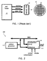
- a chip package 10 including a memory chip(s) 14 or a wafer 12 including a plurality of chips 14 may be tested using an external memory tester 16.
- tester 16 writes a specific pattern to the memory, reads the data back from the array and compares the original data pattern with the data read from the memory chip.
- any discrepancies are reported and used to determine pass/fail criteria for the memory chips (if no module level redundancy is available), and in the case of wafer testing, a bit fail map is generated.
- a x32 memory chip 32 I/O channels are needed for communication between each memory chip 14 and tester 16.
- a semiconductor memory chip in accordance with the present invention, includes a memory array including memory components to be tested.
- a pattern generator provides reference data to be input to and stored in the memory array.
- a comparator is formed on the memory chip for comparing the reference data from the pattern generator and the stored data from the memory array.
- the comparator further includes logic circuitry for comparing the reference data to the stored data from the memory array to provide a compare result having a matched state if the stored data matches the reference data and otherwise an unmatched state.
- a plurality of latches are included for receiving the compare result from the logic circuitry, the latches having a first state associated with the matched state wherein the first state is altered to a second state if the unmatched state is received from the logic circuitry.
- a register for storing and outputting the first and second states of the latches to provide a test result is also included.
- Another semiconductor memory chip includes a memory array including memory components to be tested and redundancies for replacement of defective memory components, the redundancies each including a set of components.
- a pattern generator is included for providing reference data to be input to and stored in the memory array, and a comparator is formed on the memory chip for comparing the reference data from the pattern generator and the stored data from the memory array.
- the comparator further includes logic circuitry for comparing the reference data set to the stored data from the memory array to provide compare results having a matched state if the stored data matches the reference data and otherwise an unmatched state.
- a multiplexer stage is included for receiving the compare results and compressing the compare results to provide redundancy compatible data compression such that any unmatched state associated with any components of a set of components permits replacement with a redundancy of the same size as the set of components.
- a plurality of latches receives the compare results from the multiplexer stage, the latches having a first state associated with the matched state wherein the first state is altered to a second state if the unmatched state is received from the logic circuitry.
- a register is also include for storing and outputting the first and second states of the latches to provide a test result.
- a synchronization stage is included for synchronizing compare results output from the logic circuitry.
- a multiplexer stage receives the compare results associated with each memory component and compresses the compare results for each memory component to provide redundancy compatible data compression such that any unmatched state associated with any components of a set of components permits replacement with a redundancy of the same size as the set of components.
- a plurality of latches is included for receiving the compare results from the multiplexer stage. The latches have a first state associated with the matched state wherein the first state is altered to a second state if the unmatched state is received from the logic circuitry.
- a shift register is included for storing and outputting the first and second states of the latches to provide a test result.
- the logic circuitry preferably includes one of an exclusive or gate and an exclusive nor gate, the gates including inputs for reference data and store data from the memory array.
- the semiconductor memory chip may further include a synchronization stage for synchronizing compare results output from the logic circuitry.
- the semiconductor memory chip may further included a multiplexer for receiving compare results from the logic circuitry and compressing the compare results to provide redundancy compatible data compression.
- the redundancy compatible data compression may be employed for testing one of wordlines, column select lines and memory banks.
- the semiconductor memory chip may include an on chip logic circuit for resetting the latches to the first state before compare cycles or an off chip external control device for resetting the latches to the first state before compare cycles.
- the register preferably includes a shift register and the test result may be compressed to a single bit, or the test result may be serially transmitted.
- the comparator is preferably coupled to read/write data lines to obtain the stored data from the memory array.
- the logic circuitry preferably includes one of an exclusive or gate and an exclusive nor gate, the gates including inputs for reference data and store data from the memory array.
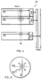
- Semiconductor memory device 100 includes a memory array including memory cells (not shown). Data is sent to and from memory cells on Read/Write Datalines (RWDs). Semiconductor memory device 100 includes an on chip data comparator 110 thereon in accordance with the present invention.
- Comparator 110 is coupled directly to a data path of memory chip 100 by, for example, connecting comparator 110 to Read/Write Datalines (RWDs) of memory chip 100.
- a pattern generator 112 provides pattern data bits (reference pattern) to both the memory array via RWD and to comparator 110.
- the reference pattern may be stored inside a memory 111 of comparator 110 from a previous write operation or generated by an on-chip pattern generator.
- Reference pattern data as well as array data are input to comparator 110 for comparison.
- An output compression input sets a compression mode for data results to be transmitted from comparator 110.
- the output compression input may be set by selecting a test mode for the operation of the test of memory chip 100. In this way no I/O pin is needed to set the compression mode.
- a strobe input is also provided for comparator 110.
- Strobe provided synchronization between array and reference data for the comparison performed by comparator 110.
- An interface such as a serial interface, between an external tester and the chip(s) to be tested, reduces the number of communication channels needed to test each memory chip 100 to 2, i.e., strobe and result.
- the result output may include a single bit representing a pass/fail criteria or additional information depending on the mode selected.
- comparator 110 is shown in greater detail in accordance with the present invention.
- a comparator stage 120 includes a plurality of logic comparators 122.
- Each comparator 122 may include a exclusive or (XOR) or an exclusive nor (XNOR) gates.
- Each comparator 122 receives input from the reference data path (pattern generator, preferably an on chip pattern generator) and from the array data path (from RWDs for example). The inputs are compared in comparator stage 120.
- a synchronization stage 130 synchronizes data from the array with the reference data (from pattern generator). Synchronization stage 130 is optional since array data and reference data may already be synchronized. Synchronization stage may include a plurality of switches 132 which preferably include transistor enabled by a gate signal. Gate signal is provided by an on chip control logic circuit 134 or by an external tester via an I/O pin.
- Multiplexer stage 140 may also be included. Multiplexer stage 140 is preferably employed to permit a redundancy compatible data compression scheme. This will be explained in greater detail below.
- Output of comparators 122 includes a compare result.
- the compare result defines a state for latches 152 included in latch stage 150.
- Latches 152 are reset or initialized before each compare cycle starts.
- a compare cycle may include a single test or a set of tests for testing (comparing) one or more memory cells on each chip or all the cells on each chip to the data pattern.
- Single memory cells or groups of memory cells can be tested, and the results of the test are compressed according to a selected compression ratio such that bits are output to latches 152 representing a single memory cell, a group of memory cells or all memory cells on a chip, as determined based on the compression ratio. This provides the compare result.
- Latches are preferably reset using a reset signal which is provided by on chip control logic circuit 134 or by the external tester via an I/O pin prior to the compare cycle.
- a reset signal which is provided by on chip control logic circuit 134 or by the external tester via an I/O pin prior to the compare cycle.
- latches 152 remain in the same initialized state. If the comparison between reference data and the array data is "bad", i.e., the data does not match, latches 152 change states to a non-initialize state.
- Each latch 152 functions individually and changes state independently based on comparison results from comparators 122. Only a "bad result changes the state of each latch 152. This feature of the present invention permits flexibility for data compression as will be described below in greater detail.
- a register stage 160 preferably includes a shift register 162. All latches 152 are connected to shift register 162. Shift register 162 performs parallel to serial conversions of the compare result provided by comparators 122. In one embodiment, the compare result is compressed to a single bit when only a pass/fail result is needed for the memory array being tested.
- a switch 164 is included to provide a way of selecting the output or data compression type used as the test result. In a first type of data compression, the data in shift register 162 is summed by a summer 166 and output as a single bit, for example a 0 or a 1. Shift register 162 is synchronized by an SR-clock signal input thereto.
- a zero sum is a pass test result while a non-zero sum is a fail test result.
- the values in shift register 162 are output directly providing more detailed test information.
- Switch 164 is activated by a user selected mode which provides an output compression signal in accordance therewith.
- Memory array 170 includes secondary sense amplifiers SSA which drive the RWDs.
- On chip data comparator 110 FIG. 3 advantageously permits extremely flexible data compression based on addressing schemes.
- a wordline WL and a column select line CSL are activated.
- the activation of a CSL and a WL results in accessing 4 memory cells a1-a4, i.e., a set.
- There memory cells are therefore not independent of each other. Whenever one of cells a1-a4 is addresses, all four cells are accessed. This is also true for redundant memory array elements.
- the data compression is controlled by latches 152. All compare results are accumulated in latches 152, until a reset signal from an external memory tester or from an on chip logic circuit reinitializes the latches as described above.
- the present invention advantageously utilizes the latch states to identify defects in any elements of the memory array. For example, addressing methods and data patterns may be implemented to provide defect checks on complete wordlines, of column select lines, of memory banks or other arbitrary portions of the array.
- a set of memory components are tested using comparators 122.
- the set of memory components which are compatible to the replacement size of redundancies which would be used to replace the set of components, have their compare results multiplexed by multiplexer 140 to compress the bits to a single compare result. In other words, if one of the set fails the entire set is considered to fail thereby significantly compressing the data output for test results.
- channels normally used for comparing array data to reference data become available. For example, about 31 channels are available per chip in a typically setup (See FIG. 1). This means the tester may now test significantly more than 7 chips in parallel thereby increasing throughput for acceptance testing of memory chips. Even further improvements may be realized if aan on chip pattern generator is employed.
Landscapes
- Tests Of Electronic Circuits (AREA)
- For Increasing The Reliability Of Semiconductor Memories (AREA)
- Dram (AREA)
- Techniques For Improving Reliability Of Storages (AREA)
Abstract
Description
Claims (26)
- A semiconductor memory chip comprising:a memory array including memory components to be tested;a pattern generator for providing reference data to be input to and stored in the memory array; anda comparator formed on the memory chip for comparing the reference data from the pattern generator and the stored data from the memory array, the comparator further comprising:logic circuitry for comparing the reference data to the stored data from the memory array to provide compare results having a matched state if the stored data matches the reference data and otherwise an unmatched state;a plurality of latches for receiving the compare results from the logic circuitry, the latches having a first state associated with the matched state wherein the first state is altered to a second state if the unmatched state is received from the logic circuitry; anda register for storing and outputting the first and second states of the latches to provide a test result.
- The semiconductor memory chip as recited in claim 1, wherein the logic circuitry includes one of an exclusive or gate and an exclusive nor gate, the gates including inputs for reference data and store data from the memory array.
- The semiconductor memory chip as recited in claim 1, further comprises a synchronization stage for synchronizing the compare results output from the logic circuitry.
- The semiconductor memory chip as recited in claim 1, further comprises a multiplexer for receiving the compare results from the logic circuitry and compressing the compare results to provide redundancy compatible data compression.
- The semiconductor memory chip as recited in claim 4, wherein the redundancy compatible data compression is employed for testing one of wordlines, column select lines and memory banks.
- The semiconductor memory chip as recited in claim 1, further comprises an on chip logic circuit for resetting the latches to the first state before compare cycles.
- The semiconductor memory chip as recited in claim 1, further comprises an off chip external control device for resetting the latches to the first state before compare cycles.
- The semiconductor memory chip as recited in claim 1, wherein the register includes a shift register and the test result is compressed to a single bit.
- The semiconductor memory chip as recited in claim 1, wherein the register includes a shift register and the test result is serially transmitted.
- The semiconductor memory chip as recited in claim 1, wherein the comparator is coupled to read/write data lines to obtain the stored data from the memory array.
- A semiconductor memory chip comprising:a memory array including memory components to be tested and redundancies for replacement of defective memory components, the redundancies each including a set of components;a pattern generator for providing reference data to be input to and stored in the memory array; anda comparator formed on the memory chip for comparing the reference data from the pattern generator and the stored data from the memory array, the comparator further comprising:logic circuitry for comparing the reference data to the stored data from the memory array to provide compare results having a matched state if the stored data matches the reference data and otherwise an unmatched state;a multiplexer stage for receiving the compare results and compressing the compare results to provide redundancy compatible data compression such that any unmatched state associated with any components of a set of components permits replacement with a redundancy of the same size as the set of components;a plurality of latches for receiving the compare results from the multiplexer stage, the latches having a first state associated with the matched state wherein the first state is altered to a second state if the unmatched state is received from the logic circuitry; anda register for storing and outputting the first and second states of the latches to provide a test result.
- The semiconductor memory chip as recited in claim 11, wherein the logic circuitry includes one of an exclusive or gate and an exclusive nor gate, the gates including inputs for reference data and store data from the memory array.
- The semiconductor memory chip as recited in claim 11, further comprises a synchronization stage for synchronizing compare results output from the logic circuitry.
- The semiconductor memory chip as recited in claim 11, wherein the redundancy compatible data compression is employed for testing one of wordlines, column select lines and memory banks.
- The semiconductor memory chip as recited in claim 11, further comprises an on chip logic circuit for resetting the latches to the first state before compare cycles.
- The semiconductor memory chip as recited in claim 11, further comprises an off chip external control device for resetting the latches to the first state before compare cycles.
- The semiconductor memory chip as recited in claim 11, wherein the register includes a shift register and the test result is compressed to a single bit.
- The semiconductor memory chip as recited in claim 11, wherein the register includes a shift register and the test result is serially transmitted.
- The semiconductor memory chip as recited in claim 11, wherein the comparator is coupled to read/write data lines to obtain the stored data from the memory array.
- A DRAM memory chip comprising:a memory array including memory components to be tested and redundancies for replacement of defective memory components, the redundancies each including a set of components;a pattern generator included on the memory chip for providing a reference data to be input to and stored in the memory array; anda comparator formed on the memory chip for comparing the reference data set from the pattern generator and the stored data from the memory array, the comparator being coupled to read/write data lines of the memory array for retrieving the stored data from the memory array, the comparator further comprising:logic circuitry for comparing the reference data to the stored data from the memory array to provide compare results having a matched state if the stored data matches the reference data and otherwise an unmatched state;a synchronization stage for synchronizing the compare results output from the logic circuitry,a multiplexer stage for receiving the compare results associated with each memory component and compressing the compare results for each memory component to provide redundancy compatible data compression such that any unmatched state associated with any components of a set of components permits replacement with a redundancy of the same size as the set of components;a plurality of latches for receiving the compare result from the multiplexer stage, the latches having a first state associated with the matched state wherein the first state is altered to a second state if the unmatched state is received from the logic circuitry; anda shift register for storing and outputting the first and second states of the latches to provide a test result.
- The DRAM memory chip as recited in claim 20, wherein the logic circuitry includes one of an exclusive or gate and an exclusive nor gate, the gates including inputs for reference data and store data from the memory array.
- The DRAM memory chip as recited in claim 20, wherein the redundancy compatible data compression is employed for testing one of wordlines, column select lines and memory banks.
- The DRAM memory chip as recited in claim 20, further comprises an on chip logic circuit for resetting the latches to the first state before compare cycles.
- The DRAM memory chip as recited in claim 20, further comprises an off chip external control device for resetting the latches to the first state before compare cycles.
- The DRAM memory chip as recited in claim 20, wherein the test result is compressed to a single bit.
- The DRAM memory chip as recited in claim 20, wherein the test result is serially transmitted.
Applications Claiming Priority (2)
| Application Number | Priority Date | Filing Date | Title |
|---|---|---|---|
| US313016 | 1999-05-17 | ||
| US09/313,016 US6357027B1 (en) | 1999-05-17 | 1999-05-17 | On chip data comparator with variable data and compare result compression |
Publications (2)
| Publication Number | Publication Date |
|---|---|
| EP1061526A1 true EP1061526A1 (en) | 2000-12-20 |
| EP1061526B1 EP1061526B1 (en) | 2008-08-27 |
Family
ID=23214023
Family Applications (1)
| Application Number | Title | Priority Date | Filing Date |
|---|---|---|---|
| EP00106931A Expired - Lifetime EP1061526B1 (en) | 1999-05-17 | 2000-03-31 | On chip data comparator with variable data and compare result compression |
Country Status (7)
| Country | Link |
|---|---|
| US (1) | US6357027B1 (en) |
| EP (1) | EP1061526B1 (en) |
| JP (1) | JP2001006394A (en) |
| KR (1) | KR20010014921A (en) |
| CN (1) | CN1174426C (en) |
| DE (1) | DE60040035D1 (en) |
| TW (1) | TW466499B (en) |
Cited By (2)
| Publication number | Priority date | Publication date | Assignee | Title |
|---|---|---|---|---|
| DE10338678A1 (en) * | 2003-08-22 | 2005-03-31 | Infineon Technologies Ag | Apparatus and method for testing circuit units to be tested |
| CN108351818A (en) * | 2015-11-02 | 2018-07-31 | 高通股份有限公司 | System and method for realizing error correcting code in memory |
Families Citing this family (31)
| Publication number | Priority date | Publication date | Assignee | Title |
|---|---|---|---|---|
| US6651203B1 (en) * | 1999-05-17 | 2003-11-18 | Infineon Technologies Ag | On chip programmable data pattern generator for semiconductor memories |
| US6578169B1 (en) * | 2000-04-08 | 2003-06-10 | Advantest Corp. | Data failure memory compaction for semiconductor test system |
| JP2002123562A (en) * | 2000-07-31 | 2002-04-26 | Hitachi Ltd | Method of generating tester construction data, method of constructing tester, and test circuit |
| US6754867B2 (en) * | 2000-12-28 | 2004-06-22 | Intel Corporation | Method of determining non-accessible device I/O pin speed using on chip LFSR and MISR as data source and results analyzer respectively |
| KR100410554B1 (en) * | 2001-07-13 | 2003-12-18 | 삼성전자주식회사 | method for outputting package map information in semiconductor memory device and circuit therefor |
| KR100442958B1 (en) * | 2001-12-10 | 2004-08-04 | 주식회사 하이닉스반도체 | Compress I/O circuit of Semiconductor memory device |
| US6714469B2 (en) * | 2002-07-02 | 2004-03-30 | Agilent Technologies, Inc. | On-chip compression of charge distribution data |
| US7047458B2 (en) * | 2002-12-16 | 2006-05-16 | Intel Corporation | Testing methodology and apparatus for interconnects |
| US7155370B2 (en) * | 2003-03-20 | 2006-12-26 | Intel Corporation | Reusable, built-in self-test methodology for computer systems |
| US7464307B2 (en) * | 2003-03-25 | 2008-12-09 | Intel Corporation | High performance serial bus testing methodology |
| US7137049B2 (en) | 2003-04-29 | 2006-11-14 | Infineon Technologies Ag | Method and apparatus for masking known fails during memory tests readouts |
| US6999887B2 (en) * | 2003-08-06 | 2006-02-14 | Infineon Technologies Ag | Memory cell signal window testing apparatus |
| DE10337854A1 (en) * | 2003-08-18 | 2005-03-31 | Infineon Technologies Ag | Integrated memory with a test circuit for the function test of the memory |
| US20050080581A1 (en) * | 2003-09-22 | 2005-04-14 | David Zimmerman | Built-in self test for memory interconnect testing |
| DE10356359A1 (en) * | 2003-11-28 | 2005-06-30 | Infineon Technologies Ag | Semiconductor memory analyzing method, involves compressing comparison bit sequence, such that sequence bits are linked with logic operation, and stopping production and display of parity bit for relative cell in one operation mode |
| US7251757B2 (en) * | 2003-12-02 | 2007-07-31 | International Business Machines Corporation | Memory testing |
| DE102004042252A1 (en) * | 2004-09-01 | 2005-11-10 | Infineon Technologies Ag | Integrated memory circuit has error recognition unit with compression memory unit for bitline values and error data comparison unit |
| US7263638B2 (en) * | 2004-12-16 | 2007-08-28 | Infineon Technologies Ag | Memory having test circuit |
| JP2007058450A (en) * | 2005-08-23 | 2007-03-08 | Freescale Semiconductor Inc | Semiconductor integrated circuit |
| KR100830958B1 (en) * | 2006-10-09 | 2008-05-20 | 주식회사디아이 | Apparatus and method for determining test results of semiconductor memory devices |
| US20080133175A1 (en) * | 2006-12-03 | 2008-06-05 | Lobuono Mark Anthony | Test interface for software-based sequence of event recording systems |
| US7665003B2 (en) * | 2006-12-15 | 2010-02-16 | Qualcomm Incorporated | Method and device for testing memory |
| KR100850270B1 (en) * | 2007-02-08 | 2008-08-04 | 삼성전자주식회사 | Semiconductor memory device with fail bit storage |
| CN101441587B (en) * | 2007-11-19 | 2011-05-18 | 辉达公司 | Method and system for automatically analyzing GPU test result |
| GB2498980A (en) * | 2012-02-01 | 2013-08-07 | Inside Secure | Device and method to perform a parallel memory test |
| US9548135B2 (en) * | 2013-03-11 | 2017-01-17 | Macronix International Co., Ltd. | Method and apparatus for determining status element total with sequentially coupled counting status circuits |
| KR102077073B1 (en) * | 2013-07-26 | 2020-02-14 | 에스케이하이닉스 주식회사 | Semiconductor device |
| JP6386722B2 (en) | 2013-11-26 | 2018-09-05 | キヤノン株式会社 | Imaging device, imaging device, and mobile phone |
| KR20160029382A (en) | 2014-09-05 | 2016-03-15 | 에스케이하이닉스 주식회사 | Semiconductor Memory Apparatus |
| KR20160143014A (en) * | 2015-06-04 | 2016-12-14 | 에스케이하이닉스 주식회사 | Memory chip and stack type semiconductor apparatus |
| US11145381B1 (en) | 2020-09-09 | 2021-10-12 | Powerchip Semiconductor Manufacturing Corporation | Memory with test function and test method thereof |
Citations (2)
| Publication number | Priority date | Publication date | Assignee | Title |
|---|---|---|---|---|
| DE4227281C1 (en) * | 1992-08-18 | 1994-02-10 | Siemens Ag | Built-in self-test circuit for RAM - has test-controller for setting existing buffer memory into linear feedback shift register, pseudo-random test pattern generator or shift register |
| EP0599524A2 (en) * | 1992-11-24 | 1994-06-01 | Advanced Micro Devices, Inc. | Self test mechanism for embedded memory arrays |
Family Cites Families (6)
| Publication number | Priority date | Publication date | Assignee | Title |
|---|---|---|---|---|
| US6026505A (en) * | 1991-10-16 | 2000-02-15 | International Business Machines Corporation | Method and apparatus for real time two dimensional redundancy allocation |
| JP2922060B2 (en) * | 1992-07-27 | 1999-07-19 | 富士通株式会社 | Semiconductor storage device |
| JP3293935B2 (en) * | 1993-03-12 | 2002-06-17 | 株式会社東芝 | Semiconductor memory with parallel bit test mode |
| US5553082A (en) * | 1995-05-01 | 1996-09-03 | International Business Machines Corporation | Built-in self-test for logic circuitry at memory array output |
| JP3839869B2 (en) * | 1996-05-30 | 2006-11-01 | 株式会社ルネサステクノロジ | Semiconductor memory device |
| JP3090094B2 (en) * | 1997-06-20 | 2000-09-18 | 日本電気株式会社 | Test circuit |
-
1999
- 1999-05-17 US US09/313,016 patent/US6357027B1/en not_active Expired - Lifetime
-
2000
- 2000-03-31 EP EP00106931A patent/EP1061526B1/en not_active Expired - Lifetime
- 2000-03-31 DE DE60040035T patent/DE60040035D1/en not_active Expired - Lifetime
- 2000-04-21 TW TW089107558A patent/TW466499B/en not_active IP Right Cessation
- 2000-05-17 KR KR1020000026365A patent/KR20010014921A/en not_active Ceased
- 2000-05-17 JP JP2000145244A patent/JP2001006394A/en active Pending
- 2000-05-17 CN CNB001086774A patent/CN1174426C/en not_active Expired - Fee Related
Patent Citations (2)
| Publication number | Priority date | Publication date | Assignee | Title |
|---|---|---|---|---|
| DE4227281C1 (en) * | 1992-08-18 | 1994-02-10 | Siemens Ag | Built-in self-test circuit for RAM - has test-controller for setting existing buffer memory into linear feedback shift register, pseudo-random test pattern generator or shift register |
| EP0599524A2 (en) * | 1992-11-24 | 1994-06-01 | Advanced Micro Devices, Inc. | Self test mechanism for embedded memory arrays |
Cited By (4)
| Publication number | Priority date | Publication date | Assignee | Title |
|---|---|---|---|---|
| DE10338678A1 (en) * | 2003-08-22 | 2005-03-31 | Infineon Technologies Ag | Apparatus and method for testing circuit units to be tested |
| DE10338678B4 (en) * | 2003-08-22 | 2006-04-20 | Infineon Technologies Ag | Apparatus and method for testing circuit units to be tested |
| US7228477B2 (en) | 2003-08-22 | 2007-06-05 | Infineon Technologies Ag | Apparatus and method for testing circuit units to be tested |
| CN108351818A (en) * | 2015-11-02 | 2018-07-31 | 高通股份有限公司 | System and method for realizing error correcting code in memory |
Also Published As
| Publication number | Publication date |
|---|---|
| CN1174426C (en) | 2004-11-03 |
| CN1274159A (en) | 2000-11-22 |
| KR20010014921A (en) | 2001-02-26 |
| JP2001006394A (en) | 2001-01-12 |
| EP1061526B1 (en) | 2008-08-27 |
| TW466499B (en) | 2001-12-01 |
| DE60040035D1 (en) | 2008-10-09 |
| US6357027B1 (en) | 2002-03-12 |
Similar Documents
| Publication | Publication Date | Title |
|---|---|---|
| US6357027B1 (en) | On chip data comparator with variable data and compare result compression | |
| US4654849A (en) | High speed concurrent testing of dynamic read/write memory array | |
| US4757503A (en) | Self-testing dynamic ram | |
| US4903266A (en) | Memory self-test | |
| US4868823A (en) | High speed concurrent testing of dynamic read/write memory array | |
| EP0615251B1 (en) | Semiconductor memory with built-in parallel bit test mode | |
| US5706234A (en) | Testing and repair of wide I/O semiconductor memory devices designed for testing | |
| US20050047229A1 (en) | Method and circuit for collecting memory failure information | |
| JPH05205497A (en) | Array built-in self test (abist)system,built-in self test system of semiconductor chip and method of testing memory array | |
| US20050047260A1 (en) | Semiconductor integrated circuit | |
| US7971117B2 (en) | Test circuits of semiconductor memory device for multi-chip testing and method for testing multi chips | |
| US4740971A (en) | Tag buffer with testing capability | |
| WO2001031356A1 (en) | High-speed failure capture apparatus and method for automatic test equipment | |
| EP1173853A1 (en) | Failure capture apparatus and method for automatic test equipment | |
| US11830565B2 (en) | Semiconductor device performing loop-back test operation | |
| US6247153B1 (en) | Method and apparatus for testing semiconductor memory device having a plurality of memory banks | |
| US6256243B1 (en) | Test circuit for testing a digital semiconductor circuit configuration | |
| US5757809A (en) | Semiconductor memory device | |
| US6591384B1 (en) | Comparable circuits for parallel testing DRAM device | |
| US7552368B2 (en) | Systems and methods for simultaneously testing semiconductor memory devices | |
| US7038956B2 (en) | Apparatus and method for reading out defect information items from an integrated chip | |
| US7263638B2 (en) | Memory having test circuit | |
| US7640467B2 (en) | Semiconductor memory with a circuit for testing the same | |
| US6718487B1 (en) | Method for high speed testing with low speed semiconductor test equipment | |
| US7376872B1 (en) | Testing embedded memory in integrated circuits such as programmable logic devices |
Legal Events
| Date | Code | Title | Description |
|---|---|---|---|
| PUAI | Public reference made under article 153(3) epc to a published international application that has entered the european phase |
Free format text: ORIGINAL CODE: 0009012 |
|
| AK | Designated contracting states |
Kind code of ref document: A1 Designated state(s): DE FR GB IE IT NL |
|
| AX | Request for extension of the european patent |
Free format text: AL;LT;LV;MK;RO;SI |
|
| 17P | Request for examination filed |
Effective date: 20010223 |
|
| AKX | Designation fees paid |
Free format text: DE FR GB IE IT NL |
|
| RAP1 | Party data changed (applicant data changed or rights of an application transferred) |
Owner name: INFINEON TECHNOLOGIES AG |
|
| 17Q | First examination report despatched |
Effective date: 20061002 |
|
| GRAP | Despatch of communication of intention to grant a patent |
Free format text: ORIGINAL CODE: EPIDOSNIGR1 |
|
| GRAS | Grant fee paid |
Free format text: ORIGINAL CODE: EPIDOSNIGR3 |
|
| GRAA | (expected) grant |
Free format text: ORIGINAL CODE: 0009210 |
|
| RAP1 | Party data changed (applicant data changed or rights of an application transferred) |
Owner name: QIMONDA AG |
|
| AK | Designated contracting states |
Kind code of ref document: B1 Designated state(s): DE FR GB IE IT NL |
|
| REG | Reference to a national code |
Ref country code: GB Ref legal event code: FG4D |
|
| REG | Reference to a national code |
Ref country code: IE Ref legal event code: FG4D |
|
| REF | Corresponds to: |
Ref document number: 60040035 Country of ref document: DE Date of ref document: 20081009 Kind code of ref document: P |
|
| PG25 | Lapsed in a contracting state [announced via postgrant information from national office to epo] |
Ref country code: NL Free format text: LAPSE BECAUSE OF FAILURE TO SUBMIT A TRANSLATION OF THE DESCRIPTION OR TO PAY THE FEE WITHIN THE PRESCRIBED TIME-LIMIT Effective date: 20080827 |
|
| PLBE | No opposition filed within time limit |
Free format text: ORIGINAL CODE: 0009261 |
|
| STAA | Information on the status of an ep patent application or granted ep patent |
Free format text: STATUS: NO OPPOSITION FILED WITHIN TIME LIMIT |
|
| 26N | No opposition filed |
Effective date: 20090528 |
|
| PG25 | Lapsed in a contracting state [announced via postgrant information from national office to epo] |
Ref country code: IT Free format text: LAPSE BECAUSE OF FAILURE TO SUBMIT A TRANSLATION OF THE DESCRIPTION OR TO PAY THE FEE WITHIN THE PRESCRIBED TIME-LIMIT Effective date: 20080827 |
|
| PG25 | Lapsed in a contracting state [announced via postgrant information from national office to epo] |
Ref country code: IE Free format text: LAPSE BECAUSE OF NON-PAYMENT OF DUE FEES Effective date: 20090331 |
|
| REG | Reference to a national code |
Ref country code: FR Ref legal event code: PLFP Year of fee payment: 16 |
|
| PGFP | Annual fee paid to national office [announced via postgrant information from national office to epo] |
Ref country code: FR Payment date: 20150319 Year of fee payment: 16 Ref country code: GB Payment date: 20150319 Year of fee payment: 16 |
|
| REG | Reference to a national code |
Ref country code: DE Ref legal event code: R081 Ref document number: 60040035 Country of ref document: DE Owner name: INFINEON TECHNOLOGIES AG, DE Free format text: FORMER OWNER: QIMONDA AG, 81739 MUENCHEN, DE Ref country code: DE Ref legal event code: R081 Ref document number: 60040035 Country of ref document: DE Owner name: POLARIS INNOVATIONS LTD., IE Free format text: FORMER OWNER: QIMONDA AG, 81739 MUENCHEN, DE |
|
| REG | Reference to a national code |
Ref country code: GB Ref legal event code: 732E Free format text: REGISTERED BETWEEN 20150827 AND 20150902 |
|
| REG | Reference to a national code |
Ref country code: DE Ref legal event code: R081 Ref document number: 60040035 Country of ref document: DE Owner name: POLARIS INNOVATIONS LTD., IE Free format text: FORMER OWNER: INFINEON TECHNOLOGIES AG, 85579 NEUBIBERG, DE |
|
| PGFP | Annual fee paid to national office [announced via postgrant information from national office to epo] |
Ref country code: DE Payment date: 20150818 Year of fee payment: 16 |
|
| REG | Reference to a national code |
Ref country code: FR Ref legal event code: TP Owner name: INFINEON TECHNOLOGIES AG, DE Effective date: 20160212 |
|
| REG | Reference to a national code |
Ref country code: DE Ref legal event code: R119 Ref document number: 60040035 Country of ref document: DE |
|
| GBPC | Gb: european patent ceased through non-payment of renewal fee |
Effective date: 20160331 |
|
| REG | Reference to a national code |
Ref country code: FR Ref legal event code: ST Effective date: 20161130 |
|
| PG25 | Lapsed in a contracting state [announced via postgrant information from national office to epo] |
Ref country code: GB Free format text: LAPSE BECAUSE OF NON-PAYMENT OF DUE FEES Effective date: 20160331 Ref country code: FR Free format text: LAPSE BECAUSE OF NON-PAYMENT OF DUE FEES Effective date: 20160331 Ref country code: DE Free format text: LAPSE BECAUSE OF NON-PAYMENT OF DUE FEES Effective date: 20161001 |