EP1061421A2 - Discharge device and image forming apparatus - Google Patents
Discharge device and image forming apparatus Download PDFInfo
- Publication number
- EP1061421A2 EP1061421A2 EP00112686A EP00112686A EP1061421A2 EP 1061421 A2 EP1061421 A2 EP 1061421A2 EP 00112686 A EP00112686 A EP 00112686A EP 00112686 A EP00112686 A EP 00112686A EP 1061421 A2 EP1061421 A2 EP 1061421A2
- Authority
- EP
- European Patent Office
- Prior art keywords
- contact
- image forming
- main body
- forming apparatus
- voltage
- Prior art date
- Legal status (The legal status is an assumption and is not a legal conclusion. Google has not performed a legal analysis and makes no representation as to the accuracy of the status listed.)
- Granted
Links
Images



Classifications
-
- G—PHYSICS
- G03—PHOTOGRAPHY; CINEMATOGRAPHY; ANALOGOUS TECHNIQUES USING WAVES OTHER THAN OPTICAL WAVES; ELECTROGRAPHY; HOLOGRAPHY
- G03G—ELECTROGRAPHY; ELECTROPHOTOGRAPHY; MAGNETOGRAPHY
- G03G15/00—Apparatus for electrographic processes using a charge pattern
-
- G—PHYSICS
- G03—PHOTOGRAPHY; CINEMATOGRAPHY; ANALOGOUS TECHNIQUES USING WAVES OTHER THAN OPTICAL WAVES; ELECTROGRAPHY; HOLOGRAPHY
- G03G—ELECTROGRAPHY; ELECTROPHOTOGRAPHY; MAGNETOGRAPHY
- G03G15/00—Apparatus for electrographic processes using a charge pattern
- G03G15/65—Apparatus which relate to the handling of copy material
- G03G15/6532—Removing a copy sheet form a xerographic drum, band or plate
- G03G15/6535—Removing a copy sheet form a xerographic drum, band or plate using electrostatic means, e.g. a separating corona
-
- G—PHYSICS
- G03—PHOTOGRAPHY; CINEMATOGRAPHY; ANALOGOUS TECHNIQUES USING WAVES OTHER THAN OPTICAL WAVES; ELECTROGRAPHY; HOLOGRAPHY
- G03G—ELECTROGRAPHY; ELECTROPHOTOGRAPHY; MAGNETOGRAPHY
- G03G15/00—Apparatus for electrographic processes using a charge pattern
- G03G15/02—Apparatus for electrographic processes using a charge pattern for laying down a uniform charge, e.g. for sensitising; Corona discharge devices
- G03G15/0283—Arrangements for supplying power to the sensitising device
-
- H—ELECTRICITY
- H01—ELECTRIC ELEMENTS
- H01T—SPARK GAPS; OVERVOLTAGE ARRESTERS USING SPARK GAPS; SPARKING PLUGS; CORONA DEVICES; GENERATING IONS TO BE INTRODUCED INTO NON-ENCLOSED GASES
- H01T19/00—Devices providing for corona discharge
-
- G—PHYSICS
- G03—PHOTOGRAPHY; CINEMATOGRAPHY; ANALOGOUS TECHNIQUES USING WAVES OTHER THAN OPTICAL WAVES; ELECTROGRAPHY; HOLOGRAPHY
- G03G—ELECTROGRAPHY; ELECTROPHOTOGRAPHY; MAGNETOGRAPHY
- G03G2221/00—Processes not provided for by group G03G2215/00, e.g. cleaning or residual charge elimination
- G03G2221/16—Mechanical means for facilitating the maintenance of the apparatus, e.g. modular arrangements and complete machine concepts
- G03G2221/1639—Mechanical means for facilitating the maintenance of the apparatus, e.g. modular arrangements and complete machine concepts for the fixing unit
-
- G—PHYSICS
- G03—PHOTOGRAPHY; CINEMATOGRAPHY; ANALOGOUS TECHNIQUES USING WAVES OTHER THAN OPTICAL WAVES; ELECTROGRAPHY; HOLOGRAPHY
- G03G—ELECTROGRAPHY; ELECTROPHOTOGRAPHY; MAGNETOGRAPHY
- G03G2221/00—Processes not provided for by group G03G2215/00, e.g. cleaning or residual charge elimination
- G03G2221/16—Mechanical means for facilitating the maintenance of the apparatus, e.g. modular arrangements and complete machine concepts
- G03G2221/1642—Mechanical means for facilitating the maintenance of the apparatus, e.g. modular arrangements and complete machine concepts for the transfer unit
-
- G—PHYSICS
- G03—PHOTOGRAPHY; CINEMATOGRAPHY; ANALOGOUS TECHNIQUES USING WAVES OTHER THAN OPTICAL WAVES; ELECTROGRAPHY; HOLOGRAPHY
- G03G—ELECTROGRAPHY; ELECTROPHOTOGRAPHY; MAGNETOGRAPHY
- G03G2221/00—Processes not provided for by group G03G2215/00, e.g. cleaning or residual charge elimination
- G03G2221/16—Mechanical means for facilitating the maintenance of the apparatus, e.g. modular arrangements and complete machine concepts
- G03G2221/1651—Mechanical means for facilitating the maintenance of the apparatus, e.g. modular arrangements and complete machine concepts for connecting the different parts
- G03G2221/166—Electrical connectors
Definitions
- the present invention relates to a discharge device and image forming apparatuses, such as copying machines and printers, using a discharge device.
- Fig. 5 is a cross-sectional view of a copying machine of the electrophotographic type.
- an electrostatic image is formed on the surface of a photosensitive drum 104 through the use of an optical unit 103, an electrifying device 203 and other components and, subsequently, a toner serving as a developer is attached to the electrostatic image by means of a developing device 201 so that the electrostatic image develops into a visible image.
- this visible image is transferred through a transferring device 111 onto a transfer material conveyed by feeding means 105 to 110 and the transfer material with the visible image on it is separated from the photosensitive drum 104 by a separating device 112 and subsequently conveyed by a conveying means 113 to a fixing device 114 where it is heated and pressurized to fix the visible image.
- the transfer material on which the visible image has been fixed is ejected outside of the copying machine through an ejecting device 116.
- the fixing/conveying unit 300 includes the transferring device 111 and the separating device 112, which each require a high-voltage contact for its power supply.
- the high-voltage contact is disposed in the vicinity of either the transferring device 111 or the separating device 112 and at a position where the connection with the main body is facilitated.
- the high-voltage contact is positioned on the rear surface of the transferring device 111 and the separating device 112, that is, on the rear surface of the fixing/conveying unit 300.
- an AC voltage is to be applied to the separating device 112.
- the electrifying device thus designed to use an AC voltage, tends to generate radiation noise.
- Fig. 6 is an enlarged cross-sectional view showing a high-voltage contact section for the separating device 112 in the image forming apparatus of Fig. 5.
- the high-voltage contact section for the separating device 112 in the image forming apparatus is composed of a separating device contact portion 51, a separating device block 52, a spring latching plate 55, a main body contact 61, a main body contact block 62, a base plate contact 63 and a main body frame 70.
- the high-voltage contact section for the separating device 112 is constructed in a manner that the separating device contact portion 51 is inserted into a cylindrical portion 52a of the separating device block 52 and secured to a spring latch 55. Additionally, an electrifying wire (not shown) is attached through a spring 56 to the spring latch 55 to establish the electrical connection.
- the main body contact 61 and the base plate contact 63 are attached to the main body contact block 62, with them being connected electrically to each other. Additionally, the base plate contact 63 is connected to a main body high-voltage base plate (not shown), while the main body contact block 62 is attached to the main body frame 70.
- the separating device contact portion 51 is brought into contact with the main body contact 61, the latter made with an elastic material, thereby establishing electrical connection therebetween.
- a high AC voltage generated from a main body high-voltage base plate (not shown) is supplied to the base plate contact 63, the main body contact 61 and the separating device contact portion 51 so that the electrifying wire (not shown) produces corona discharge, thereby accomplishing separation of a transfer material.
- a radiation noise may occur at the high-voltage contact section.
- Another object of this invention is to provide a discharge device capable of reducing radiation noise at a high-voltage contact section.
- a discharge device comprising a discharging unit, a supporting member for supporting the discharging unit, and an electrifying device contact portion.
- a resistor element is placed between the discharging unit and the electrifying device contact portion.
- an image forming apparatus with an image forming unit having a high-voltage component.
- An AC base plate communicates power to the high-voltage component of the image forming unit thru a main body contact and an attachable/detachable high-voltage contact section.
- the high-voltage contact section includes a discharging unit, a supporting member for supporting the discharging unit, an electrifying device contact portion in contact with the main body contact and a resistor element placed between the discharging unit and the electrifying device contact portion.
- Fig. 1 is a plan view showing a fixing/conveying unit of an image forming apparatus according to a first embodiment of the present invention
- Fig. 2 is a cross-sectional view of the fixing/conveying unit of Fig. 1
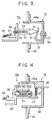
- Fig. 3 is an enlarged cross-sectional view showing a high-voltage contact section thereof.
- a photosensitive drum 1 carries a toner image developed by a developing device (not shown) and, subsequently, the toner image carried on the photosensitive drum 1 is transferred to a transfer material by an operation of a transfer electrifying device 3. Furthermore, a pair of register rollers 2 convey the transfer material to the toner image on the photosensitive drum 1, and the transfer electrifying device 3 transfers the toner image on the photosensitive drum 1 onto that transfer material.
- the transfer material having thereon the toner image is separated from the photosensitive drum 1 by means of a separation rectifying device 4 and is then conveyed to a pair of fixing rollers 6 through a conveying belt 5.
- the fixing roller pair 6 fix the toner image on the transfer material, following which the transfer material is ejected to the external through the use of a pair of ejecting rollers 7.
- the register roller pair 2, the transfer electrifying device 3, the separation electrifying device 4, the conveying belt 5, the fixing roller pair 6 and the ejecting roller pair 7 are all fixed on a unit base plate 8, and are constructed as a fixing/conveying unit 9 to be attachable/detachable simultaneously to/from the main body of the image forming apparatus.
- the transfer electrifying device 3 and the separation electrifying device 4 of this fixing/conveying unit 9 are equipped with high-voltage contact sections 12a and 12b, respectively (see Fig. 1).
- the high-voltage contact sections 12a and 12b are brought into contact with a main body contact section 13 so that the transfer electrifying device 3 and the separation electrifying device 4 receive a power supply.
- the high-voltage contact section for the separation electrifying device 4 in the image forming apparatus are constructed as shown in Fig. 3.
- the high-voltage contact section for the separation electrifying device 4 in the image forming apparatus is made up of a separation electrifying device contact portion 21, a separation electrifying device block 22, a resistor 23, a connecting portion 24, a spring latching plate 25, a main body contact 31, a main body contact block 32, a base plate contact 33 and a main body frame 40.
- the high-voltage contact section 12b of the separation electrifying device 4 is constructed with the separation electrifying device contact portion 21, the resistor 23 and the connecting portion 24 embedded in the separation electrifying device block 22, and the separation electrifying device contact portion 21, the resistor 23 and the connecting portion 24 are connected electrically to each other. Additionally, the spring latching plate 25 is attached through a screw 27 to the connecting portion 24. Incidentally, it is also appropriate that the connecting portion 24 and the spring latching plate 25 are constructed as an integrated unit.
- an electrifying wire (not shown) is attached through a spring 26 to the spring latching plate 25 to establish an electrical connection.
- the main body contact 31 made from a metallic elastic material and the base plate contact 33 are attached to the main body contact block 32, with the main body contact 31 and the base plate contact 33 connected electrically to each other.
- the base plate contact 33 is also connected to a main body high-voltage base plate (not shown), while the main body contact block 32 is fit into an opening portion 40a, made in a rear surface of the main body frame 40, to be set thereat.
- the separation electrifying device contact portion 21 is inserted into the opening portion 40a made in the rear surface of the main body frame 40 and is brought into contact with the main body contact 31, situated on the rear surface of the main body frame 40, to establish electrical connection between separation electrifying device contact portion 21 and main body contact 31.
- a high AC voltage generated from a main body pressing base plate (not shown) is supplied to the base plate contact 33, the main body contact 31 and the separation electrifying device contact portion 21 in this order so that the electrifying wire (not shown) performs the corona discharge, that is, conducts the transfer material separating operation.
- the separation electrifying device contact portion 21 is formed into a conical configuration.
- the reason for a conical configuration is that when the fixing/conveying unit 9 is mounted in the image forming apparatus in a state where the transfer material is left in error after a jam handling operation or the like, there is the possibility of a fire if the transfer material is put between the separation electrifying device contact portion 21 and the main body contact 31. Accordingly, to prevent this, the separation electrifying device contact portion 21 is made pointed so as to break through the transfer material and, further, to come into contact with the main body contact 31 for securing the electrical connection.
- the separation electrifying device 4 conducts the separating operation, a radiation noise occurs in the high-voltage contact section and, if the right-hand area of the main body frame 40 is designed to be exterior of the apparatus, then this creates an apparatus radiation noise problem.
- the resistor 23 is placed in the left-hand area (the front side of the opening portion 40a of the main body frame 40) with respect to the vicinity of the main body frame 40 and the power load such as the corona discharge is disposed downstream, which reduces the radiation noise occurring in the high-voltage contact section so that the radiation noise occurring on the right side of the main body frame 40 is reduced. That reduction effect was as much as 10 dB or more, and it was confirmed that this arrangement functions sufficiently as a countermeasure against the radiation noise.
- Fig. 4 is an enlarged cross-sectional view showing a high-voltage contact section for a separation electrifying device 4 in an image forming apparatus according to this embodiment.
- the high-voltage contact section 12b for the separation electrifying device 4 in the image forming apparatus is composed df a separation electrifying device contact portion 21', a separation electrifying device block 22', a resistor 23, a connecting portion 24', a spring latching plate 25, a main body contact 31', a main body contact block 32', a base plate contact 33' and a main body frame 40.
- the separation electrifying device contact portion 21' and the spring latching plate 25 are fit through the connecting portion 24' to the separation electrifying device block 22'.
- the connecting portion 24' is constructed such that metallic pins 24'a and 24'b are connected to the resistor 23 and a mold 24'c is put around them to form a cylindrically embedded configuration.
- the separation electrifying device contact portion 21', the resistor 23 and the spring latching plate 25 are connected electrically to each other, and an electrifying wire (not shown) is attached through a spring 26 to the spring latching plate 25 to establish electrical connection.
- the main body contact 31' made from a metallic elastic material is attached to the base plate contact 33', and the base plate contact 33' is attached to the main body contact block 32'.
- the main body contact 31' and the base plate contact 33' are connected electrically to each other, while the base plate contact 33' is connected to a main body high-voltage base plate (not shown).
- the main body contact block 32' is fitted in an opening portion 40a, made in a rear surface of the main body frame 40, to be set thereat.
- the separation electrifying device contact portion 21' is inserted into the opening portion 40a made in the rear surface of the main body frame 40 and is brought into contact with the main body contact 31' situated on the rear surface of the main body frame 40 to establish an electrical connection therebetween.
- a high AC voltage generated from a main body pressing base plate (not shown) is supplied to the base plate contact 33', the main body contact 31' and the separation electrifying device contact portion 21' so that the electrifying wire (not shown) performs the corona discharge to conduct the transfer material separating operation.
- This embodiment is characterized in that the connecting portion 24' is made to be attachable/detachable with respect to the separation electrifying device block 32'. This is because, taking into consideration a radiation noise countermeasure in the image forming apparatus, easy changing of the resistor 23 allows a wider range of applications. The frequency of the radiation noise can vary according to the using condition of the image forming apparatus. At this time, if the resistor 23 is embedded in the separation electrifying device block 32' as well as the above-described first embodiment, the image forming apparatus requires a new mold for the separation electrifying device block 32 at every specification.
- the connecting portion 24' is detachable, when a need for changing of the type of the resistor 23 arises, the alteration can be confined to a minimum.
- this construction can flexibly cope with various specifications. Also in this embodiment, it was confirmed that sufficient effects are attainable for the reduction of radiation noise.
- a discharge device has a discharge wire for discharge in response to a voltage, a supporting block for supporting the discharge wire, an electric contact receiving an AC voltage, and a resistor element placed between the discharge wire and the electric contact.
- the discharge device serves particularly as a separation charger of an image forming apparatus.
Landscapes
- Physics & Mathematics (AREA)
- General Physics & Mathematics (AREA)
- Engineering & Computer Science (AREA)
- Plasma & Fusion (AREA)
- Electrostatic Charge, Transfer And Separation In Electrography (AREA)
- Electrophotography Configuration And Component (AREA)
Abstract
Description
Claims (18)
- A discharge device comprising:a discharging unit;a supporter member for supporting said discharging unit;an electrifying device contact portion; anda resister element placed between said discharging unit and said electrifying device contact portion.
- A discharge device according to claim 1, wherein an AC voltage is applied to said electrifying device contact portion.
- A discharge device according to claim 2, further comprising a discharge wire attached to said discharging unit.
- A discharge device according to claim 1, wherein said electrifying device contacting portion has a conical shape and is adapted for contact with a conductive elastic member.
- A discharge device according to claim 1, wherein said resistor element is attachable to and detachable from said supporting member.
- An image forming apparatus comprising:an image forming unit having a separation rectifying device;an AC base plate;a main body contact connected to said AC base plate; andan attachable/detachable high-voltage contact section for contact with said main body contact, comprising:a discharging unit;a supporter member for supporting said discharging unit;an electrifying device contact portion in contact with said main body contact; anda resistor element placed between said discharging unit and said electrifying device contact portion.
- An image forming apparatus according to claim 6, further comprising a frame installed on a rear side of a main body of said image forming apparatus, wherein said main body contact is disposed exterior to said frame.
- An image forming apparatus according to claim 7, wherein said frame has an opening portion for enabling contact of said electrifying device contact portion with said main body contact when said high-voltage contact section is mounted.
- An image forming apparatus according to claim 7, wherein said resistor element is disposed interior of said frame.
- An image forming apparatus according to claim 6, wherein the AC voltage is applied to the separation rectifying device thru a discharge wire.
- An image forming apparatus according to claim 6, wherein said main body contact is a conductive elastic member.
- An image forming apparatus according to claim 6, wherein said resistor element is attachable to and detachable from said supporter member.
- An image forming apparatus according to claim 6, wherein said image forming unit comprises an image carrier for carrying a toner image and transfer means for transferring said toner image on said image carrier to a transfer material, with said high-voltage contact section conducts electrification elimination of said transfer material after the transferring.
- An image forming apparatus comprising:an image forming unit having a high-voltage component;an AC base plate;a main body contact connected to said AC base plate; andan attachable/detachable high-voltage contact section for contact with said main body contact, comprising:a discharging unit;a supporting member for supporting said discharging unit;an electrifying device contact portion in contact with said main body contact; anda resistor element placed between said discharging unit and said electrifying device contact portion.
- An image forming apparatus according to claim 14, further comprising a frame installed on a rear side of a main body of said image forming apparatus, wherein said main body contact is disposed exterior to said frame.
- An image forming apparatus according to claim 14, wherein said frame has an opening portion for enabling contact of said electrifying device contact portion with said main body contact when said high-voltage contact section is mounted.
- An image forming apparatus according to claim 14, wherein said resistor element is disposed interior of said frame.
- An image forming apparatus according to claim 14, wherein said resistor element is attachable to and detachable from said supporting member.
Applications Claiming Priority (2)
| Application Number | Priority Date | Filing Date | Title |
|---|---|---|---|
| JP17104599 | 1999-06-17 | ||
| JP11171045A JP2001005257A (en) | 1999-06-17 | 1999-06-17 | Charging device and image forming device |
Publications (3)
| Publication Number | Publication Date |
|---|---|
| EP1061421A2 true EP1061421A2 (en) | 2000-12-20 |
| EP1061421A3 EP1061421A3 (en) | 2002-12-11 |
| EP1061421B1 EP1061421B1 (en) | 2007-10-10 |
Family
ID=15916074
Family Applications (1)
| Application Number | Title | Priority Date | Filing Date |
|---|---|---|---|
| EP00112686A Expired - Lifetime EP1061421B1 (en) | 1999-06-17 | 2000-06-15 | Combined fixing/conveying unit with discharge device for an image forming apparatus |
Country Status (6)
| Country | Link |
|---|---|
| US (1) | US6411794B1 (en) |
| EP (1) | EP1061421B1 (en) |
| JP (1) | JP2001005257A (en) |
| KR (1) | KR100335732B1 (en) |
| CN (1) | CN1222838C (en) |
| DE (1) | DE60036664T2 (en) |
Families Citing this family (3)
| Publication number | Priority date | Publication date | Assignee | Title |
|---|---|---|---|---|
| JP4359854B2 (en) * | 2007-01-30 | 2009-11-11 | ブラザー工業株式会社 | Process unit and image forming apparatus |
| JP5644391B2 (en) * | 2010-11-09 | 2014-12-24 | 富士ゼロックス株式会社 | Electrical connection structure, image forming apparatus |
| CN116859697B (en) | 2023-07-10 | 2026-02-06 | 珠海奔图电子有限公司 | Adapter, cartridge set, and image forming apparatus |
Family Cites Families (8)
| Publication number | Priority date | Publication date | Assignee | Title |
|---|---|---|---|---|
| US2863063A (en) * | 1955-11-21 | 1958-12-02 | Bruning Charles Co Inc | Charging of photo-conductive insulating material |
| JPS5519727A (en) * | 1978-07-27 | 1980-02-12 | Canon Kk | High voltage power supply device |
| JPS58126544A (en) * | 1981-12-23 | 1983-07-28 | Toshiba Corp | Corona discharger of image forming device |
| JPS59102258A (en) * | 1982-12-06 | 1984-06-13 | Canon Inc | Corona discharger |
| GB2139428B (en) * | 1983-05-02 | 1987-10-28 | Xerox Corp | Corona generating apparatus |
| JP2665290B2 (en) * | 1992-01-31 | 1997-10-22 | 三田工業株式会社 | Separation device |
| DE4305686C2 (en) * | 1992-02-24 | 1999-07-15 | Fujitsu Ltd | Toner image transfer device including a transfer charger and an AC charge eraser |
| US5815771A (en) * | 1997-04-11 | 1998-09-29 | Xerox Corporation | Apparatus for applying a high voltage electrical point of load contact |
-
1999
- 1999-06-17 JP JP11171045A patent/JP2001005257A/en active Pending
-
2000
- 2000-06-15 US US09/594,558 patent/US6411794B1/en not_active Expired - Fee Related
- 2000-06-15 DE DE60036664T patent/DE60036664T2/en not_active Expired - Lifetime
- 2000-06-15 EP EP00112686A patent/EP1061421B1/en not_active Expired - Lifetime
- 2000-06-16 CN CNB001216430A patent/CN1222838C/en not_active Expired - Fee Related
- 2000-06-17 KR KR1020000033409A patent/KR100335732B1/en not_active Expired - Fee Related
Also Published As
| Publication number | Publication date |
|---|---|
| KR100335732B1 (en) | 2002-05-09 |
| EP1061421B1 (en) | 2007-10-10 |
| DE60036664T2 (en) | 2008-07-17 |
| JP2001005257A (en) | 2001-01-12 |
| DE60036664D1 (en) | 2007-11-22 |
| CN1280318A (en) | 2001-01-17 |
| US6411794B1 (en) | 2002-06-25 |
| EP1061421A3 (en) | 2002-12-11 |
| CN1222838C (en) | 2005-10-12 |
| KR20010021001A (en) | 2001-03-15 |
Similar Documents
| Publication | Publication Date | Title |
|---|---|---|
| EP1016939A3 (en) | Image developing apparatus, process cartridge, electrophotographic image forming apparatus, and development unit frame | |
| CN120266064A (en) | A processing box | |
| CN100489690C (en) | Image forming apparatus | |
| US6411794B1 (en) | Discharge device and image forming apparatus | |
| EP0871077B1 (en) | Printing machine with an electrical connection | |
| US10838346B2 (en) | Image forming apparatus | |
| JP2007304447A (en) | Conducting mechanism and conducting member for image forming apparatus | |
| US20180052418A1 (en) | Image forming apparatus | |
| JP5090982B2 (en) | Image forming apparatus | |
| JP3200945B2 (en) | Image forming device | |
| JP4926540B2 (en) | Image forming apparatus | |
| JP2672658B2 (en) | Transfer device | |
| JP2000010457A (en) | Image forming device | |
| JP2005274669A (en) | Image forming apparatus | |
| EP0867300B1 (en) | An image forming apparatus | |
| KR200157541Y1 (en) | Image forming apparatus of electrophotographic processor | |
| JPH0553390A (en) | Image forming device | |
| JP3222565B2 (en) | Image forming device | |
| JP6987512B2 (en) | Image forming device | |
| JPH0863077A (en) | Image forming device | |
| JP2023142277A (en) | Image forming device | |
| CN106200292B (en) | Attachment device and image forming apparatus | |
| JPS6180168A (en) | Destaticizing device | |
| JP2020126105A (en) | Image forming device | |
| JPH1152655A (en) | Image forming device |
Legal Events
| Date | Code | Title | Description |
|---|---|---|---|
| PUAI | Public reference made under article 153(3) epc to a published international application that has entered the european phase |
Free format text: ORIGINAL CODE: 0009012 |
|
| AK | Designated contracting states |
Kind code of ref document: A2 Designated state(s): AT BE CH CY DE DK ES FI FR GB GR IE IT LI LU MC NL PT SE |
|
| AX | Request for extension of the european patent |
Free format text: AL;LT;LV;MK;RO;SI |
|
| PUAL | Search report despatched |
Free format text: ORIGINAL CODE: 0009013 |
|
| AK | Designated contracting states |
Kind code of ref document: A3 Designated state(s): AT BE CH CY DE DK ES FI FR GB GR IE IT LI LU MC NL PT SE |
|
| AX | Request for extension of the european patent |
Free format text: AL;LT;LV;MK;RO;SI |
|
| 17P | Request for examination filed |
Effective date: 20030423 |
|
| AKX | Designation fees paid |
Designated state(s): DE FR GB IT |
|
| 17Q | First examination report despatched |
Effective date: 20041015 |
|
| GRAP | Despatch of communication of intention to grant a patent |
Free format text: ORIGINAL CODE: EPIDOSNIGR1 |
|
| 17Q | First examination report despatched |
Effective date: 20041015 |
|
| RIC1 | Information provided on ipc code assigned before grant |
Ipc: G03G 21/16 20060101ALI20070212BHEP Ipc: G03G 15/00 20060101AFI20070212BHEP |
|
| RTI1 | Title (correction) |
Free format text: COMBINED FIXING/CONVEYING UNIT WITH DISCHARGE DEVICE FOR AN IMAGE FORMING APPARATUS |
|
| GRAS | Grant fee paid |
Free format text: ORIGINAL CODE: EPIDOSNIGR3 |
|
| GRAA | (expected) grant |
Free format text: ORIGINAL CODE: 0009210 |
|
| AK | Designated contracting states |
Kind code of ref document: B1 Designated state(s): DE FR GB IT |
|
| REG | Reference to a national code |
Ref country code: GB Ref legal event code: FG4D |
|
| REF | Corresponds to: |
Ref document number: 60036664 Country of ref document: DE Date of ref document: 20071122 Kind code of ref document: P |
|
| EN | Fr: translation not filed | ||
| PLBE | No opposition filed within time limit |
Free format text: ORIGINAL CODE: 0009261 |
|
| STAA | Information on the status of an ep patent application or granted ep patent |
Free format text: STATUS: NO OPPOSITION FILED WITHIN TIME LIMIT |
|
| 26N | No opposition filed |
Effective date: 20080711 |
|
| PG25 | Lapsed in a contracting state [announced via postgrant information from national office to epo] |
Ref country code: FR Free format text: LAPSE BECAUSE OF FAILURE TO SUBMIT A TRANSLATION OF THE DESCRIPTION OR TO PAY THE FEE WITHIN THE PRESCRIBED TIME-LIMIT Effective date: 20080725 |
|
| GBPC | Gb: european patent ceased through non-payment of renewal fee |
Effective date: 20080615 |
|
| PG25 | Lapsed in a contracting state [announced via postgrant information from national office to epo] |
Ref country code: GB Free format text: LAPSE BECAUSE OF NON-PAYMENT OF DUE FEES Effective date: 20080615 |
|
| PG25 | Lapsed in a contracting state [announced via postgrant information from national office to epo] |
Ref country code: IT Free format text: LAPSE BECAUSE OF NON-PAYMENT OF DUE FEES Effective date: 20080630 |
|
| PGFP | Annual fee paid to national office [announced via postgrant information from national office to epo] |
Ref country code: DE Payment date: 20130630 Year of fee payment: 14 |
|
| REG | Reference to a national code |
Ref country code: DE Ref legal event code: R119 Ref document number: 60036664 Country of ref document: DE |
|
| REG | Reference to a national code |
Ref country code: DE Ref legal event code: R119 Ref document number: 60036664 Country of ref document: DE Effective date: 20150101 |
|
| PG25 | Lapsed in a contracting state [announced via postgrant information from national office to epo] |
Ref country code: DE Free format text: LAPSE BECAUSE OF NON-PAYMENT OF DUE FEES Effective date: 20150101 |