EP1061406A2 - A polarization independent light switching device based on liquid crystal - Google Patents
A polarization independent light switching device based on liquid crystal Download PDFInfo
- Publication number
- EP1061406A2 EP1061406A2 EP00111581A EP00111581A EP1061406A2 EP 1061406 A2 EP1061406 A2 EP 1061406A2 EP 00111581 A EP00111581 A EP 00111581A EP 00111581 A EP00111581 A EP 00111581A EP 1061406 A2 EP1061406 A2 EP 1061406A2
- Authority
- EP
- European Patent Office
- Prior art keywords
- light signal
- light
- polarization
- waveguide
- liquid crystal
- Prior art date
- Legal status (The legal status is an assumption and is not a legal conclusion. Google has not performed a legal analysis and makes no representation as to the accuracy of the status listed.)
- Granted
Links
- 230000010287 polarization Effects 0.000 title claims abstract description 48
- 239000004973 liquid crystal related substance Substances 0.000 title claims description 44
- 230000005684 electric field Effects 0.000 claims description 14
- 239000013078 crystal Substances 0.000 claims description 11
- 239000000463 material Substances 0.000 claims description 10
- 230000001419 dependent effect Effects 0.000 claims description 3
- 230000000903 blocking effect Effects 0.000 abstract description 2
- 239000000835 fiber Substances 0.000 description 25
- 230000003287 optical effect Effects 0.000 description 11
- 238000000034 method Methods 0.000 description 3
- 230000005540 biological transmission Effects 0.000 description 2
- 230000008859 change Effects 0.000 description 2
- 238000003491 array Methods 0.000 description 1
- 238000006243 chemical reaction Methods 0.000 description 1
- 239000011248 coating agent Substances 0.000 description 1
- 238000000576 coating method Methods 0.000 description 1
- 238000004891 communication Methods 0.000 description 1
- 230000008878 coupling Effects 0.000 description 1
- 238000010168 coupling process Methods 0.000 description 1
- 238000005859 coupling reaction Methods 0.000 description 1
- 230000003993 interaction Effects 0.000 description 1
- 150000002500 ions Chemical class 0.000 description 1
- 238000012986 modification Methods 0.000 description 1
- 230000004048 modification Effects 0.000 description 1
- 230000008569 process Effects 0.000 description 1
- 238000009736 wetting Methods 0.000 description 1
Images

Classifications
-
- G—PHYSICS
- G02—OPTICS
- G02F—OPTICAL DEVICES OR ARRANGEMENTS FOR THE CONTROL OF LIGHT BY MODIFICATION OF THE OPTICAL PROPERTIES OF THE MEDIA OF THE ELEMENTS INVOLVED THEREIN; NON-LINEAR OPTICS; FREQUENCY-CHANGING OF LIGHT; OPTICAL LOGIC ELEMENTS; OPTICAL ANALOGUE/DIGITAL CONVERTERS
- G02F1/00—Devices or arrangements for the control of the intensity, colour, phase, polarisation or direction of light arriving from an independent light source, e.g. switching, gating or modulating; Non-linear optics
- G02F1/01—Devices or arrangements for the control of the intensity, colour, phase, polarisation or direction of light arriving from an independent light source, e.g. switching, gating or modulating; Non-linear optics for the control of the intensity, phase, polarisation or colour
- G02F1/13—Devices or arrangements for the control of the intensity, colour, phase, polarisation or direction of light arriving from an independent light source, e.g. switching, gating or modulating; Non-linear optics for the control of the intensity, phase, polarisation or colour based on liquid crystals, e.g. single liquid crystal display cells
- G02F1/1326—Liquid crystal optical waveguides or liquid crystal cells specially adapted for gating or modulating between optical waveguides
-
- G—PHYSICS
- G02—OPTICS
- G02F—OPTICAL DEVICES OR ARRANGEMENTS FOR THE CONTROL OF LIGHT BY MODIFICATION OF THE OPTICAL PROPERTIES OF THE MEDIA OF THE ELEMENTS INVOLVED THEREIN; NON-LINEAR OPTICS; FREQUENCY-CHANGING OF LIGHT; OPTICAL LOGIC ELEMENTS; OPTICAL ANALOGUE/DIGITAL CONVERTERS
- G02F1/00—Devices or arrangements for the control of the intensity, colour, phase, polarisation or direction of light arriving from an independent light source, e.g. switching, gating or modulating; Non-linear optics
- G02F1/01—Devices or arrangements for the control of the intensity, colour, phase, polarisation or direction of light arriving from an independent light source, e.g. switching, gating or modulating; Non-linear optics for the control of the intensity, phase, polarisation or colour
- G02F1/21—Devices or arrangements for the control of the intensity, colour, phase, polarisation or direction of light arriving from an independent light source, e.g. switching, gating or modulating; Non-linear optics for the control of the intensity, phase, polarisation or colour by interference
-
- G—PHYSICS
- G02—OPTICS
- G02F—OPTICAL DEVICES OR ARRANGEMENTS FOR THE CONTROL OF LIGHT BY MODIFICATION OF THE OPTICAL PROPERTIES OF THE MEDIA OF THE ELEMENTS INVOLVED THEREIN; NON-LINEAR OPTICS; FREQUENCY-CHANGING OF LIGHT; OPTICAL LOGIC ELEMENTS; OPTICAL ANALOGUE/DIGITAL CONVERTERS
- G02F2203/00—Function characteristic
- G02F2203/06—Polarisation independent
Definitions
- the present invention relates to light guides, and more particularly, to programmable light guides based on liquid crystals.
- Data communication systems based on fiber optics provide substantially higher bandwidth than systems based on electrical systems.
- switching devices for switching optical signals between an input fiber and a plurality of output fibers have not kept pace.
- optical signals are typically converted back to electrical signals prior to switching.
- the electrical signals are then switched using conventional packet switching techniques and reconverted to optical signals prior to entering the output fibers.
- the limitations of electrical switching systems prevent the realization of the full data bandwidth of the fibers. Accordingly, a significant amount of research has gone into developing optical switches that avoid the conversion of the light signals back to electrical signals.
- a waveguide may be generated by altering the index of refraction of a medium along the path over which the light is to travel such that the desired path has a higher index of refraction than the surrounding medium.
- Devices based on liquid crystals are particularly attractive because of the large changes in index of refraction that can be induced in a liquid crystal layer by applying a low frequency AC electrical field across the layer.
- a simple switching device can be constructed by energizing one set of electrodes on the surface of the liquid crystal layer while leaving an alternative set in a non-energized state. The region between the energized electrodes then becomes the waveguide that specifies the direction in which the light signal will propagate in the liquid crystal layer.
- liquid crystal based light guides only guide light of one linear polarization.
- Light of the orthogonal polarization experiences a different index of refraction and is not guided. Since optical signals in such systems typically have randomly changing polarization states, unpredictable transmission can occur.
- the present invention is a light guiding element for routing a light signal between an input port and an output port or for blocking the propagation of the light signal between the input and output ports depending on the state of the light guiding element.
- the light guiding element utilizes a polarizing beam splitter for separating the input light signal into physically separated first and second polarized light signals, the first light signal having a polarization that is orthogonal to that of the second light signal.
- a first polarization rotator rotates the polarization of the first light signal such that the polarization of the first light signal is parallel to that of the second light signal.
- a first waveguide having first and second states operates on the first light signal such that the first waveguide guides the first light signal along a predetermined path in the first state while not guiding the first light signal in the second state.
- a second waveguide having first and second states operates on the second light signal such that the second waveguide guides the second light signal along a predetermined path in the first state while not guiding the second light in the second state.
- a second polarization rotator rotates the polarization of the second light signal such that the polarization of the second light signal is orthogonal to that of the first light signal.
- a polarizing beam combiner then combines the first and second light signals and couples the same to the output light port.
- the first and second waveguides are preferably constructed from a guide layer of a guide material having a first index of refraction in the absence of an electric field and a second index of refraction in the presence of an electric field.
- First and second electrodes apply the electric field to a portion of the layer.
- the electrodes define a guide region in the layer having an index of refraction that is greater than that of the guide layer in regions adjacent to the guide region.
- the guide material is preferably a liquid crystal medium.
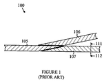
- FIG. 1 is a top view of a prior art switching device 100 for switching light signals from an input waveguide defined by an electrode 105 to either waveguide of two output waveguides defined by electrodes 106 and 107.
- the electrodes are placed on one surface of a liquid crystal layer.
- Corresponding electrodes are placed on the other side of the liquid crystal layer.
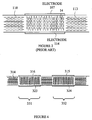
- the placement of the electrodes may be more easily understood with reference to Figure 2, which is a cross sectional view of the switching arrangement shown in Figure 1 through line 111-112.
- the liquid crystal waveguide operates by creating a region under an energized electrode in which the index of refraction is greater than that in the surrounding liquid crystal medium.
- An AC field is applied across a portion of a liquid crystal layer 110 to change the orientation of the liquid crystal molecules in the applied field as shown at 14. Coupling an appropriate signal generator between electrodes 107 and 114 generates this field.
- a liquid crystal alignment layer is applied to the walls of the chamber that causes the crystals to be aligned as shown at 113 in the absence of an electric field. When an electric field is applied, the liquid crystals that are not in contact with the crystals on the walls are re-oriented to the direction of the electric field. When the field is removed, the liquid crystals reorient themselves with the crystals in contact with the walls of the chamber.
- An AC field is utilized to switch the direction of orientation because a DC field would result in ions within the liquid crystals drifting toward one of the electrodes over time.
- the walls of the chamber can be textured such that the molecules of the liquid crystal will assume a specific orientation at the wall.
- the wall surface can be coated with a material that is then textured by rubbing to produce small grooves.
- the liquid crystal molecules will align themselves in the grooves provided the material is chosen such that the liquid crystals will wet the wall surface. If a non-wetting coating material is utilized, the liquid crystal molecules will align themselves perpendicular to the wall to minimize the interactions with the wall.
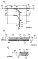
- FIG. 3 is a top view of a light switch 300 according to the present invention.
- Figure 4 is a cross-sectional view of the portion of switch 300 through line 321-322.
- Light switch 300 transmits light between input fiber 301 and output fiber 302 in one state and blocks the transmission of light between the fibers when the switch is in the other state.
- the input light signal is first separated into two polarized light beams 308 and 309 having orthogonal polarizations by walk-off crystal 310.
- walk-off crystal 310 walk-off crystal 310.
- the polarization of light beam 308 is perpendicular to the drawing sheet.
- the polarization of light beam 309 is rotated through 90 degrees by beam rotator 312. At this point, the two light beams 308 and 309, both have the same polarization direction.
- the two light beams enter a pair of switchable waveguides such as those described above.
- the waveguides are constructed from a single liquid crystal layer 314.
- the top electrodes of the waveguides are shown at 315 and 316. When an AC field is applied across these electrodes and the corresponding bottom electrodes 323 and 324, the light beams are guided in the liquid crystal layer. When no such field is present, the light beams are dispersed and the signals lost.
- the light signal on path 308 is rotated through 90 degrees by polarization rotator 317.
- the two light beams are then recombined in walk-off crystal 318.
- paths traversed by the two separated polarization beams are preferably the same. This arrangement avoids the introduction of phase differences between the light signals. In the embodiment shown in Figures 3 and 4, this is accomplished by rotating each beam through 90° and requiring each beam to traverse paths in which the beam "walks-off" in one walk-off crystal and does not walk-off in the other. Hence, each beam traverses a path that is identical in length and optical materials as that traversed by the other beam.
- the above-described embodiment of the present invention utilizes walk-off crystals to separate the incoming light into two polarized beams having orthogonal polarizations.
- other optical elements that split a beam into two component beams having orthogonal polarizations may be utilized for this purpose.
- a polarization dependent beam splitter constructed from a material that reflects one polarization while passing the other may be utilized to separate the light signal into two beams.
- the above-described embodiments of the present invention utilize beam rotators that are separate from the liquid crystal layer.
- Such rotators may be constructed from half wave plates.
- the beam rotators can be implemented by using the liquid crystal boundary layers at the input and output of the waveguides. For example, if the entry window of the beam to be rotated has an orientation layer that is parallel to the direction of polarization of the input light beam, then a region of gradual change in liquid crystal orientation will be created between the entrance window and the remainder of the liquid crystal layer. This region will rotate the incoming polarization vector of the light to match the desired polarization within the waveguide. This same process can be used for rotating the polarization angle of the light beam as it leaves the exit window.
- FIG. 5-7 illustrate a cross-connect switch 400.
- Figure 5 is a top view of switch 400.
- Figures 6 and 7 are cross-sectional views of switch 400 through lines 443-444 and 441-442, respectively.
- Switch 400 routes light signals from input fibers 401 and 402 to output fibers 411, 412, and 419.
- Switch 400 is constructed on two liquid crystal layers shown at 421 and 422. The manner in which switch 400 operates will be explained in terms of the routing of signals from input fiber 401 to either output fiber 411 or output fiber 419.
- the routing is accomplished by creating waveguides in each of the liquid crystal layers.
- the waveguides are created by applying signals to electrodes on the surface of the liquid crystal layers.
- the electrode pattern on liquid crystal layer 421 is shown in Figure 5.
- Liquid crystal layer 422 has an identical pattern. Liquid crystal layer 421 routes the portion of the light signal having one polarization, and liquid crystal layer 422 routes the portion of the light signal having the orthogonal polarization.
- the input light signal is separated into the two orthogonal components by walk-off crystal 404 which routes one of the components to liquid crystal layer 421 and the other to liquid crystal layer 422.
- the component routed to liquid crystal layer 422 is rotated through 90° by half wave plate 405 in a manner analogous to that described above.
- electrode 409 and the corresponding electrode on layer 422 are energized. In this configuration, electrode 431 and the corresponding electrode on layer 422 remain unenergized. This creates two waveguides, one in each layer, connecting fiber 401 to fiber 411. The signals from the two waveguides are recombined by walk-off crystal 407 after the signal in layer 421 is rotated through 90° by half wave plate 406.
- electrode 409 and the corresponding electrode on layer 422 remain unenergized.
- electrodes 431, 433, 415 and the corresponding electrode on layer 422 are energized. This creates two waveguides, one in each layer, connecting fiber 401 to fiber 419.
- the signals from the two waveguides are recombined by walk-off crystal 417 after the signal in layer 421 is rotated through 90° by half wave plate 416.
- switch 400 is only a 2x1 cross-connect, it will be obvious to those skilled in the art from the preceding discussion that the present invention may be utilized to construct a general NxM cross-connect switch.
Landscapes
- Physics & Mathematics (AREA)
- Nonlinear Science (AREA)
- General Physics & Mathematics (AREA)
- Optics & Photonics (AREA)
- Chemical & Material Sciences (AREA)
- Crystallography & Structural Chemistry (AREA)
- Liquid Crystal (AREA)
- Optical Modulation, Optical Deflection, Nonlinear Optics, Optical Demodulation, Optical Logic Elements (AREA)
Abstract
Description
Claims (7)
- A light guiding element(300)comprising: an input port(301) for receiving an input light signal; a beam splitter(310) for separating said input light signal into physically separated first and second polarized light signals, said first light signal having a polarization that is orthogonal to that of said second light signal; a first polarization rotator(309) for rotating said polarization of said first light signal such that said polarization of said first light signal is parallel to that of said second light signal; a first waveguide(331) having first and second states, said first waveguide(331) guiding said first light signal along a predetermined path in said first state while not guiding said first light signal in said second state; a second waveguide(332) having first and second states, said second waveguide(332) guiding said second light signal along a predetermined path in said first state while not guiding said second light in said second state; a second polarization rotator(317) for rotating said polarization of said first light signal such that said polarization of said first light signal is orthogonal to that of said second light signal; and a beam combiner(318) for combining said first and second light signals.
- The light guiding element(300) of Claim 1 wherein said first waveguide(331) comprises: a first guide layer(314, 421) of a guide material having a first index of refraction in the absence of an electric field and a second index of refraction in the presence of said electric field; and first and second electrodes(316, 323) for applying said electric field to a first portion of said first guide layer(314, 421), said electrodes defining a first guide region in said first guide layer(314, 421) having an index of refraction that is greater than that of said first guide layer(314, 421) in regions adjacent to said first guide region.
- The light guiding element(300) of Claim 2 wherein said second waveguide(332) comprises third and fourth electrodes(315, 324) for applying said electric field to a second portion of said first guide layer(314,421).
- The light guiding element(300) of Claim 2 or 3 wherein said second waveguide(332) comprises:a second guide layer of a guide material having a first index of refraction in the absence of an electric field and a second index of refraction in the presence of said electric field; and third and fourth electrodes for applying said electric field to a portion of said second guide layer, said electrodes defining a second guide region in said second layer having an index of refraction that is greater than that of said second guide layer in regions adjacent to said second guide region.
- The light guiding element of one of Claims 2-4 wherein said guide material comprises liquid crystals.
- The light guiding element(300) of one of the preceding Claims wherein said beam splitter(310) comprises a walk-off crystal.
- The light guiding element(300) of one of the preceding Claims wherein said beam splitter(310) comprises a polarization dependent beam splitter(310).
Applications Claiming Priority (2)
| Application Number | Priority Date | Filing Date | Title |
|---|---|---|---|
| US334483 | 1989-04-07 | ||
| US09/334,483 US6208774B1 (en) | 1999-06-16 | 1999-06-16 | Polarization independent light switching device based on liquid crystals |
Publications (3)
| Publication Number | Publication Date |
|---|---|
| EP1061406A2 true EP1061406A2 (en) | 2000-12-20 |
| EP1061406A3 EP1061406A3 (en) | 2004-01-28 |
| EP1061406B1 EP1061406B1 (en) | 2005-03-23 |
Family
ID=23307422
Family Applications (1)
| Application Number | Title | Priority Date | Filing Date |
|---|---|---|---|
| EP00111581A Expired - Lifetime EP1061406B1 (en) | 1999-06-16 | 2000-05-30 | A polarization independent light switching device based on liquid crystal waveguides |
Country Status (4)
| Country | Link |
|---|---|
| US (1) | US6208774B1 (en) |
| EP (1) | EP1061406B1 (en) |
| JP (1) | JP2001013471A (en) |
| DE (1) | DE60018849T2 (en) |
Cited By (1)
| Publication number | Priority date | Publication date | Assignee | Title |
|---|---|---|---|---|
| EP1221632A1 (en) * | 2001-01-05 | 2002-07-10 | Agilent Technologies, Inc. (a Delaware corporation) | Bistable light path device |
Families Citing this family (14)
| Publication number | Priority date | Publication date | Assignee | Title |
|---|---|---|---|---|
| US6559921B1 (en) | 1999-11-01 | 2003-05-06 | Corning Incorporated | Liquid crystal planar non-blocking NxN cross-connect |
| US6466704B1 (en) * | 2000-09-13 | 2002-10-15 | Nortel Networks (Photonics) Pty Ltd. | Optical filtering method and device |
| US6697550B2 (en) | 2001-10-24 | 2004-02-24 | Renka Corporation | Fast 1×N fiber-optic switch |
| JP4367684B2 (en) * | 2002-05-15 | 2009-11-18 | シチズンホールディングス株式会社 | Dynamic gain equalizer |
| CN1322355C (en) * | 2002-09-27 | 2007-06-20 | Jds尤尼费斯公司 | Wave length selective laser beam divider |
| US7298428B1 (en) * | 2003-01-10 | 2007-11-20 | Avanex Corporation | Liquid crystal device and method for optical performance monitoring in fiber optic communication systems |
| US20040184696A1 (en) * | 2003-03-18 | 2004-09-23 | Cheng-Hsi Miao | Integrated variable optical power splitter |
| US20060232762A1 (en) * | 2005-04-15 | 2006-10-19 | Specialty Minerals (Michigan) Inc. | Optical element, measuring apparatus and measuring method |
| US20060232763A1 (en) * | 2005-04-15 | 2006-10-19 | Specialty Minerals (Michigan) Inc. | Optical element, measuring apparatus and measuring method |
| US7259838B2 (en) * | 2005-06-17 | 2007-08-21 | Specialty Minerals (Michigan) Inc. | Optical beam separation element, measuring apparatus and method of measuring |
| US7564509B2 (en) * | 2006-07-13 | 2009-07-21 | Cairn Research Limited | Illumination of objects using spatial light modulators |
| JP5023707B2 (en) * | 2007-01-15 | 2012-09-12 | 株式会社ニコン | Tunable filter, light source device, and spectrum distribution measuring device |
| EP2157472B1 (en) * | 2007-05-31 | 2019-10-30 | Nikon Corporation | Tunable filter, light source device and spectrum distribution measuring device |
| CN109521529A (en) * | 2017-09-19 | 2019-03-26 | 香港理工大学深圳研究院 | A kind of photoswitch and optical cross connection device |
Family Cites Families (14)
| Publication number | Priority date | Publication date | Assignee | Title |
|---|---|---|---|---|
| JPS57142622A (en) * | 1981-02-27 | 1982-09-03 | Nippon Telegr & Teleph Corp <Ntt> | Photoswitch |
| JPS6138934A (en) * | 1984-07-30 | 1986-02-25 | Yamaichi Electric Mfg Co Ltd | Optical path switch |
| JPH01136116A (en) * | 1987-11-24 | 1989-05-29 | Nec Corp | Variable wavelength filter |
| US5251058A (en) * | 1989-10-13 | 1993-10-05 | Xerox Corporation | Multiple beam exposure control |
| US5044712A (en) * | 1990-06-29 | 1991-09-03 | The United States Of America As Represented By The Secretary Of The Air Force | Waveguided electrooptic switches using ferroelectric liquid crystals |
| JPH05323265A (en) * | 1992-05-25 | 1993-12-07 | Nippon Telegr & Teleph Corp <Ntt> | Polarization-independent tunable filter |
| JPH06148692A (en) * | 1992-11-02 | 1994-05-27 | Nippon Telegr & Teleph Corp <Ntt> | Tunable liquid crystal optical filter |
| JP3149120B2 (en) * | 1994-06-15 | 2001-03-26 | 日本電信電話株式会社 | Tunable wavelength optical filter |
| NL1003198C2 (en) * | 1995-07-07 | 1997-11-25 | Nederland Ptt | Polarization-independent optical device. |
| JPH0961771A (en) * | 1995-08-24 | 1997-03-07 | Toshiba Corp | Polarization scrambler |
| US5724165A (en) * | 1996-07-23 | 1998-03-03 | Macro-Vision Communications, L.L.C. | Fault-tolerant optical routing switch |
| JPH10221655A (en) * | 1997-02-03 | 1998-08-21 | Yazaki Corp | Optical device, optical switch device, and control method used for these devices |
| JPH1138451A (en) * | 1997-07-16 | 1999-02-12 | Nippon Telegr & Teleph Corp <Ntt> | Thin electric field control birefringent liquid crystal device and optical waveguide type light modulation device |
| KR20010022911A (en) * | 1997-08-13 | 2001-03-26 | 리챠드 에이. 코벨 | Switchable optical components |
-
1999
- 1999-06-16 US US09/334,483 patent/US6208774B1/en not_active Expired - Lifetime
-
2000
- 2000-05-30 DE DE60018849T patent/DE60018849T2/en not_active Expired - Lifetime
- 2000-05-30 EP EP00111581A patent/EP1061406B1/en not_active Expired - Lifetime
- 2000-06-13 JP JP2000176992A patent/JP2001013471A/en not_active Ceased
Cited By (2)
| Publication number | Priority date | Publication date | Assignee | Title |
|---|---|---|---|---|
| EP1221632A1 (en) * | 2001-01-05 | 2002-07-10 | Agilent Technologies, Inc. (a Delaware corporation) | Bistable light path device |
| US6470105B2 (en) | 2001-01-05 | 2002-10-22 | Agilent Technologies, Inc. | Bistable light path device |
Also Published As
| Publication number | Publication date |
|---|---|
| DE60018849D1 (en) | 2005-04-28 |
| US6208774B1 (en) | 2001-03-27 |
| JP2001013471A (en) | 2001-01-19 |
| EP1061406A3 (en) | 2004-01-28 |
| EP1061406B1 (en) | 2005-03-23 |
| DE60018849T2 (en) | 2006-03-23 |
Similar Documents
| Publication | Publication Date | Title |
|---|---|---|
| USRE37044E1 (en) | Tunable add/drop optical filter | |
| EP1061406B1 (en) | A polarization independent light switching device based on liquid crystal waveguides | |
| US6452702B1 (en) | N×M digitally programmable optical routing switch | |
| US5946116A (en) | 1 X N digitally programmable optical routing switch | |
| US5724165A (en) | Fault-tolerant optical routing switch | |
| US4516837A (en) | Electro-optical switch for unpolarized optical signals | |
| US6807329B2 (en) | Method and device for polarization-based all-optical switching | |
| US6275312B1 (en) | Optical routing switch | |
| US20030113055A1 (en) | Solid-state optical wavelength switches | |
| EP3234690B1 (en) | Polarisation-independent, optical multiplexing and demultiplexing systems based on ferroelectric liquid crystal phase modulators for spatial mode division multiplexing and demultiplexing | |
| US8094979B2 (en) | Polarization-based optical switching | |
| US20030142262A1 (en) | Liquid crystal planar non-blocking NxN cross-connect | |
| US6091543A (en) | Apparatus for providing non-reciprocal termination of parallel like polarization modes | |
| WO2003104885A1 (en) | Method and apparatus for switching an optical beam between first and second waveguides in a semiconductor substrate layer | |
| JP3931078B2 (en) | Bistable optical waveguide device | |
| US6525848B2 (en) | Switchable interleaved optical channel separator and isolator device and optical systems utilizing same | |
| US20020118411A1 (en) | Full-duplex optical add/drop communications system utilizing central light sources | |
| US6959124B2 (en) | Liquid crystal-based electro-optical device forming, in particular, a switch | |
| US4185884A (en) | Four port optical internal reflectance switchable coupler | |
| US7263250B1 (en) | Optical switch using polarization beam splitters | |
| AU724019C (en) | Fault-tolerant optical routing switch |
Legal Events
| Date | Code | Title | Description |
|---|---|---|---|
| PUAI | Public reference made under article 153(3) epc to a published international application that has entered the european phase |
Free format text: ORIGINAL CODE: 0009012 |
|
| AK | Designated contracting states |
Kind code of ref document: A2 Designated state(s): AT BE CH CY DE DK ES FI FR GB GR IE IT LI LU MC NL PT SE |
|
| AX | Request for extension of the european patent |
Free format text: AL;LT;LV;MK;RO;SI |
|
| RAP1 | Party data changed (applicant data changed or rights of an application transferred) |
Owner name: AGILENT TECHNOLOGIES INC. |
|
| RAP1 | Party data changed (applicant data changed or rights of an application transferred) |
Owner name: AGILENT TECHNOLOGIES INC. A DELAWARE CORPORATION |
|
| RAP1 | Party data changed (applicant data changed or rights of an application transferred) |
Owner name: AGILENT TECHNOLOGIES, INC. (A DELAWARE CORPORATION |
|
| PUAL | Search report despatched |
Free format text: ORIGINAL CODE: 0009013 |
|
| AK | Designated contracting states |
Kind code of ref document: A3 Designated state(s): AT BE CH CY DE DK ES FI FR GB GR IE IT LI LU MC NL PT SE |
|
| AX | Request for extension of the european patent |
Extension state: AL LT LV MK RO SI |
|
| RIC1 | Information provided on ipc code assigned before grant |
Ipc: 7G 02F 1/1333 B Ipc: 7G 02F 1/21 A |
|
| 17P | Request for examination filed |
Effective date: 20040629 |
|
| GRAP | Despatch of communication of intention to grant a patent |
Free format text: ORIGINAL CODE: EPIDOSNIGR1 |
|
| RTI1 | Title (correction) |
Free format text: A POLARIZATION INDEPENDENT LIGHT SWITCHING DEVICE BASED ON LIQUID CRYSTAL WAVEGUIDES |
|
| AKX | Designation fees paid |
Designated state(s): DE FR GB |
|
| GRAS | Grant fee paid |
Free format text: ORIGINAL CODE: EPIDOSNIGR3 |
|
| GRAA | (expected) grant |
Free format text: ORIGINAL CODE: 0009210 |
|
| AK | Designated contracting states |
Kind code of ref document: B1 Designated state(s): DE FR GB |
|
| REG | Reference to a national code |
Ref country code: GB Ref legal event code: FG4D |
|
| REG | Reference to a national code |
Ref country code: IE Ref legal event code: FG4D |
|
| REF | Corresponds to: |
Ref document number: 60018849 Country of ref document: DE Date of ref document: 20050428 Kind code of ref document: P |
|
| PLBE | No opposition filed within time limit |
Free format text: ORIGINAL CODE: 0009261 |
|
| STAA | Information on the status of an ep patent application or granted ep patent |
Free format text: STATUS: NO OPPOSITION FILED WITHIN TIME LIMIT |
|
| ET | Fr: translation filed | ||
| 26N | No opposition filed |
Effective date: 20051227 |
|
| PGFP | Annual fee paid to national office [announced via postgrant information from national office to epo] |
Ref country code: FR Payment date: 20060517 Year of fee payment: 7 |
|
| REG | Reference to a national code |
Ref country code: GB Ref legal event code: 732E |
|
| REG | Reference to a national code |
Ref country code: FR Ref legal event code: ST Effective date: 20080131 |
|
| PG25 | Lapsed in a contracting state [announced via postgrant information from national office to epo] |
Ref country code: FR Free format text: LAPSE BECAUSE OF NON-PAYMENT OF DUE FEES Effective date: 20070531 |
|
| PGFP | Annual fee paid to national office [announced via postgrant information from national office to epo] |
Ref country code: GB Payment date: 20100329 Year of fee payment: 11 |
|
| PGFP | Annual fee paid to national office [announced via postgrant information from national office to epo] |
Ref country code: DE Payment date: 20100526 Year of fee payment: 11 |
|
| REG | Reference to a national code |
Ref country code: DE Ref legal event code: R119 Ref document number: 60018849 Country of ref document: DE |
|
| REG | Reference to a national code |
Ref country code: DE Ref legal event code: R119 Ref document number: 60018849 Country of ref document: DE |
|
| GBPC | Gb: european patent ceased through non-payment of renewal fee |
Effective date: 20110530 |
|
| PG25 | Lapsed in a contracting state [announced via postgrant information from national office to epo] |
Ref country code: GB Free format text: LAPSE BECAUSE OF NON-PAYMENT OF DUE FEES Effective date: 20110530 |
|
| PG25 | Lapsed in a contracting state [announced via postgrant information from national office to epo] |
Ref country code: DE Free format text: LAPSE BECAUSE OF NON-PAYMENT OF DUE FEES Effective date: 20111130 |