EP1059728A2 - Integrated on-board automated alignment for a low distortion amplifier - Google Patents
Integrated on-board automated alignment for a low distortion amplifier Download PDFInfo
- Publication number
- EP1059728A2 EP1059728A2 EP00304647A EP00304647A EP1059728A2 EP 1059728 A2 EP1059728 A2 EP 1059728A2 EP 00304647 A EP00304647 A EP 00304647A EP 00304647 A EP00304647 A EP 00304647A EP 1059728 A2 EP1059728 A2 EP 1059728A2
- Authority
- EP
- European Patent Office
- Prior art keywords
- circuit
- signal
- amplifier
- amplifier circuit
- output
- Prior art date
- Legal status (The legal status is an assumption and is not a legal conclusion. Google has not performed a legal analysis and makes no representation as to the accuracy of the status listed.)
- Ceased
Links
Images
Classifications
-
- H—ELECTRICITY
- H03—ELECTRONIC CIRCUITRY
- H03G—CONTROL OF AMPLIFICATION
- H03G1/00—Details of arrangements for controlling amplification
- H03G1/04—Modifications of control circuit to reduce distortion caused by control
-
- H—ELECTRICITY
- H03—ELECTRONIC CIRCUITRY
- H03F—AMPLIFIERS
- H03F1/00—Details of amplifiers with only discharge tubes, only semiconductor devices or only unspecified devices as amplifying elements
- H03F1/32—Modifications of amplifiers to reduce non-linear distortion
- H03F1/3223—Modifications of amplifiers to reduce non-linear distortion using feed-forward
- H03F1/3229—Modifications of amplifiers to reduce non-linear distortion using feed-forward using a loop for error extraction and another loop for error subtraction
-
- H—ELECTRICITY
- H03—ELECTRONIC CIRCUITRY
- H03F—AMPLIFIERS
- H03F2201/00—Indexing scheme relating to details of amplifiers with only discharge tubes, only semiconductor devices or only unspecified devices as amplifying elements covered by H03F1/00
- H03F2201/32—Indexing scheme relating to modifications of amplifiers to reduce non-linear distortion
- H03F2201/3233—Adaptive predistortion using lookup table, e.g. memory, RAM, ROM, LUT, to generate the predistortion
Definitions
- the present invention relates to the field of low distortion, high frequency amplifiers and, more particularly to an integrated on-board automated alignment circuit for low distortion, high frequency amplifiers.
- intermodulation distortion In the amplification of a multi-tone high frequency input signal, such as the signals present in a wireless communication application, undesirable intermodulation frequencies are typically produced, resulting in distortion of the output signal (i.e., the amplified input signal).
- the resulting distortion typically referred to as intermodulation distortion (IMD)
- IMD intermodulation distortion
- Recently, low distortion amplifiers capable of amplifying the multi-tone signals while substantially eliminating the intermodulation distortion of the output signal have been developed to counteract the IMD problem.
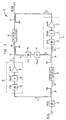
- Fig. 1 illustrates a low distortion amplifier circuit 10 capable of amplifying multi-tone input signals RF_In while substantially minimizing the intermodulation distortion of the output signal RF_Out.
- the circuit 10 contains a first amplifier circuit 30 comprising a first attenuator 32, phase shifter 34 and amplifier 36 and a second amplifier circuit 20 comprising a second attenuator 22, phase shifter 24 and amplifier 26.
- the circuit 10 also contains third and fourth attenuators 12, 44, a third phase shifter 46, four couplers 14, 18, 42, 52, and two delay circuits 16, 48.
- the input of the third attenuator 12 is connected to receive the input signal RF_In.
- the third attenuator has a control variable AttIn that can be used to adjust the overall gain of the circuit 10 (as will be described below with reference to Figs. 3a-3c).
- the output of the third attenuator 12 is connected to an input port of the first coupler 14, which is configured as a 10dB power splitter.
- the coupler 14 is typically a conventional parallel coupler line type that samples power from a direct port and a coupled port of the coupler 14.
- the direct port of the coupler 14 is connected to an input of the first delay circuit 16.
- the coupled port of the coupler 14 is connected to an input of the first attenuator 32 of the first amplifier circuit 30.
- An output of the first delay circuit 16 is connected to the input port of the second coupler 18, which is configured as a 10dB subtracting device (i.e., it subtracts signal S5 from signal S2 as described below in more detail).
- the second coupler 18 is typically a conventional parallel coupler line type coupler.
- the direct port of the coupler 18 is connected to an input of the second attenuator 22 of the second amplifier circuit 20.
- the output of the second attenuator 22 is connected to the input of the second phase shifter 24.
- the output of the second phase shifter 24 is connected to an input of the second amplifier 26.
- the amplifier 26 is typically a conventional high frequency amplifier operating in class A, AB or B and having a gain GainA on the order of 30dB to produce output power on the order of 50W.
- the output of the second amplifier 26 is connected to the coupled port of the fourth coupler 52, which is configured as a 3dB combiner.
- the fourth coupler 52 can be a conventional Wilkinson coupler with proper phase adjustment.
- the output of the first attenuator 32 is connected to the input of the first phase shifter 34.
- the output of the first phase shifter 34 is connected to the input of the first amplifier 36.
- the first amplifier 36 is typically a conventional high frequency amplifier operating in class A, AB or B and having a gain GainB on the order of 30dB to produce output power on the order of 50W.
- the output of the first amplifier 36 is connected to the input port of the third coupler 42, which is configured as a conventional 30dB splitter.
- the direct port of the third coupler 42 is connected to the input of the second delay circuit 48.
- the output of the second delay circuit 48 is connected to the direct port of the fourth coupler 52.
- the coupled port of the third coupler 42 is connected to the input of the fourth attenuator 44.
- the output of the fourth attenuator 44 is connected to the input of the third phase shifter 46.
- the output of the third phase shifter 46 is connected to the coupled port of the second coupler 18.
- an applied input signal RF_In is attenuated by the third attenuator 12 and then split into two signals S1, S2 by the first coupler 14.
- RF_In is a multi-tone high frequency signal consisting of sinusoidal components of a first fundamental frequency and a second fundamental frequency, which is higher than the first fundamental frequency. Both frequencies, however, lie within standard wireless communication frequency bands (e.g., 800Mhz to 960Mhz), although the circuit 10 can be used in other applications with lower or higher frequency bands.
- Signal S1 is applied to the first amplifier circuit 30 where it is amplified forming amplified signal S3 at the output of the first amplifier 36.
- Signal S3 will contain some undesirable intermodulation distortion products (IMD) which are in phase with the desired RF portion of the signal.
- Signal S3 is then input into third coupler 42, which outputs two signals S4, S8 representing the amplified signal S3.
- Signal S4 is attenuated by the fourth attenuator 44 and phase shifted 180 degrees by the third phase shifter 46 forming signal S5.
- Signal S5 will be 180 degrees out of phase with delayed signal S2 (described below), but with a small RE portion amplitude.
- Signal S5 is applied to the second coupler 18.
- Signal S8 is applied to the second delay circuit 48, which introduces a time delay and thus, outputs a delayed S8 to the fourth coupler 52.
- Signal S8 will contain a desirable RF portion and an undesirable IMD portion.
- Signal S2 is applied to the first delay circuit 16, which introduces a time delay and thus, outputs a delayed S2 to the second coupler 18.
- the delay ensures that the signals S2 and S5 arrive at the second coupler 18 at the same time.
- the output of the second coupler 18, signal S6, represents the subtraction of signal S5 from signal S2.
- the RF portion of S6 is approximately equal in amplitude, but 180 degrees out of phase with the RF portion of signal S1.
- S6 also contains an IMD portion from signal S5 since signal S2 does not contain IMD and no cancellation occurs.
- S6 is amplified by the second amplifier circuit 20 forming signal S7, which is applied to the fourth coupler 52.
- the IMD portion of signal S6 will be attenuated by the new IMD portion introduced by the second amplifier 26.
- signal S7 will have an IMD portion equal in amplitude, but 180 degrees out of phase with the IMD portion in signal S8.
- the RF portion of signal S7 will be in-phase with the RF portion of signal S8.
- the desired RF signal portion of the two signals S8 and S7 present at the fourth coupler 52 are in phase with each other and thus, are combined by the fourth coupler 52 to form RF_Out with a high gain (with respect to the input RF_In).
- the IMD portion of signal S8 will be equal in amplitude to the IMD portion of signal S7, but they will be 180 degrees out of phase with each other and thus, the IMD is substantially canceled. Accordingly, the circuit 10 has a large output power gain with substantially minimized intermodulation distortion.
- each attenuator 22, 32, 44 and phase shifters 24, 34, 46 must be properly balanced.
- Each attenuator 22, 32, 44 has control variables AttA, AttB, AttF, respectively, that can be set by a system user.
- each phase shifter 24, 34, 46 has control variables PhaseA, PhaseB, PhaseF, respectively, that can also be set by the system user.
- a special alignment procedure, performed off-line in a laboratory or on the production line, is necessary to find the proper setting of these variables. To speed-up production time, the alignment is typically performed at one frequency and one temperature. The obtained variables are placed into a look-up table and projected to obtain circuit performance for the remainder of the circuit's operational range.
- any alignment mechanism be integrated on-board with the amplifier so that the alignment can occur out in the field during normal operation of the amplifier, as opposed to being performed in a laboratory or at the production line. Accordingly, there is a desire and need for an integrated on-board alignment mechanism for a low distortion, high frequency amplifier.
- the present invention provides a continuous automated alignment mechanism for low distortion, high frequency amplifiers.
- the present invention also provides an integrated on-board alignment mechanism for a low distortion, high frequency amplifier.
- the above and other features and advantages of the invention are achieved by integrating a low distortion amplifier with an optimization circuit that performs an automated alignment of the amplifier.
- the optimization circuit includes an extraction circuit designed to extract various signals indicative of the operation of the amplifier under the current operating conditions.
- a control circuit using information received from the extraction circuit determines the appropriate control settings for key components of the amplifier for the current operating conditions.
- the optimization circuit ensures that the amplifier output has a desired signal level while also ensuring that the output has minimum or no intermodulation distortion under all operating conditions.
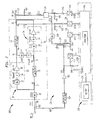
- FIG. 2 a circuit 100 for a low distortion amplifier with on-board automated alignment constructed in accordance with the present invention.
- the circuit 100 includes a modified Fig. 1 circuit denoted as 10', an indication extraction circuit 101 and a control circuit 200.
- the control circuit 200 and the extraction circuit 101 form an optimization circuit, which, as will be described below, performs an automated alignment of the amplifier circuit 10' and thus, ensures that the output RF_Out of the circuit 100 has a desired signal level while also ensuring that the output has minimum or no intermodulation distortion under all operating conditions.
- the circuit 10' is essentially the same as circuit 10 described above with reference to Fig. 1, with two minor exceptions.
- the input of third attenuator 12 is connected to a signal IN1 output from a fifth coupler 102, which is configured as a 10dB splitter and splits the input signal RF_In into two signals IN1 and IN2.
- a signal S10 output from the isolated port of the fourth coupler 52 (unused in circuit 10 of Fig. 1) is used by the extraction circuit 101 to help optimize the circuit 100 (described in detail below).
- the circuit 10' will receive a portion of the input signal IN1 and produce the desired output RF_Out with no or minimum intermodulation distortion (as described above with reference to Fig. 1).
- the extraction circuit 101 contains fifth and sixth couplers 102, 120, delay circuit 104, amplifier 106, four diodes 110, 124, 132, 142, four analog-to-digital converters (ADC) 112, 126, 134, 144, an attenuator 128, a sampling resistor 150, five shunt resistors 122, 130, 140, 152, 108 and a power divider circuit 154.
- ADC analog-to-digital converters
- the input of the fifth coupler 102 is connected to receive the input signal RF_In.
- the fifth coupler 102 is configured as a 10dB power splitter.
- the coupler 102 may be a conventional parallel coupler line type coupler.
- the direct port of the coupler 102 is connected to the input of the attenuator 12 of the amplifier circuit 10'.
- the coupled port of the fifth coupler 102 is connected to an input of the third delay circuit 104.
- the output of the delay circuit 104 is connected to the input of the third amplifier 106.
- the output of the amplifier 106 is connected to the parallel combination of the resistor 108 and the first diode 110.
- the output of the amplifier 106 is also connected to the coupled port of the sixth coupler 120, which is configured as a 3dB combiner.
- the output of diode 110 is connected to the input of ADC 112.
- the output of ADC 112 is connected to an input of the control circuit 200.
- the isolated port of the fourth coupler 52 of circuit 10' is connected to the second diode 132.
- the output of the second diode 132 is connected to the input of the second ADC 134.
- a shunt resistor 130 is also connected between a ground potential and the input of the second diode 132.
- the output of ADC 134 is connected to an input of the control circuit 200.
- the sampling resistor 150 is connected between the output port, RF_Out, of the fifth coupler 52 and the input of the power divider circuit 154.
- the sampling resistor 150 has a value that is transparent to an output transmission line.
- One exemplary value for the sampling resistor 150 would be approximately 1K Ohms.
- a shunt resistor 152 having a very small value relative to the sampling resistor 150 is connected between the sampling resistor 152 and a ground potential. If the sampling resistor 150 has a value of 1K Ohms, for example, then the shunt resistor 152 will have a value of approximately 50 Ohms.
- the power divider circuit 154 may be a simple resistor-network power divider or it may also be a 3dB coupler.
- One output of the power divider circuit 154 is connected to the input of the third diode 142.
- the output of the third diode 142 is connected to the input of the third ADC 144.
- a shunt resistor 140 is also connected between a ground potential and the input of the third diode 142.
- the output of ADC 144 is connected to an input of the control circuit 200.
- a second output of the power divider circuit 154 is connected to the input of the fifth attenuator 128.
- the output of the fifth attenuator 128 is connected to the direct port of the coupler 120.
- the input port of the coupler 120 is directly connected to the fourth diode 124.
- the output of the diode 124 is connected to the input of the fourth ADC 126.
- a shunt resistor 122 is also connected between a ground potential and the input of the fourth diode 124.
- the output of ADC 126 is connected to an input of the control circuit 200.
- the input signal RF_In is applied to the input of the fifth coupler 102 which outputs signal IN1 to the third attenuator 12 of the amplifier circuit 10' and signal IN2 to the third delay circuit 104.
- the first signal IN1 is amplified by the amplifier circuit 10', as described above with reference to Fig. 1, to obtain the desired output RF_Out.
- RF_Out is sampled by the sampling resistor 150, which when coupled with the shunt resistor 152 serves as a 22 dB attenuator and creates signal S11.
- Signal S11 is applied to the power divider circuit 154 and is split into two signals PS1 and PS2. Both PS1 and PS2 are representative of the sampled RF_Out signal.
- the PS2 output signal is applied to the third ADC 144 (via diode 142).
- the third ADC 144 digitizes the PS2 signal into signal A/D3, which is sent to the control circuit 200.
- the A/D3 signal is a digital representation of the current RF value of the output signal RF_Out of the circuit 100 and will be used by the control circuit 200 to properly set the control variables AttA, AttB, AttF, PhaseA, PhaseB, PhaseF.
- the other output of the power divider circuit 154, i.e., signal PS1 is applied to the direct port of coupler 120 (via attenuator 128), which is serving as a 3dB combiner.
- Signal IN2 which is representative of the input signal RF_In, is delayed by the third delay circuit 104 and amplified by amplifier 106 to form signal S14.
- Signal S14 is applied to the coupled port of coupler 120. Provided that the phases of the signals S14 and PS1 are correct, the signals should cancel. Any output signal S13 from the coupler 120 represents the total IMD of the amplifier circuit 10'.
- Signal S13 is applied to the fourth ADC 126 (via diode 124). The fourth ADC 126 digitizes the S13 signal into signal A/D1, which is sent to the control circuit 200.
- the A/D1 signal is a digital representation of the current value of the output IMD of the circuit 10', when the input signal RF_In is a multi-tone signal, or Spectral Regrowth if the input signal RF_In is a CDMA signal.
- A/D1 will be used by the control circuit 200 to properly set the control variables AttA, AttB, AttF, PhaseA, PhaseB, PhaseF.
- Signal S10 which is output from the isolated port of the fourth coupler 52 serves as an indication for equal gains at the first and second amplifier circuits 20, 30. That is, if both the first and second amplifier circuits 20, 30 have the same gain, then signal S10 will be at a minimum. Likewise, the signal S10 approaches a maximum value as the gains of the first and second amplifier circuits 20, 30 become increasingly unequal.
- Signal S10 is applied to the second ADC 134 (via diode 132).
- the second ADC 134 digitizes the S10 signal into signal A/D2, which is sent to the control circuit 200.
- the A/D2 signal is a digital representation of the "equal gain" indication for the first and second amplifier circuits 20, 30. As previously noted, signal A/D2 will be at a minimum when the gains are equal.
- A/D2 will be used by the control circuit 200 to properly set the control variables AttA, AttB, AttF, PhaseA, PhaseB, PhaseF.
- Signal S14 is also applied to the first ADC 112 (via diode 110).
- the first ADC 112 digitizes the S14 signal into signal A/D4, which is sent to the control circuit 200.
- the A/D4 signal is a digital representation of the current RF value of the input signal RF_In and will be used by the control circuit 200 to properly set the control variable AttIn.
- the control circuit 200 may be a processor 204 connected to or having a memory circuit 202.
- the control circuit 200 will input signals A/D1, A/D2, A/D3 and A/D4 from the extraction circuit 101 and output control signals CONTROL to set the various control variables AttIn, AttA, AttB, AttF, PhaseA, PhaseB, PhaseF of the amplifier circuit 10' so that the output of the circuit 100 has a desired signal level while also ensuring that the output contains no or minimum intermodulation distortion under all operating conditions (described below in detail with reference to Figs. 3a-3c).
- the control circuit 200 could also be implemented in hardware or an application specific integrated circuit (ASIC) or a combination of hardware and software.
- ASIC application specific integrated circuit
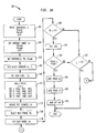
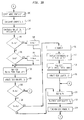
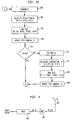
- Figs. 3a-3c illustrate in flowchart form an exemplary automated method 300 for aligning the low distortion amplifier circuit 100 having an on-board automated alignment (illustrated in Fig. 2).
- the method 300 monitors the values of the signals A/D1 (representing the output IMD) and A/D2 (representing equal gain of the first and second amplifier circuits 20, 30) to determine proper alignment of the circuit 100 (Fig. 2). Proper alignment is achieved when the signals A/D1, A/D2 are at a predetermined minimum.
- Signal A/D3 is used to adjust the output power to a fixed level to ensure that false IMD caused by insufficient output power does not occur.
- Signals A/D3 and A/D4 will eventually be used to adjust the final gain setting (via the AttIn control setting for the third attenuator 12) of the circuit 100 (Fig. 2). That is, A/D3 minus A/D4 will yield the current gain of the circuit 100, which can then be compared to a desired gain. Any adjustments needed to achieve the desired gain are made by adjusting AttIn.
- the method 300 utilize a modified simplex method technique to properly adjust the various control settings.
- the simplex method is a procedure for adjusting variables (e.g., control variable settings of circuit 100) to find settings for these variables that achieve the best possible outcome for the system (e.g., proper amplification with the gains of the first and second amplifier circuits being equal and minimum IMD in the output signal RF_Out).
- the simplex method can handle numerous variables.
- the variables may include any or all of the control variables AttA, AttB, AttF, PhaseA, PhaseB, and PhaseF.
- the simplex method begins with an initial V+1 tests or trials, where V represents the number of variables being adjusted to achieve the best possible outcome.
- V represents the number of variables being adjusted to achieve the best possible outcome.
- Each test should include different settings for at least one or any of each variable.
- the settings of each test should be sufficiently spread-out from each other so that that the initial tests encompass a large range of settings.
- the initial tests form the "simplex.”
- the individual test having the least favorable outcome is rejected and is replaced by a new test having different variable settings.
- V+1 test results there are always V+1 test results.
- the variables for the new test are calculated by a "reflection" into the original simplex, but are typically selected to be opposite to the variables leading to the undesirable outcome.
- the new test is run and a new least favorable outcome is determined and one of the V+1 tests is replaced by another new test. This procedure continues until a desired outcome is achieved. Once the desired outcome is achieved, the simplex method terminates and the variable settings resulting in the desired outcome are saved and subsequently used by the system.
- an exemplary automated method 300 for aligning the low distortion amplifier circuit 100 is shown. It is desirable that the method 300 be performed by the control circuit 200 (Fig. 2). If the control circuit 200 is implemented as a processor 204 communicating with a memory circuit 202, then the method 300 will be implemented as a software program executed by the processor 204, with the program and results of the method 300 being stored in the memory circuit 202. It should be appreciated, however, that the method 300, as well as the control circuit 200, could be implemented in hardware, ASIC or any combination of hardware and software and the method 300 of the present invention is not be limited to a microprocessor executing software. The method 300 may be run out in the field so that the circuit 100 is aligned for the current operating conditions. This way, factors such as operating temperature will be accounted for during implementation of the method 300.
- control variables PhaseA, PhaseB and AttF will be used for illustrative purposes. It should be appreciated that any combination of the control variables AttA, AttB, AttF, PhaseA, PhaseB, and PhaseF may be processed by the method 300. Control variables that are not processed by the method 300 will be set to default values based on past alignments (i.e., experience). The variables PhaseA, PhaseB and AttF will be collectively referred to herein as "V.”
- the selected control variables PhaseA, PhaseB and AttF are preset to initial values so that the circuit 100 may be operational.
- These initial values may be, for example, a mid-range value for each variable or may be some other value chosen based on past alignments (i.e., experience).
- Settings for the PhaseA and PhaseB are in degrees/volt, while settings for the AttF are in gain/volt.
- ranges for the control variables V may be set so that the method 300 selects only values within each variables range.
- the ranges for the control variables V will be collectively referred to as "Vr.”
- the desired or threshold power Pt and the desired or threshold IMD PtImd are selected.
- the threshold power Pt represents a minimum desired value for the "equal gain" of amplifiers 20 and 30 (illustrated in Fig. 2). That is, the threshold power Pt is set to a value where the gains of the first and second amplifiers 20, 30 are substantially equal.
- signal A/D2 represents the equal gain of the first and second amplifier circuits 20, 30 and will be compared to Pt to determine when the signal A/D2 is at a minimum.
- the threshold IMD PtImd is set to a value where the output IMD will be at a minimum.
- signal A/D1 represents the output IMD of the circuit 100 and will be compared to PtImd to determine when the signal A/D1 is at a minimum.
- a test counter Ct representing the number of tests performed is initialized to zero.
- a test represents loading amplifier circuit 10' (Fig. 2) to a variable set and then comparing the power values of A/D3 or A/D1 to the thresholds Pt or PtImd (described below at step 320).
- Loop counter C L is also initialized to zero.
- a number-of-loop limit Cn is set to a maximum number of test loops desired to be run by the method 300. This limit Cn prevents the method 300 from looping endlessly if the desired A/D1 and A/D2 signals are not achieved.
- the four initial tests are represented by four different sets of variables, individually labeled as set 1, set 2, set 3 and set 4.
- Set 1 includes settings PhA1, PhB1, AtF1 for the variables PhaseA, PhaseB and AttF, respectively.
- set 2 includes settings PhA2, PhB2, AtF2,
- set 3 includes settings PhA3, PhB3, AtF3 and set 4 includes settings PhA4, PhB4, AtF4.
- the test settings are collectively referred to herein as test settings PhA, PhB and AtF.
- Each test is run when the control circuit 200 sets the control variables PhaseA, PhaseB and AttF (via control signals CONTROL in Fig. 2) to the values of within one of the test sets. That is, to run the first test based on set 1, for example, PhaseA is set to PhA1, PhaseB is set to PhB1 and AttF is set to AtF1.
- the extracted signals A/D1, A/D2, A/D3, A/D4 will be indicative of the performance of the amplifier circuit 100 (Fig. 2) based on the control settings used in the test.
- the test counter Ct can be incremented (step 314).
- the current value of Ct will be V+1, or four for this example.
- the best power Pb is selected from the four sets of extracted signals (i.e., the signal A/D2 with the lowest value) and tested (i.e., compared to the threshold power Pt).
- the method 300 continues at step 324 where the extracted IMD (i.e., signal A/D1) associated with the test having the best power Pb is tested (i.e., compared to the threshold IMD Imdt).
- This extracted IMD is hereinafter referred to as PbImd.
- PbImd the extracted IMD
- the method 300 has properly aligned the low distortion amplifier circuit of the present invention. The values of the control variables used in the test are then stored away in steps 330-334 and the method 300 terminates.
- the other extracted signals A/D3 and A/D4 can be used to ensure that the circuit 100 has the desired gain. That is, A/D3 minus A/D4 will yield the current gain of the circuit 100, which can then be compared to a desired gain. Any adjustments needed to achieve the desired gain are made by adjusting AttIn of the third attenuator 12 (Fig. 2).
- step 322 determines if the method 300 should make another test loop. That is, at step 322, it is determined if the loop counter C L is greater than or equal to the loop limit Cn. If the loop counter C L is greater than or equal to the loop limit Cn, the method 300 terminates. At this point, desired output power and IMD levels have not been found and the method 300 must be re-run.
- step 340 the test set with the worst power is selected.
- This set is referred to herein as set W and will contain ⁇ W1, W2, W3 ⁇ respectively representing the test settings PhA, PhB and AtF settings resulting in the worst power.
- the method 300 performs conventional simplex method processing to replace the worst case set W with a new test set.
- a centroid set C containing ⁇ C1, C2, C3 ⁇ representing centroids for each test setting PhA, PbB and AtF used in the tests.
- C1 which represents the centroid for test setting PhA will be set to C2
- C3 which represents the centroid for test setting AtF will be set to
- a reflection set R is calculated at step 344.
- the reflection set R contains ⁇ R1, R2, R3 ⁇ .
- R1 represents the reflection for the first test setting PhA and equals C1 +(C1-W1) .
- R2 represents the reflection for the second test setting PhB and equals C2 +(C2-W2) .
- R3 represents the reflection for the third test setting AtF and equals C3 +(C3-W3) .
- the reflection R is then compared to a reflection range Vr (at step 346).
- the reflection R is set to the minimum Vmin (step 348) and the method 300 continues at step 360. If at step 346 it is determined the reflection R is greater than the minimum of reflection range Vr, the method continues at step 350 to determine if the reflection R is greater than or equal to a maximum of the range Vr. If at step 350 it is determined that the reflection R is greater than or equal to the maximum, the reflection R is set to the maximum Vmax (step 352) and the method 300 continues at step 360. If at step 350 it is determined that the reflection R is less than the maximum, the method 300 continues at step 360.
- the reflection R is used as a new test.
- the new test has a set containing PhAR, PhBR and AtFR representing the control variables PhaseA, PhaseB and AttF, respectively.
- the new test is run when the control circuit 200 sets the control variables PhaseA, PhaseB and AttF (via control signals CONTROL in Fig. 2) to the values of PhAR, PhBR and AtFR.
- the extracted signals A/D1, A/D2, A/D3, A/D4 will be indicative of the performance of the amplifier circuit 100 (Fig. 2) based on the control settings used in the new test.
- the test counter Ct can be incremented (step 364).
- the signal A/D2 associated with the reflection R test, Pr is compared to the worst case power Pw. If at step 366 it is determined that the reflection power Pr is less than the worst case power Pw, the method continues at step 368 where it is determined if the reflection power Pr is "too less" (i.e., much smaller) than the worst case power Pw.
- the term "too less” refers to a difference between the reflection power Pr and the worst case power Pw that is greater than a predetermined difference threshold, which is set by based upon past alignments and experience with simplex methods. If the reflection power Pr is too less than the worst case power Pw, the reflection will be discarded and thus, the method 300 continues at step 410. If at step 368 it is determined that the reflection power Pr is not too less than the worst case power Pw, the method 300 continues at step 370. At this point, the reflection test set R replaces the worst case set W and becomes part of the V+1 tests.
- the old worst case power Pw is set to the current reflection or new test power Pr.
- the test counter Ct is incremented (step 372) and a new best power Pb is determined from the V+1 tests (374). Once a new best power Pb is determined, the method 300 continues at step 318, where it will be tested (i.e., compared to the threshold power Pt as described above).
- the method 300 continues at step 410.
- the reflection R is discarded.
- an expansion set Er is calculated. Er equals C + ⁇ *(C-W) , where ⁇ equals 2.
- the expansion set Er contains ⁇ Er1, Er2, Er3 ⁇ .
- Er1 represents the expansion for the first test setting PhA and equals C1 +2*(C1-W1) .
- Er2 represents the expansion for the second test setting PhB and equals C2 +2*(C2-W2) .
- Er3 represents the expansion for the third test setting AtF and equals C3 +2*(C3-W3) .
- a step 414 the expansion Er is used as a new test.
- the new test has a set containing PhAEr, PhBEr and AtFEr representing the control variables PhaseA, PhaseB and AttF, respectively. This expansion set becomes part of the V+1 tests.
- the new test is run when the control circuit 200 sets the control variables PhaseA, PhaseB and AttF (via control signals CONTROL in Fig. 2) to the values of PhAEr, PhBEr and AtFEr.
- the extracted signals A/D1, A/D2, A/D3, A/D4 will be indicative of the performance of the amplifier circuit 100 (Fig. 2) based on the control settings used in the new test (based on PhAEr, PhBEr and AtFEr).
- test counter Ct can be incremented (step 418) and the method continues at step 370 where the old worst case power Pw is set to the expansion or new test power Pr.
- step 366 If at step 366 it is determined that the reflection power Pr is greater than the worst case power Pw, the method continues at step 380.
- step 380 the reflection R is discarded.
- step 382 a new compressed reflection Rc is calculated.
- the reflection set Rc contains ⁇ Rc1, Rc2, Rc3 ⁇ . This new reflection set Rc becomes part of the V+1 tests.
- Rc1 represents the new reflection for the first test setting PhA and equals C1 + 0.50*(C1-W1) .
- Rc2 represents the new reflection for the second test setting PhB and equals C2 +0.50*(C2- W2) .
- Rc3 represents the new reflection for the third test setting AtF and equals C3 +0.50*(C3-W3) .
- a step 384 the new reflection Rc is used as a new test.
- the new test has a set containing PhARc, PhBRc and AtFRc representing the control variables PhaseA, PhaseB and AttF, respectively.
- the new test is run when the control circuit 200 sets the control variables PhaseA, PhaseB and AttF (via control signals CONTROL in Fig. 2) to the values of PhARc, PhBRc and AtFRc.
- the extracted signals A/D1, A/D2, A/D3, A/D4 will be indicative of the performance of the amplifier circuit 100 (Fig. 2) based on the control settings used in the new test.
- the test counter Ct can be incremented (step 388).
- the signal A/D2 associated with the new reflection Rc test, Pr is compared to the worst case power Pw. If at step 390 it is determined that the new reflection power Pr is less than the worst case power Pw, the method continues at step 370 where the old worst case power Pw is set to the expansion or new test power Pr.
- a contraction set Cr is calculated. Cr equals C + ⁇ *(C-W) , where ⁇ equals -0.50.
- the contraction set Cr contains ⁇ Cr1, Cr2, Cr3 ⁇ .
- Cr1 represents the contraction for the first test setting PhA and equals C1 - 0.50*(C1- W1) .
- Cr2 represents the contraction for the second test setting PhB and equals C2 - 0.50*(C2-W2) .
- Cr3 represents the contraction for the third test setting AtF and equals C3 - 0.50*(C3-W3) .
- a step 394 the contraction Cr is used as a new test.
- the new test has a set containing PhACr, PbBCr and AtFCr representing the control variables PhaseA, PhaseB and AttF, respectively. This contraction set becomes part of the V+1 tests.
- the new test is run when the control circuit 200 sets the control variables PhaseA, PhaseB and AttF (via control signals CONTROL in Fig. 2) to the values of PhACr, PhBCr and AtFCr.
- the extracted signals A/D1, A/D2, A/D3, A/D4 will be indicative of the performance of the amplifier circuit 100 (Fig. 2) based on the control settings used in the new test (based on PhACr, PhBCr and AtFCr).
- test counter Ct can be incremented (step 400) and the method continues at step 370 where the old worst case power Pw is set to the expansion or new test power Pr.
- the method 300 continues until there is a selected best power Pb that is less than or equal to the threshold power Pt (step 320) with an IMD PbImd less than or equal to the threshold IMD PtImd (step 326) or until the loop counter C L exceeds the loop limit Cn (step 322). If a best power Pb that is less than or equal to the threshold power Pt having an associated IMD that is less than or equal to the threshold IMD Imdt is found, then the method 300 has properly aligned the low distortion amplifier circuit of the present invention.
- Fig. 4 is a high level block diagram illustrating an exemplary system 400 utilizing the low distortion amplifier circuit 100 with on-board automated alignment (illustrated in Fig. 2).
- the system 400 can be any wireless communication system, but is preferably a TDMA or CDMA system.
- the system 400 includes a transmitter (XMTR) circuit 402, the low distortion amplifier circuit 100 and an antenna 404.
- An input signal containing information to be transmitted to a wireless receiver, for example, is received by the XMTR 402.
- the XMTR 402 performs any signal conversion and processing necessary to communicate with the receiver and outputs RF signal RF_In to the amplifier circuit 100.
- the properly aligned amplifier circuit 100 outputs RF signal RF_Out to the antenna 404.
- the antenna 404 transmits the RF_Out signal.
Landscapes
- Physics & Mathematics (AREA)
- Nonlinear Science (AREA)
- Engineering & Computer Science (AREA)
- Power Engineering (AREA)
- Amplifiers (AREA)
- Control Of Amplification And Gain Control (AREA)
- Transmitters (AREA)
Abstract
Description


Claims (41)
Applications Claiming Priority (2)
| Application Number | Priority Date | Filing Date | Title |
|---|---|---|---|
| US09/327,538 US6236286B1 (en) | 1999-06-08 | 1999-06-08 | Integrated on-board automated alignment for a low distortion amplifier |
| US327538 | 1999-06-08 |
Publications (2)
| Publication Number | Publication Date |
|---|---|
| EP1059728A2 true EP1059728A2 (en) | 2000-12-13 |
| EP1059728A3 EP1059728A3 (en) | 2003-08-20 |
Family
ID=23276957
Family Applications (1)
| Application Number | Title | Priority Date | Filing Date |
|---|---|---|---|
| EP00304647A Ceased EP1059728A3 (en) | 1999-06-08 | 2000-05-31 | Integrated on-board automated alignment for a low distortion amplifier |
Country Status (8)
| Country | Link |
|---|---|
| US (1) | US6236286B1 (en) |
| EP (1) | EP1059728A3 (en) |
| JP (1) | JP4536874B2 (en) |
| KR (1) | KR100643663B1 (en) |
| CN (1) | CN1183660C (en) |
| AU (1) | AU3786000A (en) |
| BR (1) | BR0003101A (en) |
| CA (1) | CA2310344C (en) |
Families Citing this family (12)
| Publication number | Priority date | Publication date | Assignee | Title |
|---|---|---|---|---|
| JP3876408B2 (en) * | 2001-10-31 | 2007-01-31 | 富士通株式会社 | Distortion compensation apparatus and distortion compensation method |
| US7126421B2 (en) * | 2003-09-23 | 2006-10-24 | Powerwave Technologies, Inc. | Method for aligning feed forward loops |
| US7876867B2 (en) * | 2006-08-08 | 2011-01-25 | Qualcomm Incorporated | Intermodulation distortion detection and mitigation |
| CN101697477B (en) * | 2009-10-28 | 2011-12-28 | 深圳市云海通讯股份有限公司 | System, method and power amplifier circuit for regulating linearity of output signal of power amplifier circuit |
| US9203348B2 (en) | 2012-01-27 | 2015-12-01 | Freescale Semiconductor, Inc. | Adjustable power splitters and corresponding methods and apparatus |
| US8514007B1 (en) * | 2012-01-27 | 2013-08-20 | Freescale Semiconductor, Inc. | Adjustable power splitter and corresponding methods and apparatus |
| US9225291B2 (en) | 2013-10-29 | 2015-12-29 | Freescale Semiconductor, Inc. | Adaptive adjustment of power splitter |
| US9774299B2 (en) | 2014-09-29 | 2017-09-26 | Nxp Usa, Inc. | Modifiable signal adjustment devices for power amplifiers and corresponding methods and apparatus |
| US9647611B1 (en) | 2015-10-28 | 2017-05-09 | Nxp Usa, Inc. | Reconfigurable power splitters and amplifiers, and corresponding methods |
| US10606723B2 (en) * | 2015-12-18 | 2020-03-31 | Texas Instruments Incorporated | Systems and methods for optimal trim calibrations in integrated circuits |
| KR102317936B1 (en) * | 2017-02-09 | 2021-10-27 | 한국전자기술연구원 | Wide Band Multi Point RF Modulator |
| CN114944847B (en) * | 2022-05-13 | 2025-10-17 | 深圳市金溢科技股份有限公司 | Radio frequency receiving device and ETC system |
Family Cites Families (9)
| Publication number | Priority date | Publication date | Assignee | Title |
|---|---|---|---|---|
| US4926134A (en) * | 1988-12-29 | 1990-05-15 | Westinghouse Electric Corp. | Gain monitoring of distortion cancellation amplifiers in a feedforward linear amplifier |
| US5386198A (en) * | 1993-01-28 | 1995-01-31 | Telefonaktiebolaget L M Ericsson | Linear amplifier control |
| US5304945A (en) * | 1993-04-19 | 1994-04-19 | At&T Bell Laboratories | Low-distortion feed-forward amplifier |
| US5365187A (en) * | 1993-10-29 | 1994-11-15 | Hewlett-Packard Company | Power amplifier utilizing the vector addition of two constant envelope carriers |
| US5489875A (en) * | 1994-09-21 | 1996-02-06 | Simon Fraser University | Adaptive feedforward linearizer for RF power amplifiers |
| US5528196A (en) * | 1995-01-06 | 1996-06-18 | Spectrian, Inc. | Linear RF amplifier having reduced intermodulation distortion |
| JP3361657B2 (en) * | 1995-07-20 | 2003-01-07 | 松下電器産業株式会社 | Control device and control method for feedforward amplifier |
| RU2142670C1 (en) * | 1995-11-16 | 1999-12-10 | Самсунг Электроникс Ко., Лтд. | Device for linear power amplification |
| US5831478A (en) * | 1997-09-30 | 1998-11-03 | Motorola, Inc. | Feedforward amplifier |
-
1999
- 1999-06-08 US US09/327,538 patent/US6236286B1/en not_active Expired - Lifetime
-
2000
- 2000-05-31 BR BR0003101-1A patent/BR0003101A/en not_active Application Discontinuation
- 2000-05-31 EP EP00304647A patent/EP1059728A3/en not_active Ceased
- 2000-05-31 CA CA002310344A patent/CA2310344C/en not_active Expired - Fee Related
- 2000-06-02 AU AU37860/00A patent/AU3786000A/en not_active Abandoned
- 2000-06-07 KR KR1020000030964A patent/KR100643663B1/en not_active Expired - Fee Related
- 2000-06-07 CN CNB001181130A patent/CN1183660C/en not_active Expired - Fee Related
- 2000-06-08 JP JP2000171840A patent/JP4536874B2/en not_active Expired - Fee Related
Also Published As
| Publication number | Publication date |
|---|---|
| KR100643663B1 (en) | 2006-11-13 |
| KR20010014999A (en) | 2001-02-26 |
| US6236286B1 (en) | 2001-05-22 |
| CN1183660C (en) | 2005-01-05 |
| CA2310344A1 (en) | 2000-12-08 |
| CA2310344C (en) | 2002-10-22 |
| JP4536874B2 (en) | 2010-09-01 |
| BR0003101A (en) | 2001-01-30 |
| EP1059728A3 (en) | 2003-08-20 |
| AU3786000A (en) | 2000-12-14 |
| CN1283894A (en) | 2001-02-14 |
| JP2001036355A (en) | 2001-02-09 |
Similar Documents
| Publication | Publication Date | Title |
|---|---|---|
| US5119040A (en) | Method and apparatus for optimizing the performance of a power amplifier circuit | |
| US5157346A (en) | Rf wideband high power amplifier | |
| US6496064B2 (en) | Intermodulation product cancellation circuit | |
| CA2310344C (en) | Integrated on-board automated alignment for low distortion amplifier | |
| US5623227A (en) | Amplifier circuit and method of controlling an amplifier for use in a radio frequency communication system | |
| US5977825A (en) | Electronic circuit for linearization of an amplifier | |
| JP3967530B2 (en) | Adaptive gain and / or phase adjustment control method | |
| US6172564B1 (en) | Intermodulation product cancellation circuit | |
| EP0991210B1 (en) | Double side band pilot technique for a control system that reduces distortion produced by electrical circuits | |
| US6734726B2 (en) | Balanced distortion reduction circuit | |
| EP1003278A2 (en) | Nested feed forward distortion reduction system | |
| US7436900B2 (en) | Intermodulation distortion identification and quantization circuit for a linear amplifier system | |
| US6166600A (en) | Automatic gain and phase controlled feedforward amplifier without pilot signal | |
| JP2001036355A5 (en) | ||
| US6198346B1 (en) | Adaptive linear amplifier without output power loss | |
| US6392480B1 (en) | Alternating gain and phase control system and method | |
| EP1189340A1 (en) | system and method for producing an amplified signal with reduced distortion | |
| US6654591B1 (en) | Low distortion signal amplifier system and method | |
| EP1867120A2 (en) | Feed forward amplifier system and method using the pilot frequency from a positive feedback pilot generation and detection circuit to improve second loop convergence | |
| KR20020021012A (en) | Amplification device with optimized linearity | |
| JPH11340763A (en) | Gain control circuit |
Legal Events
| Date | Code | Title | Description |
|---|---|---|---|
| PUAI | Public reference made under article 153(3) epc to a published international application that has entered the european phase |
Free format text: ORIGINAL CODE: 0009012 |
|
| AK | Designated contracting states |
Kind code of ref document: A2 Designated state(s): AT BE CH CY DE DK ES FI FR GB GR IE IT LI LU MC NL PT SE |
|
| AX | Request for extension of the european patent |
Free format text: AL;LT;LV;MK;RO;SI |
|
| PUAL | Search report despatched |
Free format text: ORIGINAL CODE: 0009013 |
|
| AK | Designated contracting states |
Designated state(s): AT BE CH CY DE DK ES FI FR GB GR IE IT LI LU MC NL PT SE |
|
| AX | Request for extension of the european patent |
Extension state: AL LT LV MK RO SI |
|
| RIC1 | Information provided on ipc code assigned before grant |
Ipc: 7H 03F 3/19 B Ipc: 7H 03F 1/32 A |
|
| 17P | Request for examination filed |
Effective date: 20040209 |
|
| 17Q | First examination report despatched |
Effective date: 20040305 |
|
| AKX | Designation fees paid |
Designated state(s): DE FI FR GB SE |
|
| STAA | Information on the status of an ep patent application or granted ep patent |
Free format text: STATUS: THE APPLICATION HAS BEEN REFUSED |
|
| 18R | Application refused |
Effective date: 20051209 |