EP1059625A2 - Cathode ray tube and apparatus and method of controlling brightness - Google Patents
Cathode ray tube and apparatus and method of controlling brightness Download PDFInfo
- Publication number
- EP1059625A2 EP1059625A2 EP00304762A EP00304762A EP1059625A2 EP 1059625 A2 EP1059625 A2 EP 1059625A2 EP 00304762 A EP00304762 A EP 00304762A EP 00304762 A EP00304762 A EP 00304762A EP 1059625 A2 EP1059625 A2 EP 1059625A2
- Authority
- EP
- European Patent Office
- Prior art keywords
- brightness
- signal level
- correction coefficient
- correction
- pixel position
- Prior art date
- Legal status (The legal status is an assumption and is not a legal conclusion. Google has not performed a legal analysis and makes no representation as to the accuracy of the status listed.)
- Withdrawn
Links
Images










Classifications
-
- H—ELECTRICITY
- H01—ELECTRIC ELEMENTS
- H01J—ELECTRIC DISCHARGE TUBES OR DISCHARGE LAMPS
- H01J9/00—Apparatus or processes specially adapted for the manufacture, installation, removal, maintenance of electric discharge tubes, discharge lamps, or parts thereof; Recovery of material from discharge tubes or lamps
- H01J9/20—Manufacture of screens on or from which an image or pattern is formed, picked up, converted or stored; Applying coatings to the vessel
-
- G—PHYSICS
- G09—EDUCATION; CRYPTOGRAPHY; DISPLAY; ADVERTISING; SEALS
- G09G—ARRANGEMENTS OR CIRCUITS FOR CONTROL OF INDICATING DEVICES USING STATIC MEANS TO PRESENT VARIABLE INFORMATION
- G09G1/00—Control arrangements or circuits, of interest only in connection with cathode-ray tube indicators; General aspects or details, e.g. selection emphasis on particular characters, dashed line or dotted line generation; Preprocessing of data
- G09G1/20—Control arrangements or circuits, of interest only in connection with cathode-ray tube indicators; General aspects or details, e.g. selection emphasis on particular characters, dashed line or dotted line generation; Preprocessing of data using multi-beam tubes
-
- G—PHYSICS
- G09—EDUCATION; CRYPTOGRAPHY; DISPLAY; ADVERTISING; SEALS
- G09G—ARRANGEMENTS OR CIRCUITS FOR CONTROL OF INDICATING DEVICES USING STATIC MEANS TO PRESENT VARIABLE INFORMATION
- G09G2320/00—Control of display operating conditions
- G09G2320/02—Improving the quality of display appearance
- G09G2320/0285—Improving the quality of display appearance using tables for spatial correction of display data
Definitions
- the present invention relates to a cathode ray tube, which forms a single screen by joining a plurality of divided screens for image display and an apparatus and a method of controlling brightness of an image displayed on an image display device such as a cathode ray tube.
- a cathode ray tube In an image display device such as a television receiver or a monitor device for a computer, a cathode ray tube (CRT), for example, is widely used.
- a cathode ray tube forms a scan screen according to scanning of an electron beam by irradiating an electron beam toward a phosphor surface from an electron gun provided inside of the cathode ray tube (simply called inside of the tube below.)
- a cathode ray tube comprising a single electron gun is common.
- a cathode ray tube with multiple electron guns has been developed.
- a plurality of divided screens are formed by a plurality of electron beams emitted from a plurality of electron guns, and image display is performed by forming a single screen by joining the plurality of divided screens.
- a technology relating to the cathode ray tube comprising the plurality of electron guns is disclosed in, for example, Japanese Examined Utility Model Publication No. Sho 39-25641, Japanese Examined Patent Publication No. Sho 42-4928 and Japanese Unexamined Patent Publication No. Sho 50-17167.
- the cathode ray tube comprising the plurality of electron guns has such advantages that the depth can be shortened while the screen is enlarged compared to a cathode ray tube with a single electron gun.
- one screen may be obtained simply by joining an end portion of each divided screen linearly, or one screen may be obtained by partially overlapping adjacent divided screens.
- FIGS. 23 A and 23B one example of a method for forming a screen is shown where one screen is obtained by overlapping adjacent end portions of two divided screens SL, SR.
- the center part of the screen is an overlapped region OL of the two divided screens SL, SR.
- a projection type image display apparatus In addition to the cathode ray tube, one for forming a single screen by joining a plurality of divided screens for image display also has been developed as a projection type image display apparatus, for example.
- the projection type image display apparatus enlarges and projects an image displayed in a cathode ray tube or the like on a screen through a projection optical system.
- a technology related to such a projection type image display apparatus is disclosed in Japanese Examined Patent Publication No. Sho. 54-23762 and Japanese Unexamined Patent Publication No. Hei 5-300452, for example.
- the joint area of the divided screens is as inconspicuous as possible when displaying a single screen in which the plurality of divided screens are jointed.
- the technique for making the joint area of the divided screens inconspicuous is insufficient. For example, if the brightness is not adjusted properly in the joint area, differences in brightness are caused between adjacent divided screens, which is so called "brightness inconsistencies.” In the related art, the technique for improving the brightness inconsistencies is insufficient. The brightness inconsistencies become a big problem in the overlapped region OL between the adjacent divided screens when a single screen is obtained by overlapping the adjacent divided screens SL, SR partially, as the example shown in FIGS. 23 A and 23 B.
- a method for improving the brightness inconsistencies as mentioned above is described in a literature called "SID digest p351-354 23.4: 'The Camel CRT'," for example.
- the technology described in the literature will be explained with reference to FIGS. 23A and 23B.
- a method is proposed where a video signal corresponding to the overlapped region OL on the screen is multiplied by a predetermined coefficient for correction depending on a position of a pixel in a horizontal direction (the direction of overlapping the screen, X direction in FIG. 23B), that is, a signal level of an inputted signal is changed depending on the position in the direction of overlapping screens for outputting.
- the level of the inputted signal for each screen corresponding to the overlapped region OL is corrected to a sine function, for example, such that a values in which brightness levels of the inputted signals at the same pixel positions P i,j (P i,j 1, P i,j 2) on each of SL, SR screens overlapped is equal to brightness of an original image at the same pixel position, for example.
- this method enables to improve the brightness of a part of the brightness area, it is difficult to improve the brightness all over the brightness area, as described in detail below.
- a brightness Y of a screen in a cathode ray tube or the like is expressed in a equation (1) below where a level of an inputted signal is D and a characteristic value for indicating a so-called gamma characteristic, gamma value, is ⁇ .
- C is generally called perveance, which is a coefficient determined by a structure of an electron gun, for example.
- each brightness, Y'1 and Y'2, of the two divided screens SL, SR in the overlapped region OL can be expressed equations (2) and (3), respectively, similarly to the equation (1) above, where gamma values of the two divided screens SL, SR are ⁇ 1, ⁇ 2, respectively.
- k1 and k2 are coefficients for correction, to be multiplied to an inputted signal D corresponding to an overlapped region OL of a screen, depending on a pixel position P i,j .
- Each of C1 and C2 is a predetermined coefficient corresponding to the coefficient C in the equation (1) above.
- Y'1 C1 ⁇ (k1 ⁇ D) ⁇ 1
- Y'2 C2 ⁇ (k2 ⁇ D) ⁇ 2
- the coefficients k1 and k2 for correction can be determined uniquely irrespective of a level of an inputted signal.
- the gamma values depend on a level of an inputted signal and a degree of brightness of the screen, as shown in FIG. 24, they are not constant values.
- a characteristic graph shown in FIG. 24 indicates a relationship between a level of an inputted signal (horizontal axis) and a degree of brightness (cd/m 2 ) (vertical axis) actually observed on the screen.
- the graph was obtained by locally connecting measured points ( ⁇ in FIG. 24) indicating values of inputted signals and values of the brightness with straight lines.
- the values of the inputted signals and the values of the brightness are indicated in logarithm (log).
- a gamma value ⁇ corresponds to a gradient of the graph (straight lines). Thus, if the gradient of the graph is constant irrespective of the level of the inputted signal, the gamma value ⁇ also would be constant irrespective of the level of the inputted signal.
- the gradient of the graph differs depending of the level of the inputted signal, and it is understood that the gamma value ⁇ differs depending of the level of the inputted signal. Therefore, in order to satisfy the condition expressed in the equation (5), the plurality of coefficients k1 and k2 for correction depending on the level of the inputted signal are needed.
- the coefficient for correction is dynamically changed to an appropriate one depending on the level of the inputted signal even at the same pixel position.
- it is controlled by using a fixed coefficient, irrespective of the level of the inputted signal, and the coefficient for correction is not changed dynamically depending on the level of the inputted signal for control. Therefore, conventionally, while it is possible to improve the brightness in one brightness region, the brightness in the other brightness region is not improved.
- the invention is disclosed where a control is performed by preparing, in order to achieve smoothing of the brightness in the overlapped region, a plurality of smooth curves for brightness control, which correspond to the coefficient for correction described above and selecting a curve corresponding to a characteristic and the like of an image projection device among the plurality of smooth curves.
- a control is performed by preparing, in order to achieve smoothing of the brightness in the overlapped region, a plurality of smooth curves for brightness control, which correspond to the coefficient for correction described above and selecting a curve corresponding to a characteristic and the like of an image projection device among the plurality of smooth curves.
- an appropriate curve is selected from the plurality of smooth curves, and then, the information of the selected particular smooth curve is stored in a non-volatile memory device to smooth brightness based on the stored smooth curve.
- the invention disclosed in the publication is a technology for optimizing the brightness adjustment performed mainly in manufacturing, and it is not suitable for performing the brightness control in real time while the device is in use.
- a video signal is controlled in an analog fashion by using the smooth curve.
- the invention disclosed in the publication is optimized for a projection type image display device, and it is not suitable for being applied to one for performing direct image display through scanning of an electron beam.
- the gamma value ⁇ is affected by factors other than an inputted signal, it is desirable to determine a coefficient for the brightness correction in view of other different factors. For example, since the gamma value ⁇ differs depending on a color, a different coefficient for correction is needed for each color in color display. Also, in a cathode ray tube, since a characteristic of the gamma value ⁇ differs depending on the difference in characteristics and the like of the electron guns, it is desirable to determine the coefficient for correction in view of the difference in the characteristics of the electron guns.
- the brightness of pixels will be considered which exist in horizontally different positions A (1A, 2A), and B(1B, 2B.)
- the degrees of brightness Y' 1A , Y' 1B in the positions 1A, 1B, respectively, where signal processing has been performed by using correction coefficients k 1A, k 1B on an input signal D, is expressed by equations (6) and (7) below as in the equation (1), where gamma values in the positions 1A and 1B in the left side divided screen SL are ⁇ 1A, ⁇ 1B, respectively.
- C 1A and C 1B are predetermined coefficients corresponding to the coefficient C in the equation (1).
- Y' 1A C 1A ⁇ (k 1A ⁇ D) ⁇ 1A
- Y' 1B C 1B ⁇ (k 1B ⁇ D) ⁇ 1B
- equations (10), (11) a condition for not causing the brightness inconsistencies is expressed by equations (10), (11) below, when the degrees of brightness are Y 1A , Y 2A Y 1B , Y 2B at positions 1A, 2A, 1B, 2B, respectively, when image display is performed by only a single electron gun.
- Y' 1A + Y' 2A , Y' 1B + Y' 2B are a combined of brightness of the two divided screens SL, SR at the pixel positions A, B.
- relationship equations (12) and (13) are derived as shown in below.
- Embodiments of the present invention can provide a cathode ray tube and an apparatus and a method of controlling brightness, mainly enables to control brightness of a plurality of divided screens properly depending on a signal level of a video signal so that a jointed part is not conspicuous.
- a cathode ray tube of embodiments of the present invention performs color image display by forming a single screen by joining a plurality of divided screens by partially overlapping each other.
- the plurality of divided screens are formed by scanning of the plurality of electron beams.
- the cathode ray tube comprises a signal dividing means for dividing an inputted video signal into a plurality of video signals for the plurality of divided screens, a storage means for storing a plurality of correction coefficients for each color corresponding to a plurality of signal levels, a signal level detection means for detecting a signal level of an inputted video signal for each color, and a calculating means for calculating an appropriate correction coefficient to be used for modulation control of brightness among a plurality of correction coefficients stored in the correction coefficient storage means.
- the cathode ray tube further comprises a brightness modulation means for performing control depending on a signal level on each of the plurality of video signals for divided screens by using a correction coefficient for each color calculated through the calculating means such that the sum total of degrees of brightness at the same pixel position in the overlapped region on the screen, which is scanned based on the plurality of video signals for the divided screens, is equal to a degree of brightness at the same pixel position on an original image and a plurality of electron guns for emitting a plurality of electron beams, which scans the plurality of divided screens based on a video signal for the divided screens where modulation control has been performed by the brightness modulation means.
- an apparatus for controlling brightness performs brightness control of an image displayed in an image display device, which forms a single screen by joining a plurality of divided screens by partially overlapping each other.
- the apparatus for brightness control comprises a signal level detection means for detecting a signal level of an inputted video signal, a storage means for storing a plurality of correction coefficients corresponding to a plurality of signal levels, and a calculating means for calculating an appropriate correction coefficient to be used for modulation control of brightness among a plurality of correction coefficients stored in the correction coefficient storage means based on the signal level detected by the signal level detection means.
- the apparatus for brightness control further comprises a brightness modulation means for performing control depending on a signal level on each of the plurality of video signals for the divided screens by using a correction coefficient calculated through the calculating means such that the sum total of degrees of brightness at the same pixel position in the overlapped region on the screen, which is scanned based on the plurality of video signals for the divided screens, is equal to a degree of brightness at the same pixel position on an original image.
- a method for brightness control comprises steps of detecting a signal level of an inputted video signal, storing a plurality of correction coefficients corresponding to a plurality of signal levels in a storage means, calculating an appropriate correction coefficient to be used for modulation control of brightness, among a plurality of correction coefficients stored in the storage means; and performing modulation control of brightness depending on a signal level on each of the plurality of video signals for the divided screens by using a correction coefficient calculated so that a sum total of degrees of brightness at the same pixel position in the overlapped region on the screen, which is scanned based on the plurality of video signals for the divided screens, is equal to a degree of brightness at the same pixel position on an original image.
- a plurality of correction coefficients associated depending on a plurality of signal levels are stored in the storage means, and an appropriate correction coefficient to be used for modulation control of brightness, is calculated among a plurality of correction coefficients stored in the storage means based on a signal level.
- modulation control of brightness depending on a signal level is performed on each of a plurality of video signals for a divided screen by using the calculated correction coefficient so that a sum total of degrees of brightness at the same pixel position in the overlapped region on the screen scanned based on a plurality of video signals is equal to a degree of brightness at the same pixel position on an original image.
- operation processing is performed where a video signal is multiplied by a correction coefficient in order to change a degree of brightness.
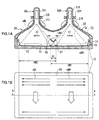
- a cathode ray tube As shown in FIGS. 1A and 1B, a cathode ray tube according to this embodiment comprises a panel portion 10 including a phosphor surface 11 inside, and a funnel portion 20 formed integrally with the panel portion 10. On the left and the right sides of the rear-end portion of the funnel portion 20, two long-and-narrow-shaped neck portions 30L and 30R each including built-in electron guns 31L and 31R are formed, respectively. As a whole, the cathode ray tube takes a double-funnel-shaped figure by the panel portion 10, the funnel portion 20, and the neck portions 30L and 30R.
- the outer portion forming the cathode ray tube is also called an outer vessel.
- Each opening of the panel portion 10 and the funnel portion 20 is fused to each other so that it is capable of keeping high-vacuum condition inside.
- a striped pattern (not shown) made of phosphors is formed. It is the phosphor surface 11 which mainly corresponds to one specific example of an "image display means" in the present invention.
- a color selection mechanism 12 made of a thin metal plate is positioned to face the phosphor surface 11.
- the color selection mechanism 12 is also called an aperture grill, a shadow mask or the like depending on the method being employed.
- the periphery of the color selection mechanism 12 is supported by a frame 13 and is installed on the inside surface of the panel portion 10 through a supporting spring 14.
- An anode portion (not shown) for applying anode voltage HV is provided in the funnel portion 20.
- Deflection yokes 21L and 21R for deflecting respective electron beams eBL and eBR irradiated from the electron guns 31L and 31R, respectively, and convergence yokes 32L and 32R for performing convergence of each electron beam for each color irradiated from respective electron guns 31L and 31R are installed in the peripheral portion extending from the funnel portion 20 to each of neck portions 30L and 30R.
- the inside surface extending from the neck 30 to the phosphor surface 11 of the panel portion 10 is covered with an inside conductive film 22.
- the inside conductive film 22 is electrically coupled to the anode portion (not shown) and is kept to the anode voltage HV.
- the peripheral surface of the funnel portion 20 is also covered with an external conductive film 23.
- Each electrode within the electron guns 31L and 31R performs control, acceleration and the like of the electron beams eBL and eBR emitted from the cathodes.
- Each of the electron beams for each color emitted from the electron guns 31L and 31R is irradiated onto the phosphors of the corresponding color on the phosphor surface 11 through the color selection mechanism 12 and the like, respectively.
- the left half of the screen and an area extending into the right half of the screen are drawn by the electron beam eBL from the electron gun 31L provided on the left side
- the right half of the screen and an area extending into the left half of the screen are drawn by the electron beam eBR from the electron gun 31R provided on the right side.
- the edges of the left and right divided screens are joined with the edges being overlapped each other.
- a single screen SA is formed to display an image. Accordingly, the center portion of the screen SA becomes an overlapped region OL where both right and left screens partially overlap.
- the phosphor surface 11 in the overlapped region OL is for both of the electron beams eBL and eBR.
- the line scan of the electron beam eBL from the left side electron gun 31L is performed in a horizontal deflection direction from right to left (X2 direction in FIG. 1A), and the field scan is performed in a vertical deflection direction from the top to the bottom.
- the line scan of the electron beam eBR from the right side electron gun 31R is performed in a horizontal deflection direction from left to right (X1 direction in FIG.1A), and the field scan is performed in a vertical deflection direction from the top to the bottom. Accordingly, in the example shown in FIG.
- the line scan of each of electron beams eBL and eBR is performed from the center to the right or left side of the screen in a horizontal direction, which is the opposite direction from each other, and the field scan is performed from the top to the bottom as in the common cathode ray tube.
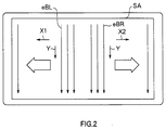
- the scanning of the electron beams eBL and eBR may be performed in a scanning direction different from those shown in FIG. 1B.
- the line scan by eBL and eBR is performed from the top to the bottom (Y direction shown in FIG. 2), and the field scans are performed from the center to the right or left side of the screen in a horizontal direction, which is the opposite direction from each other.
- the example shown in FIG.2 is the reversed of the one shown in FIG.1B wherein the line scan and the field scan by respective electron beams eBL and eBR.
- a V-shaped beam shield 27 as a shielding member against the electron beams eBL and eBR is provided in an overscanned region OS of the electron beams eBL and eBR on the joined side (the center of the whole screen in this embodiment) of the left and right divided screens adjacent to each other, so that the electron beams eBL and eBR, which have overscanned the overscanned region OS, do not unnecessarily reach the phosphor surface 11 and emit light.
- the beam shield 27 is provided by using the frame 13, as a base, for example, supporting the color selection mechanism 12.
- the beam shield 27 becomes the anode voltage HV by being electrically coupled to the inside conductive film 22 through the frame 13.
- the overscanned region is the outer region of each scanned region of the electron beams eBL and eBR forming the effective screen in each scanned region of the electron beams eBL and eBR.
- a region SW1 is an effective screen on the phosphor surface 11 of the electron beam eBR in a horizontal direction
- a region SW2 is an effective screen on the phosphor surface 11 of the electron beam eBL in a horizontal direction.
- FIG.3 shows a circuit example for inputting an analog composite signal in the NTSC (National Television System Committee) format as an inputted signal (video signal) D IN and, then, displaying a moving image based on the signal.
- the signal processing circuit shown in FIG. 3 corresponds to one specific example of the "brightness control apparatus" in the present invention.
- the cathode ray tube includes a composite/RGB converter 51 which converts an analog composite signal inputted one-dimensionally as a video signal D IN to signals for each of colors, R, G, B, for outputting, an analog/digital signal ("A/D" in the followings) converter 52 (52r, 52g, 52b) which converts analog signals for each of colors outputted from the composite/RGB converter 51, the frame memory 53 which stores digital signals for each color, outputted from the A/D converter 52, two-dimensionally in frame, and the memory controller 54 which generates a write address and a readout address of image data for the frame memory 53.
- An SDRAM synchronous dynamic random access memory
- the cathode ray tube includes a DSP (digital signal processor) circuit 50L, a DSP circuit 55L1, a frame memory 56L (56Lr, 56Lg, 56Lb), a DSP circuit 55L2 and a digital/analog signal ("D/A" in the followings) converter 57L (57Lr, 57Lg, 57Lb), which perform control on image data for the left side screen among image data for each color stored in the frame memory 53, and a DSP circuit 50R, a DSP circuit 55R1, a frame memory 56R (56Rr, 56Rg, 56Rb), a DSP circuit 55R2 and a D/A converter 57L (57Rr, 57Rg, 57Rb), which perform control on image data for the right side screen among image data for each color stored in the frame memory 53.
- DSP digital signal processor
- the DSP circuits 50L and 50R are circuits for brightness control, mainly provided for modulating and controlling brightness.
- other DSP circuits 55L1, 55L2, 55R1, 55R2 are circuits for positional control, mainly provided for correcting a position.
- the cathode ray tube includes a data for correction memory 60, a control portion 62A for brightness control, a control portion 62B and a memory controller 63.
- the data for correction memory 60 stores data for correction for each color for correcting a display condition of an image.
- the control portion 62A for brightness control is inputted image data for each color stored in the frame memory 53 and instructs a signal processing method, which should be done for brightness control for the DSP circuits 50L and 50R for brightness control, for example.
- the control portion 62B is inputted data for correction from the data for correction memory 60 and instructs an operation method, which should be done for position correction for the DSP circuit 55 for position correction, for example.
- the memory controller 63 generates a write address and a readout address of image data for the frame memories 56L and 56R.
- the control portion 62A has a memory, not shown, for storing a plurality of correction coefficients for each color corresponding to a plurality of signal levels used in brightness control.
- the control portion 62A mainly corresponds to one specific example of a "signal level detection means” and a “calculating means” in the present invention. Further, the DSP circuits 50L and 50R correspond to one specific example of a "brightness modulating means” in the present invention.
- the data for correction memory 60 has memory region for each color to store data for correction for each color in each memory region.
- the data for correction to be stored in the data for correction memory 60 is generated when a cathode ray tube is manufactured, for example.
- the data for correction is generated by measuring a distorted amount, a mis-convergence amount or the like of an image displayed in the cathode ray tube.
- a device for generating the data for correction is composed by an image pickup apparatus 64 to display an image in the cathode ray tube and a data for correction generating means to generate the data for correction on the basis of an image displayed the image pickup apparatus 64, not shown, for example.
- the image pickup apparatus 64 images an image displayed in the cathode ray tube.
- the image pickup apparatus 64 includes an imaging element such as a CCD (charge coupled device) and images a screen displayed on the surface of the cathode ray tube for each of colors R, G, B, to output the imaging screen as image data for each color.
- the data for correction generating means is composed by a microcomputer or the like and generates, as data for correction, data related to a moving amount of each pixel from a proper display position in discrete, two-dimensional image data, which represent the image imaged by the image pickup apparatus 64.
- the DSP circuits 50L and 50R for brightness control and the DSP circuit 55 (55L1, 55L2, 55R1, 55R2) for position correction are composed by one chip of a generic LSI (large-scale integrated circuit), for example.
- the DSP circuits 50L and 50R and the DSP circuits 55 follow instructions from the control portions 62A and 62B in order to correct the brightness in the overlapped region OL and to correct image distortion, mis-convergence, and the like that the cathode ray tube has and perform each kind of operation processing (signal processing) for inputted image data.
- the control portion 62B instructs an operation method for correcting a position mainly to each of DSP circuit 55 for position correction based on data for correction stored in the data for correction memory 60.
- the DSP circuit 50L performs signal processing related to brightness mainly on image data for the left side divided screen among image data for each color stored in the frame memory 53 and outputs for each color image data, on which the signal processing has been performed, to the DSP circuit 55L1. Further, the DSP circuit 55L1 performs correction processing of a position in the horizontal direction mainly on image data for each color outputted from the DSP circuit 50L and outputs the correction result for each color to the frame memory 56L. The DSP circuit 55L2 performs correction processing of a position mainly in the vertical direction on image data for each color stored in the frame memory 56L and outputs the correction result for each color to the D/A converter 57L.
- the DSP circuits 50R performs signal processing related mainly to brightness on image data for the right side divided screen among the image data for each color stored in the frame memory 53 and outputs the corrected image data for each color to the DSP circuit 55R1.
- the DSP circuit 55R1 performs correction processing of a position in the horizontal direction mainly on image data for each color outputted from the DSP circuit 50R and outputs the correction result for each color to the frame memory 56R.
- the DSP circuit 55R2 performs correction processing of a position in the vertical direction mainly on image data for each color stored in the frame memory 56R and outputs the correction result for each color to the D/A converter 57R.
- the DSP circuits 50L and 50R for brightness control and the control portion 62A can perform modulation control of brightness on a video signal depending on a horizontal pixel position and a signal level.
- the signal processing performed in the DSP circuits 50L and 50R and the control portion 62A is processing where a video signal is multiplied by a correction coefficient in order to change the degree of brightness, as described below.
- Each of the D/A converters 57L and 57R converts the operated image data outputted from each of DSP circuits 55L2, 55R2, respectively, to an analog signal and outputs the analog signal to the side of respective electron beams 31L and 31R.
- Each of the frame memories 56L and 56R stores the operated image data outputted from each of DSP circuits 55L1, 55R1, in frames, respectively, and outputs the stored image data for each color.
- the frame memories 56L and 56R are memories, which allow rapid random access, and an SRAM (static RAM) is used for them, for example. If the frame memories 56L and 56R are constructed by a single memory allowing rapid random access, a frame passing operation occurs while performing image data writing and reading operations, which causes image turbulence. Thus, two memories (double buffer) are used respectively, for the constructions of the frame memories 56L and 56R.
- the frame memories 56L and 56R perform the writing operation on the image data by following an order of a write address generated in the memory controller 63. Further, they perform the reading operation on the image data by following an order of a read-out address generated in the memory controller 63.
- the memory controller 63 can generate a write address of image data for frame memories 56L and 56R. It can also generate a read-out address of the image data stored in the frame memories 56L and 56R in an order different from the order of the write address. Since the orders of the read-out address and the write address can be generated separately in this embodiment, image data written in the frame memories 56L and 56R can be modified such that the image data can be read out with involving rotation and inversion of an image, for example. Thus, in this embodiment, the image conversion is performed on image data outputted from the DSP circuits 55L1 and 55R1 properly such that the image condition is suitable for the vertical correction operation done in the DSP circuits 55L2, 55R2.
- an analog composite signal inputted as a video signal D IN is converted to a video signal for each of colors, R, G, B by the composite/RGB converter 51 (FIG. 3.)
- the video signal is converted to a digital video signal for each color by the A/D converter 52. It is preferable to perform the IP (interlace progressive) conversion here because it makes subsequent processing easier.
- the digital video signal outputted from the A/D converter 52 is stored in the frame memory 53 for each color in frames by following a control signal Sa1, which indicates a write address generated in the memory controller 54.
- the image data in frame stored in the frame memory 53 are read out by following a control signal Sa2, which indicates a readout address generated in the memory controller 54 to output to the DSP circuits 50L and 50R for brightness control and the control portion 62A.
- image data for each color stored in the frame memory 53 signal processing mainly related to brightness is performed on image data for the left side divided screen through the function of the DSP circuit 50L based on a signal processing method instructed from the control portion 62A. Then, operation processing mainly for correcting an image positionally is performed on it through the function of the DSP circuit 55L1, the frame memories 56L and the DSP circuit 55L2 based on data for correction stored in data for correction memory 60.
- the image data for the left side divided screen on which the operation processing has been performed is converted to an analog signal through the D/A converter 57L to be supplied to a cathode, not shown, positioned inside of the left side electron gun 31L as cathode drive voltage.
- signal processing mainly related to brightness is performed on an image data for the right side divided screen through the function of the DSP circuit 50R based on a signal processing method instructed by the control portion 62A.
- operation processing mainly for correcting an image positionally is performed on it through the function of the DSP circuit 55R1, the frame memories 56R and the DSP circuit 55R2 based on data for correction stored in data for correction memory 60.
- the image data for the right side divided screen on which the operation processing has been performed is converted to an analog signal through the D/A converter 57R, and is supplied to a cathode which is not shown, positioned inside of the right side electron gun 31R as cathode driven voltage.
- Electron beams eBL and eBR is projected from electron guns 31L and 31R, according to the given cathode driving voltage, respectively.
- the cathode ray tube of this embodiment is capable of color display.
- the cathodes for each of colors, R, G, and B, are provided in each of electron guns 31L and 31R, and the electron beams for each color are projected from each of electron guns 31L and 31R.
- the electron beams eBL and eBR for each color projected from the electron guns 31L and 31R are converged by the magnetic function of the convergence yokes 32L and 32R, respectively.
- the electron beams scan the whole surface of the phosphor surface 11, deflected by the magnetic function of the deflection yokes 21L and 21R, and a desired image is displayed on the screen SA (FIGS. 1A and 1B) on the surface of the panel portion 10.
- the left half of the screen and the area extending into the right half of the screen are drawn by the electron beam eBL while the right half of the screen and the area extending into the left half of the screen are drawn by the electron beam eBR.
- a single screen SA is formed by partially joining the end portions of the left and the right divided screens formed in the manner described above.
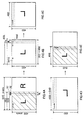
- FIG. 4A schematically shows an image data for the left side divided screen to be read out from the frame memory 53 and to be inputted to the DSP circuit 50L.
- An image data of 640 pixels wide by 480 pixels high for example, is written into the frame memory 53.
- the center region of 62 pixels wide (left side 32 pixels + right side 32 pixels) by 480 pixels high is an overlapped region OL of the left and the right divided screens.
- the left side image data of 352 pixels wide by 480 pixels high is read out, shown as a diagonally shaded area in FIG. 4A, and is inputted to the DSP circuit 50L.
- FIG. 4B schematically shows an image data to be written into the frame memories 56L after correction processing is processed on the image by the DSP circuit 50L and DSP circuit 55L1.
- the DSP circuit 50L performs the operation processing for correcting brightness in the overlapped region OL on an image data of 352 pixels wide by 480 pixels high shown as the shaded area in FIG. 4A independent of the positional correction before the DSP circuit 55L1 performs the correction processing.
- FIG. 4B shows an example of a modulation waveform 80L, which indicates correction of brightness in the left side divided screen, corresponding to the image data.
- the DSP circuit 55L1 performs the operation processing involving horizontal correction on an image data of 352 pixels wide by 480 pixels high, which is shown as the shaded area in FIG. 4A after the DSP circuit 50L performs the brightness correction processing.
- the operation processing enlarges the image horizontally to 352 pixels wide by 480 pixels high as shown in FIG. 4B, and generates an image data of 480 pixels wide by 480 pixels high.
- the DSP circuit 55L1 performs operation processing for correcting horizontal distortion and the like based on data for correction stored in the data for correction memory 60. Further, in order to extend the number of pixel, it is necessary to interpolate data related to a pixel, which does not exist in the original image.
- the image data, on which the operation processing is performed in the DSP circuit 50L and the DSP circuit 55L1, are stored for every color by following a control signal Sa3L, which indicates a write address generated in the memory controller 63.
- image data is written sequentially from upper left as a starting point to the right direction.
- the image data stored in the frame memory 56L are read out for each color following a control signal Sa4L, which indicates a readout address generated in the memory controller 63 and is inputted to the DSP circuit 55L2.
- the order of the write addresses and the order of the readout addresses for the frame memory 56L generated in the memory controller 63 are different.
- the readout address is arranged such that the image data is read out sequentially from the upper right as a starting point to the downward direction.
- FIG. 4C schematically shows an image data to be read out from the frame memory 56L and inputted to the DSP circuit 55L2.
- the image to be inputted to the DSP circuit 55L2 is converted to rotate counterclockwisely by 90° to the state of an image shown in FIG. 4B.
- the DSP circuit 55L2 performs the operation processing involving vertical correction on an image data (FIG. 4C) of 480 pixels wide by 480 pixels high, which has been read out from the frame memory 56L.
- the operation processing enlarges the image horizontally from 480 pixels to 640 pixels as shown in FIG. 4D, and generates image data of 640 pixels wide by 480 pixels.
- the DSP circuit 55L2 performs operation processing for correcting vertical distortion and the like based on data for correction stored in the data for correction memory 60 at the same time.
- the image as shown in the shaded area in FIG. 4E is displayed on the left side of the phosphor surface 11.
- the left side image displayed on the phosphor surface 11 is arranged to be properly displayed without distortion and the like.
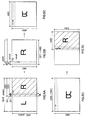
- FIG. 5A schematically shows an image data for the right side divided screen to be read out from the frame memory 53 and inputted to the DSP circuit 50R.
- the image data of 640 pixels wide by 480 pixels high for example, written into the frame memory 53
- the right side image data of 352 pixels wide by 480 pixels high are read out, shown as a diagonally shaded area in FIG. 5A, for example, and are inputted to the DSP circuit 50R.
- FIG. 5B shows an image data to be written into the frame memories 56R after correction processing is performed on the image by the DSP circuit 50R and DSP circuit 55R1.
- the DSP circuit 50R performs the operation processing for correcting brightness in the overlapped region OL on an image data of 352 pixels wide by 480 pixels high shown as the shaded area in FIG. 5A independent of the positional correction before the DSP circuit 55R1 performs the correction processing.
- FIG. 5B shows an example of a modulation waveform 80R, which indicates correction of brightness in the right side divided screen, corresponding to the image data.
- the DSP circuit 55R1 performs the operation processing involving horizontal correction on an image data of 352 pixels wide by 480 pixels high shown as the shaded area in FIG. 5A after the DSP circuit 50R performs the brightness correction processing.
- the operation processing enlarges the image horizontally to 352 pixels wide by 480 pixels as shown in FIG. 5B, and generates an image data of 480 pixels wide by 480 pixels high.
- the DSP circuit 55R1 operation processing is performed at the same time, for correcting horizontal distortion and the like based on data for correction stored in the data for correction memory 60.
- the image data, on which the operation processing has been performed in the DSP circuit 50R and the DSP circuit 55R1, are stored for every color by following a control signal Sa3R, which indicates a write address generated in the memory controller 63.
- a control signal Sa3R which indicates a write address generated in the memory controller 63.
- an image data is written sequentially from upper left as a starting point to the right direction.
- the image data stored in the frame memories 56R are read out for each color by following a control signal Sa4R, which indicates a readout address generated in the memory controller 63, and are inputted to the DSP circuit 55R2.
- the order of the write addresses and the order of the readout addresses for the frame memories 56R generated in the memory controller 63 are different.
- the readout address is arranged such that the image data are read out sequentially from the upper left as a starting point to the downward direction.
- FIG. 5C schematically shows an image data to be read out from the frame memories 56R and inputted to the DSP circuit 55R2.
- the image to be inputted to the DSP circuit 55R2 is converted to rotate counterclockwisely by 90° as well as to mirror-reverse to the state of an image shown in FIG.5B.
- the DSP circuit 55R2 performs the operation processing involving vertical correction on image data (FIG. 5C) of 480 pixels wide by 480 pixels high, read out from the frame memory 56R.
- the operation processing enlarges the image horizontally from 480 pixels to 640 pixels as shown in FIG. 5D, and generates an image data of 640 pixels wide by 480 pixels high.
- the DSP circuit 55R2 performs operation processing for correcting vertical distortion and the like based on data for correction stored in the data for correction memory 60 at the same time.
- the correction processing is performed on the inputted image data in view of distortion and the like, the right side image displayed on the phosphor surface 11 is arranged to be properly displayed without distortion and the like. Further, on the left and the right divided screens shown in FIG. 4E and FIG. 5E, brightness correction in the overlapped region OL are properly performed and correction relating to each of distortion and the like are properly performed, respectively. Thus, it allows proper image display with the joined part inconspicuous in brightness and position when the left and the right screens are joined.
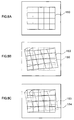
- Data for correction is indicated by a moving amount with regard to a reference point arranged in grid, for example.
- a pixel for each color located in a grid point (i,j) is as shown in FIG. 6B, respectively, by moving them for each of their moving amounts, where the rid point (i,j) shown in FIG.
- a moving amount in the X direction for the R color is Fr(i,j); a moving amount in the Y direction is Gr(i,j), a moving amount in the X direction for the G color is Fg(i,j); a moving amount in the Y direction is Gg(i,j), a moving amount in the X direction for the B color is Fb(i,j); and a moving amount in the Y direction is Gb(i,j).
- the image as shown in FIG. 6C can be obtained by combining each image shown in FIG. 6B.
- FIGS 7A and 8A show a left side or a right side divided screen on the frame memory 53.
- FIGS. 7B and 8B show an image to be outputted from the DSP circuit 55L2 or the DSP circuit 55R2 through the DSP circuit 55L1 or DSP circuit 55R1.
- FIGS. 7C and 8C show an image of a left side or a right side divided screen to be actually displayed on the phosphor surface 11.
- FIGS. 7A-7C show a modified condition of an inputted image where the correction operation by using data for correction has not been performed in the processing circuit shown in FIG. 3.
- an image 160 (FIG.7A) on the frame memory 53 and an image 161 (FIG. 7B) outputted from the DSP circuit 66L2 or the DSP circuit 55R2 have the same form as that of the inputted image.
- the image is distorted due to the characteristics owned by the cathode ray tube itself owns, and an image 162 modified as shown in FIG. 7C, for example, is displayed on the phosphor circuit 11.
- FIG. 7C the image shown in broken lines corresponds to an image, to be actually displayed.
- FIGS. 8A-8C show a variation of the inputted image, when the correction operation is performed in the processing circuit shown in FIG. 3.
- the correction operation is performed separately, for each of colors R, G, B.
- the correction operation uses different data for correction, for the operation for each color, while the operation method is the same for each color.
- the image 160 (FIG. 8A) on the frame memory 53 has the same form as that of the inputted image.
- the correction operation is performed by respective DSP circuits 55L1, 55L2, 55R1 and 55R2 where the image is modified based on data for correction in the direction opposed to that in the image modification performed on the inputted image in the cathode ray tube (the modification by the characteristic owned by the cathode ray tube owns, see FIG. 7C.)
- An image 163 after the operation was performed is shown in FIG. 8B.
- the image shown in broken lines is the image 160 on the frame memory 53 and corresponds to the image before the correction operation is performed.
- pixels 170 are arranged in grid on an integer position in X, Y coordinates.
- FIG. 9 shows an example of the operation in the case of only one pixel is noted and a condition where an R signal value (called "R value” in the followings), Hd, which is a pixel value of a pixel located at the coordinates (1,1) before the correction operation is performed by the DSP circuit 55, is moving to the coordinates (3,4) after the operation.
- R value an R signal value
- the scanning is performed based on the video signal, on which the correction operation processing has been performed by the DSP circuit 55 according to this embodiment, the scanning of the pixel on the coordinates (1,1) in the original video signal will be performed "before" the scanning of the pixel at the coordinates (3,4) in the original video signal.
- the two-dimensional arrangement condition of pixels is re-arranged based on the data for correction and the like, and, as a result, the correction processing is performed such that an original one-dimensional video signal is varied in pixel timelikely and spacelikely.
- FIGS. 10A and 10B it will be explained for the case when a video signal of 720 pixels wide by 480 pixels high, for example, is inputted, and the left and the right divided screens SL, SR are formed such that the areas of 48 pixels wide by 480 pixels high as a center portion of the screen, which are indicated by the input video signal, are overlapped. That is, another description is also shown for the case when video signals for 384 pixels wide by 480 pixels high are inputted to DSP circuits 50L and 50R, respectively, as shown in FIGS. 10A and 10B.
- the code O1 indicates a centerline in the whole screen area.
- the DSP circuits 50L and 50R and the control portion 62A are capable of performing signal processing on the inputted video signals for controlling the degree of brightness depending on a pixel position in the horizontal direction (the overlapped direction).
- the DSP circuits 50L and 50R and the control portion 62A gradually increase the level of brightness from the starting point P1L, P1R of the overlapped region OL, and vary the level of the brightness in a curve to form a brightness gradient for example, so that the level of the brightness reaches maximum at the end points P2L and P2R in the overlapped region OL, and beyond that part, performs the modulation control on the degree of brightness to keep the level of the brightness constant to the end of the screen, in the region other than the overlapped region OL.
- FIG. 10C shows the level of brightness by matching it with the pixel position in each of divided screens shown in FIG. 10B. Also, in FIG. 10C, as an example, the maximum value of the brightness level is 1 and the minimum value of the brightness level is 0.
- the brightness gradient in the overlapped region OL may be formed in a sine or cosine function or a quadratic curve. Optimizing the form of the brightness gradient allows the brightness changes in the overlapped region OL to be appeared naturally, and also allows a larger margin for a positional error in overlapping the left and the right divided screens SL and SR.
- the DSP circuits 50L and 50R and the control portion 62A may perform modulation control of brightness based on a signal level in addition to the modulation control of brightness based on the pixel position in the joined direction described above. Next, the modulation control of brightness based on a signal level will be explained.
- one factor for determining the degree of brightness is a gamma value.
- the gamma value is different depending on the signal level of an inputted video signal, as described with reference to FIG. 24.
- a video signal is inputted from the frame memory 53 to the control portion 62A and the DSP circuits 50L and 50R.
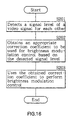
- the control portion 62A detects the level of a video signal for each color for each unit pixel or unit pixel array (Step S101) during the step where video signals are divided for the left and the right divided screens, that is, video signals for the left and the right divided screens are inputted from the frame memory 53 to the DSP circuits 50L and 50R, for example.
- the control portion 62A calculates an appropriate correction coefficient for each color, which should be used in the modulation control of brightness, among a plurality of correction coefficients stored in its own memory in advance based on the detected signal level (Step S102).
- the control portion 62A instructs the DSP circuits 50L and 50R to modulate brightness by using the determined correction coefficient.
- the DSP circuits 50L and 50R perform the modulation control of brightness on video signals following the instruction by the control portion 62A (Step S103).
- the DSP circuits 50L and 50R perform the signal processing where the video signals are multiplied by the correction coefficients, for example.
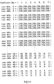
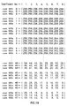
- FIG. 11 shows specific examples of correction coefficients for the left side divided screen
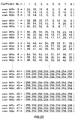
- FIG. 12 shows specific examples of correction coefficients for the right side divided screens.
- the degree of brightness is controlled such that the brightness gradient is formed in a sine or cosine function in the horizontal direction in the overlapped region OL.
- the brightness gradient is achieved by multiplying the video signals by correction coefficients k1 and k2 depending on each of pixel positions in the left and the right divided screen, as shown in the equations (2) and (3) described above, in practice.
- a different correction coefficient is used depending on the signal level of the video signal.
- correction coefficients shown in FIGS. 11 and 12 are actually stored in a memory within the control portion 62A as a table form program.
- the tables related to correction coefficients shown in FIGS.11 and 12 may be stored in a memory, which is provided in the outside of the control portion 62A separately for storing a table of correction coefficients.
- the cram WRx0 is a correction coefficient group, which is applied to a video signal for an R color at a 0th (or first) row of pixel positions in the horizontal direction in the overlapped region OL, for example.
- the Cram WGx0 is a correction coefficient group, which is applied to a video signal for a G color at a 0th row of pixel positions in the horizontal direction in the overlapped region OL, for example.
- the Cram WBx0 is a correction coefficient group, which is applied to a video signal for a B color at a 0th row of pixel positions in the horizontal direction in the overlapped region OL, for example.
- the point P2L (P1R) shown in FIG. 10 would be a 0th row of pixel positions in the horizontal direction and a position of the point P1L (P2R) would be a 47th (or 48th) row of pixel positions, here, for example.
- the correction coefficient group is prepared enough for pixel rows in the direction of joining screens in the overlapped region OL.
- the overlapped region OL consists of 48 pixels in the horizontal direction (the direction of joining).
- correction coefficients enough for 48 rows are prepared (cram WRx0 - cram WRx47 for the R color, for example).
- a group of seven correction coefficients corresponding to a signal level is prepared for each color for each pixel row.
- seven values for each color and for each pixel row within " ⁇ ⁇ " indicate correction coefficient values, respectively, and have respective coefficient numbers, first, second....in order from the left.
- a coefficient to be actually multiplied by a video signal actually is a value produced by reducing a value shown in FIGS. 11 and 12 by 1/256. That is, in FIGS. 11 and 12, a value of a correction coefficient, 256 is 1 actually.
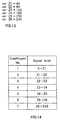
- FIGS. 13 and 14 a correspondence relationship between a correction coefficient and a signal level of a video signal shown in FIGS. 11 and 12 will be explained.
- Each value shown in FIGS. 13 and 14 is stored in a program form in a memory within the control portion 62.
- a memory may be provided separately in the outside of the control portion 62A to store a value.
- signal levels are divided to 256 division by matching with 256 levels of brightness and classified to seven signal level regions. More specifically, signal levels are classified to seven signal level regions at values 40(var ZI), 80 (var Z2), 120 (var Z3), 160 (var Z4), 200 (var Z5), and 240 (var Z6).
- a correspondence relationship between correction coefficients and each signal level region shown in FIG. 13 is as shown in FIG. 14, for example.
- the 0-Z1 signal level region is matched with the first correction number in the correction coefficient group shown in FIGS. 11 and 12. Also, in the example shown in FIG.
- signal levels of Z1-Z2, Z2-Z3, Z3-Z4, Z4-Z5, Z5-Z6, and Z6-255 are matched with 2nd, 3rd, 4th, 5th, 6th, and 7th coefficient numbers, respectively.
- the control portion 62A determines whether a signal level of a video signal is any of signal level regions and selects a correction coefficient corresponding to the determined signal level region.
- DSP circuits 50L and 50R perform signal processing in order to modulate brightness on a video signal by using the selected correction coefficient.
- correction coefficients shown in FIGS. 11-14 are only one example, the values and the like used in brightness control are not limited to those shown in FIGS.11-14.
- FIGS 11 and 12 while seven correction coefficients are prepared for each color and for each pixel row, correction coefficients more or less than seven may be used.
- a plurality of correction coefficients for each color associated depending on a plurality of signal levels are stored in advance, and among a plurality of correction coefficient, an appropriate correction coefficient to be used for brightness modulation control, is obtained for each color.
- brightness modulation control depending on a signal level is performed on each of a plurality of video signals such that a total sum of brightness at the same pixel position in the overlapped region on a screen, which is scanned based on the plurality of video signals equal to brightness at the same pixel position on an original image. Therefore, brightness control of the left and the right divided screen can be performed properly depending on a signal level of a video signal so that the joined part appears inconspicuous.
- the brightness modulation control is performed depending on a signal level allowing improvement in brightness inconsistencies in all the shades of gray. Therefore, even when a signal level always varies as of a moving picture, proper brightness control can be performed such that the joined part appears inconspicuous. Further, since the brightness modulation control is performed for each color, it is possible to improve brightness inconsistencies due to a difference in gamma characteristic for each color. Further, since it is possible to change a correction coefficient for each of the left and the right divided screens, it is possible to perform brightness modulation control depending on a characteristic of the left and the right electron guns 31L and 31R. By using those technologies described above, in a cathode ray tube with multiple electron guns, an image quality equal to or better than that with a general single electron gun can be achieved.
- brightness modulation control is performed depending on a pixel position in a direction orthogonal to a direction of joining a plurality of divided screens, instead of brightness modulation control depending on a signal level as in the first embodiment described above.
- brightness modulation control as a feature part in this embodiment, will be described in detail which is performed in the DSP circuits 50L and 50R and the control portion 62A.
- DSP circuits 50L and 50R perform signal processing for controlling a degree of brightness depending on a pixel position in the horizontal direction and the vertical direction with respect to inputted video signals.
- the control portion 62A has a memory, not shown, for storing a plurality of correction coefficients for each color corresponding to a pixel position used in brightness control.
- a video signal is inputted from the frame memory 53 to the control portion 62A and the DSP circuits 50L and 50R.
- the control portion 62A detects a pixel position in horizontal and vertical directions of video signals for each color (Step S201) during the step, for example, where video signals are divided for the left and the right divided screens, that is, video signals for the left and the right divided screens are inputted from the frame memory 53 to the DSP circuits 50L and 50R.
- the control portion 62 A obtains an appropriate correction coefficient for each color to be used in the modulation control of brightness, for every unit pixel among a plurality of correction coefficients stored in its own memory in advance based on the detected pixel position (Step S202).
- the control portion 62A instructs the DSP circuits 50L and 50R to modulate brightness by using the determined correction coefficient.
- the DSP circuits 50L and 50R perform the modulation control of brightness on video signals following the instruction by the control portion 62A (Step S203).
- the DSP circuits 50L and 50 R perform the signal processing wherein a video signal is multiplied by correction coefficients, as the modulation control of brightness.
- FIG. 19 shows specific examples of correction coefficients for the left side divided screen
- FIG. 20 shows specific examples of correction coefficients for the right side divided screens.
- a degree of brightness is controlled such that a brightness gradient is formed in a sine or cosine function in the horizontal direction in the overlapped region OL.
- a different correction coefficient is used depending on a pixel position in the vertical direction.
- correction coefficients shown in FIGS. 19 and 20 are actually stored in a memory within the control portion 62A as a table form program.
- the tables related to correction coefficients shown in FIGS. 19 and 20 may be stored in a memory, which is provided in the outside of the control portion 62A separately for storing a table of correction coefficients.
- the cram WRx0 is a correction coefficient group applied to a video signal for an R color at a 0th (or first) row of pixel positions in the horizontal direction in the overlapped region OL, for example.
- the cram WGx0 is a correction coefficient group applied to a video signal for a G color at a 0th row of pixel positions in the horizontal direction in the overlapped region OL, for example.
- the cram WBx0 is a correction coefficient group applied to a video signal for a B color at a 0th row of pixel positions in the horizontal direction in the overlapped region OL, for example.
- the point P2L (P1R) shown in FIG. 10 would be a 0th row of pixel positions in the horizontal direction and a position of the point P1L (P2R) would be a 47th (or 48th) row of pixel positions, for example.
- the correction coefficient group is prepared enough for pixel rows in the direction of overlapping screens in the overlapped region OL.
- the overlapped region OL consists of 48 pixels in the horizontal direction (the direction of overlapping).
- correction coefficients enough for 48 rows are prepared (cram WRx0 - cram WRx47 for the R color, for example).
- FIGS. 19 and 20 eight correction coefficients corresponding to a pixel position in the horizontal direction is prepared for each pixel row.
- eight values for each color and for each pixel row within " ⁇ ⁇ " indicate correction coefficient values, respectively, and have respective coefficient numbers, first, second....in order from the left.
- a coefficient to be actually multiplied by a video signal is a value produced by reducing a value shown in FIGS. 19 and 20 by 1/256. That is, in FIGS. 19 and 20, a value of a correction coefficient, 256, for example, is actually 1.
- a table shown in FIG. 21 is stored in a memory within control portion 62, by the same manner in which a correction coefficient is stored.
- a memory may be provided separately in the outside of the control portion 62A to store a numerical value.
- 480 pixels in the vertical direction are equally divided into eight regions including regions Y1-Y8 from the top of the screen.
- Eight coefficient numbers shown in FIGS. 19 and 20 are associated with region Y1-Y8 equally divided in this manner. That is, 1st, 2nd, 3rd, 4th, 5th, 6th, 7th and 8th coefficient numbers are associated with 1-60(Y1)th, 61-120(Y2)th, 121-180(Y3)th, 181-240(Y4)th, 241-300(Y5)th, 301-360(Y6)th, 361-420(Y7)th and 421-480(Y8)th pixels, respectively, as shown in FIG. 21, for example. Following the correspondence relationship shown in FIG.
- control portion 62A selects a correction coefficient corresponding to a pixel position in the vertical direction.
- DSP circuits 50L and 50R perform signal processing in order to modulate brightness on a video signal, using the correction coefficient selected in this manner.
- brightness modulation control is performed which corresponds to a pixel position in the horizontal and vertical directions.
- correction coefficients shown in FIGS. 19-21 are only one example, and a numerical value used in brightness control is not limited to those.
- a numerical value used in brightness control is not limited to those.
- FIGS 19 and 21 while eight correction coefficients are prepared for each color and for each pixel row, correction coefficients more or less than eight may be used.
- a plurality of correction coefficients for each color associated depending on a pixel position in the horizontal and the vertical directions are stored in advance, and an appropriate correction coefficient to be used for brightness modulation control is obtained for each color based on a pixel position in the horizontal and vertical directions.
- brightness modulation control depending on a pixel position is performed on each of a plurality of video signals such that a sum of brightness at the same pixel position in the overlapped region on a screen which is scanned based on the plurality of video signals, equals to brightness at the same pixel position on an original image. Therefore, brightness control of the left and the right divided screens can be performed properly on all over the overlapped region OL so that the joined part appears inconspicuous.
- a spot characteristic of an electron beam differs depending on a pixel position, and especially, there is a significant difference between that in a screen center portion and in a screen end portion.
- it is possible to perform brightness modulation in a vertical direction brightness inconsistencies due to the spot characteristic can be improved even if there is a significant difference in the spot characteristic between a center potion and a top and a bottom end portions in the overlapped region OL.
- a variation is caused in a light-emitting characteristic of a phosphors depending on a position of the phosphor surface 11.
- the brightness modulation control is performed depending on a pixel position, the brightness inconsistencies due to a light-emitting characteristic can be improved by determining a correction coefficient in view of a light-emitting characteristic of the phosphors.
- a varied light-emitting characteristic of the phosphors can be obtained by measuring a light-emitting amount of the phosphors when a cathode ray tube is manufactured, for example.
- the brightness modulation control in the first embodiment and the brightness modulation control in the second embodiment may be combined so that brightness modulation control may be performed depending on a signal level, a pixel position in an overlapped direction, and a pixel position in a direction orthogonal to the overlapped direction.
- a correction coefficient is changed properly depending on a signal level or a pixel position.
- a correction coefficient may be changed depending on another factor.
- the characteristic of the electron gun is a gamma characteristic of the electron gun or a current characteristic or the like of the electron gun.
- the current characteristic of the electron gun includes a characteristic related to a drive voltage supplied to the electron gun and a value of current flowing inside of the electron gun.
- a difference in the characteristic of the electron gun causes a difference in an electron amount emitted for a drive voltage supplied to the electron gun, it affects a degree of brightness.
- FIG. 1B shows an example where line scanning by each of electron beams eBL and eBR is performed from the center to the end of a screen, in the opposite direction to each other and field scanning is performed from the top to the bottom as in a general cathode ray tube.
- the scanning direction of each of electron beams eBL and eBR is not limited to this, and it is possible to perform line scanning from the end to the center of the screen, for example.
- the field scanning by each of electron beams eBL and eBR is performed from the center to the end of a screen, in the opposite direction to each other.
- the field scanning may be aligned in the same direction.
- the example is described where an analog composite signal in the NTSC system is used as a video signal D IN .
- the video signal D IN is not limited to that.
- an RGB analog signal can be used as the video signal D IN .
- the RGB signal may be obtained without the composite/RGB converter 51 (FIG.3).
- a digital signal used in a digital television may be inputted as the video signal D IN .
- the digital signal may be obtained directly without passing through the A/D converter 52 (FIG.3).
- a circuit from the frame memory 53 may have the same circuit configuration in the circuit example shown in FIG. 3.
- the frame memories 56L and 56R may be omitted from the configuration so that image data outputted from the DSP circuits 55L1 and 55R1 are directly supplied to the electron guns 31L and 31R through the DSP circuits 55L2 and 55R2.
- the correction in the vertical direction is performed after the correction in the horizontal direction is performed on an inputted image data.
- the correction in the horizontal direction may be conversely performed after the correction in the vertical direction is performed.
- correction of inputted image data is performed at the same time as enlargement of an image.
- the correction of image data may be performed without involving the enlargement of an image.
- the present invention is not limited to a cathode ray tube and applicable to various image display devices, such as a projection type image display device, where an image displayed in a cathode ray tube or the like through a projection optical system is enlarged and projected on a screen.
- the correction processing with regard to brightness and the positional correction processing are performed separately.
- the DSP circuits 50L and 50R for brightness control may be omitted from configuration elements and processing with regard to brightness in DSP circuits 50L and 50R may be performed at the same time as the operation processing for enlarging an image and correcting an image distortion and the like.
- the correction processing with regard to brightness is performed before the positional correction processing.
- DSP circuits 50L and 50R for brightness control may be located in the rear stage of the DSP circuits 55L2 and 44R2 so that the correction processing with regard to brightness can be performed after the positional correction processing.
- the processing for correcting the image distortion may be performed by optimizing a deflection magnetic field, which causes a deflection yoke.
- controlling image data directly by using data for correction can reduce image distortion and mis-convergence. Therefore, it is more preferable than a method where an image is adjusted by deflection yoke or the like. In order to eliminate image distortion by deflection yoke or the like, for example, it is necessary to distort the deflection magnetic field.
- the deflection magnetic field can be a uniform magnetic field, which enhances a focus characteristic.
Landscapes
- Engineering & Computer Science (AREA)
- Theoretical Computer Science (AREA)
- Remote Sensing (AREA)
- Physics & Mathematics (AREA)
- Computer Hardware Design (AREA)
- General Physics & Mathematics (AREA)
- Radar, Positioning & Navigation (AREA)
- Manufacturing & Machinery (AREA)
- Transforming Electric Information Into Light Information (AREA)
- Controls And Circuits For Display Device (AREA)
- Picture Signal Circuits (AREA)
- Video Image Reproduction Devices For Color Tv Systems (AREA)
- Details Of Television Scanning (AREA)
- Processing Of Color Television Signals (AREA)
Abstract
Description
Claims (13)
- A cathode ray tube for performing color image display by forming a single screen by joining a plurality of divided screens being formed by scanning of the plurality of electron beams by partially overlapping each other, comprising:a signal dividing means for dividing an inputted video signal into a video signal for the plurality of divided screens;a storage means for storing a plurality of correction coefficient for each color corresponding to a plurality of signal levels;a signal level detection means for detecting a signal level of an input video signal for each color;a calculating means for calculating an appropriate correction coefficient for each color to be used for modulation control of brightness among a plurality of correction coefficient stored in the storage means on the basis of the signal level detected by the signal level detection means.;a brightness modulation means for performing control corresponding to a signal level on each of the plurality of video signals for a divided screen so that the sum total of brightness at the same pixel position in an overlapped region on the screen, scanned on the basis of the plurality of video signals for the divided screens, equals to brightness at the same pixel position on an original image by using a correction coefficient for each color calculated through the calculating means; anda plurality of electron guns for emitting a plurality of electron beams, which scans said plurality of divided screens based on a video signal where modulation control has been performed by said brightness modulation means.
- A cathode ray tube according to claim 1, wherein:the plurality of correction coefficient stored in the storage means are associated depending on a pixel position in an overlapped direction of a plurality of divided screens in addition to a signal level;the calculating means calculates an appropriate correction coefficient, to be used for modulation control of brightness, for each color among the plurality of correction coefficients stored in the storage means based on a pixel position in the overlapped direction and a signal level detected by the signal level detecting means; andthe brightness modulation means performs modulation control of brightness corresponding to a pixel position in the overlapped direction on each of the plurality of video signals for divided screens by using the correction coefficient calculated by the calculating means.
- A cathode ray tube according to claim 1, wherein:the plurality of correction coefficient stored in the storage means are associated depending on a pixel position in an overlapped direction of a plurality of divided screens and a pixel position in a direction orthogonal to the overlapped direction in addition to the signal level;the calculating means calculates an appropriate correction coefficient to be used for modulation control of brightness, for each color among the plurality of correction coefficients stored in the storage means based on a pixel position in the overlapped direction, a pixel position in a direction orthogonal to the overlapped direction and a signal level detected by the signal level detecting means; andthe brightness modulation means performs modulation control of brightness corresponding to a pixel position in the overlapped direction and a pixel position in a direction orthogonal to the overlapped direction on each of the plurality of video signals for divided screens by using the correction coefficient calculated by the calculating means.
- A cathode ray tube according to claim 1, wherein:the plurality of correction coefficient stored in the storage means are associated depending on a characteristic of the plurality of electron guns in addition to a signal level;the calculating means calculates an appropriate correction coefficient to be used for modulation control of brightness, for each color among a plurality of correction coefficients stored in the storage means based on a characteristic of the plurality of electron guns and a signal level detected by the signal level detecting means; andthe brightness modulation means performs modulation control of brightness corresponding to a characteristic of the plurality of electron guns on each of the plurality of video signals for divided screens by using the correction coefficient calculated by the calculating means.
- A cathode ray tube according to claim 1, further comprising:the positional control means controls an inputted one-dimensional video signal to be converted into a dispersed two-dimensional image data, and varies and corrects a pixel array condition of the two-dimensional image data timelikely and spacelikely, for each of the divided screens and for each color, so that the plurality of divided screens are joined and displayed in an appropriate position, when the image is displayed, after that, the positional control means controls the corrected image, data to be converted to one-dimensional video signals again and to be outputted.
- An apparatus for controlling brightness for performing brightness control of an image displayed in an image display device, which forms a single screen by joining a plurality of divided screens by partially overlapping each other, wherein the apparatus for controlling brightness comprises:a signal level detection means for detecting a signal level of an inputted video signal for divided screen;a storage means for storing a plurality of correction coefficient corresponding to a plurality of signal levels;a calculating means for calculating an appropriate correction coefficient to be used for modulation control of brightness among a plurality of correction coefficient stored in the correction coefficient storage means; anda brightness modulation means for performing control corresponding to a signal level on each of the plurality of video signals for a divided screen so that the sum total of brightness at the same pixel position in an overlapped region on the screen, which is scanned on the basis of the plurality of video signals for the divided screen, equals to brightness at the same pixel position on an original image by using a correction coefficient for each color calculated through the calculating means.
- An apparatus for controlling brightness according to claim 6 wherein control of brightness depending on a signal level is performed for each color.
- An apparatus for controlling brightness according to claim 6, wherein:a plurality of correction coefficients stored in the storage means are associated depending on a pixel position in an overlapped direction of a plurality of divided screens in addition to a signal level;the calculating means calculates an appropriate correction coefficient to be used for modulation control of brightness, for each color among a plurality of correction coefficients stored in the storage means based on a pixel position in the overlapped direction and a signal level detected by the signal level detecting means; andthe brightness modulation means performs modulation control of brightness corresponding to a pixel position in the overlapped direction on each of the plurality of video signals for divided screens by using the correction coefficient calculated by said calculating means.
- An apparatus for controlling brightness according to claim 6, wherein:the plurality of correction coefficients stored in the storage means are associated depending on a pixel position in an overlapped direction of a plurality of divided screens and a pixel position in a direction orthogonal to the overlapped direction in addition to the signal level;the calculating means calculates an appropriate correction coefficient to be used for modulation control of brightness, for each color among the plurality of correction coefficients stored in the storage means based on a pixel position in the overlapped direction, a pixel position in a direction orthogonal to the overlapped direction and a signal level detected by the signal level detecting means; andthe brightness modulation means performs modulation control of brightness corresponding to a pixel position in the overlapped direction and a pixel position in a direction orthogonal to the overlapped direction on each of the plurality of video signals for divided screens by using the correction coefficient calculated by the calculating means.
- An apparatus for controlling brightness according to claim 6, wherein:the image display device comprises a plurality of electron guns for emitting a plurality of electron beams and is a cathode ray tube, which performs image display by emitting the plurality of electron beams for scanning the plurality of divided screens from the plurality of electron guns based on a video signal after modulation control was performed by the brightness modulation means
- An apparatus for controlling brightness according to claim 10, wherein:the plurality of correction coefficients stored in the storage means are associated depending on a characteristic of the plurality of electron guns in addition to a signal level;the calculating means calculates an appropriate correction coefficient to be used for modulation control of brightness, for each color among a plurality of correction coefficients stored in the storage means based on a characteristic of the plurality of electron guns and a signal level detected by the signal level detecting means; andthe brightness modulation means performs modulation control of brightness corresponding to a characteristic of the plurality of electron guns on each of the plurality of video signals for divided screens by using the correction coefficient obtained by the calculating means.
- An apparatus for controlling brightness according to claim 6, further comprising:the positional control means for performing control where an inputted one-dimensional video signal is converted to a dispersed two-dimensional image data and for performing control where a pixel array condition in the two-dimensional image data is corrected by being varied timelikely and spacelikely for each divided screen and the corrected image data is converted to a one-dimensional video signal again for outputting so that the plurality of divided screens are joined and displayed properly in position when image display is performed.
- A method for controlling brightness for performing brightness control of an image displayed in an image display device, which forms a single screen by joining a plurality of divided screens by partially overlapping each other, wherein the method for controlling brightness comprises steps of:detecting a signal level of an inputted video signal;storing a plurality of correction coefficients corresponding to a plurality of signal levels in a storage means;calculating an appropriate correction coefficient to be used for modulation control of brightness, among a plurality of correction coefficients stored in the storage means; andperforming modulation control of brightness corresponding to a signal level on each of the plurality of video signals for a divided screen so that the sum total of brightness at the same pixel position in an overlapped region on the screen, which is scanned based on the plurality of video signals for the divided screens, equals to brightness at the same pixel position on an original image by using the calculated.
Applications Claiming Priority (4)
| Application Number | Priority Date | Filing Date | Title |
|---|---|---|---|
| JP15966899 | 1999-06-07 | ||
| JP15966899 | 1999-06-07 | ||
| JP2000091170 | 2000-03-29 | ||
| JP2000091170A JP2001056658A (en) | 1999-06-07 | 2000-03-29 | Cathode ray tube and brightness control device and method |
Publications (2)
| Publication Number | Publication Date |
|---|---|
| EP1059625A2 true EP1059625A2 (en) | 2000-12-13 |
| EP1059625A3 EP1059625A3 (en) | 2002-05-29 |
Family
ID=26486390
Family Applications (1)
| Application Number | Title | Priority Date | Filing Date |
|---|---|---|---|
| EP00304762A Withdrawn EP1059625A3 (en) | 1999-06-07 | 2000-06-06 | Cathode ray tube and apparatus and method of controlling brightness |
Country Status (6)
| Country | Link |
|---|---|
| US (1) | US6545718B1 (en) |
| EP (1) | EP1059625A3 (en) |
| JP (1) | JP2001056658A (en) |
| KR (1) | KR20010014996A (en) |
| CN (1) | CN1201369C (en) |
| TW (1) | TW459264B (en) |
Families Citing this family (4)
| Publication number | Priority date | Publication date | Assignee | Title |
|---|---|---|---|---|
| US20030016302A1 (en) * | 2001-07-09 | 2003-01-23 | Brian Fudge | Apparatus and method for conditioning digital image data for display of the image represented thereby |
| EP1578584A4 (en) * | 2002-11-12 | 2008-07-30 | Entegris Inc | Process and apparatus for molding polymer fittings |
| JP2009042348A (en) * | 2007-08-07 | 2009-02-26 | Panasonic Corp | Plasma display apparatus and driving method of plasma display panel |
| JP2010139782A (en) | 2008-12-11 | 2010-06-24 | Sony Corp | Display device, method for driving the display device, and program |
Family Cites Families (11)
| Publication number | Priority date | Publication date | Assignee | Title |
|---|---|---|---|---|
| JPS5017167A (en) | 1973-06-11 | 1975-02-22 | ||
| US4792720A (en) | 1985-12-09 | 1988-12-20 | Kabushiki Kaisha Toshiba | Color cathode ray tube |
| US5136390A (en) | 1990-11-05 | 1992-08-04 | Metavision Corporation | Adjustable multiple image display smoothing method and apparatus |
| JP3566314B2 (en) | 1992-04-13 | 2004-09-15 | メタビジョン コーポレイション | Adjustable composite image display smoothing method and apparatus |
| DE4240353A1 (en) | 1992-12-01 | 1994-06-09 | Thomson Brandt Gmbh | Picture tube with a variety of cannons |
| MY114546A (en) | 1995-02-03 | 2002-11-30 | Toshiba Kk | Color cathode-ray tube |
| JP3488313B2 (en) * | 1995-04-21 | 2004-01-19 | ソニー株式会社 | Video signal processing device and composite screen projection device |
| EP0968515A1 (en) | 1997-12-23 | 2000-01-05 | Koninklijke Philips Electronics N.V. | Crt with at least two yokes and electron guns |
| US6340976B1 (en) * | 1998-04-15 | 2002-01-22 | Mitsubishi Denki Kabushiki Kaisha | Multivision system, color calibration method and display |
| US6456339B1 (en) * | 1998-07-31 | 2002-09-24 | Massachusetts Institute Of Technology | Super-resolution display |
| TW451247B (en) * | 1999-05-25 | 2001-08-21 | Sony Corp | Image control device and method, and image display device |
-
2000
- 2000-03-29 JP JP2000091170A patent/JP2001056658A/en active Pending
- 2000-05-31 TW TW089110628A patent/TW459264B/en not_active IP Right Cessation
- 2000-06-05 KR KR1020000030780A patent/KR20010014996A/en not_active Withdrawn
- 2000-06-05 US US09/587,471 patent/US6545718B1/en not_active Expired - Fee Related
- 2000-06-06 EP EP00304762A patent/EP1059625A3/en not_active Withdrawn
- 2000-06-07 CN CNB001264354A patent/CN1201369C/en not_active Expired - Fee Related
Also Published As
| Publication number | Publication date |
|---|---|
| TW459264B (en) | 2001-10-11 |
| KR20010014996A (en) | 2001-02-26 |
| CN1281243A (en) | 2001-01-24 |
| CN1201369C (en) | 2005-05-11 |
| JP2001056658A (en) | 2001-02-27 |
| US6545718B1 (en) | 2003-04-08 |
| EP1059625A3 (en) | 2002-05-29 |
Similar Documents
| Publication | Publication Date | Title |
|---|---|---|
| TW448685B (en) | Image display correcting system, image display correcting apparatus and method, and image display apparatus and method | |
| JP2693419B2 (en) | Color image receiving device | |
| US6466268B1 (en) | Image control device and method, and image display device | |
| US6545718B1 (en) | Cathode ray tube and apparatus and method of controlling brightness | |
| US6580233B2 (en) | Cathode ray tube and intensity controlling method | |
| JP3068115B1 (en) | Cathode ray tube and image correction method | |
| US6452636B1 (en) | Image control device and method, and image display device | |
| JP3178526B2 (en) | Image correction apparatus and method, and image display apparatus | |
| JP3057230B1 (en) | Image correction apparatus and method, and image display apparatus | |
| JP3187787B2 (en) | Image control apparatus and method, and image display apparatus | |
| EP1174848A2 (en) | Cathode ray tube and image control device | |
| JP2001042848A (en) | Image control apparatus and method, and image display apparatus | |
| JP2558462B2 (en) | Driving method of flat cathode ray tube | |
| JP3417394B2 (en) | Cathode ray tube and signal detection method in cathode ray tube | |
| JP2002351376A (en) | Cathode ray tube, scanning control device therefor, and scanning method therefor | |
| AU2001100380A4 (en) | Entirely-D.S.P.-based correction for design-based distortion and outer pin-cushion mis-alignment in direct-view C.R.T's. | |
| JP2002245955A (en) | Electron beam position detection mechanism and cathode ray tube | |
| JP2002341816A (en) | Cathode ray tube, its driving device, and its driving method | |
| JPH0666930B2 (en) | Driving method of flat cathode ray tube | |
| JPH0537945A (en) | Index tube | |
| JPH11146412A (en) | Digital image correction device | |
| JP2001083922A (en) | Double electron gun type image display | |
| JPH08221026A (en) | Display device |
Legal Events
| Date | Code | Title | Description |
|---|---|---|---|
| PUAI | Public reference made under article 153(3) epc to a published international application that has entered the european phase |
Free format text: ORIGINAL CODE: 0009012 |
|
| AK | Designated contracting states |
Kind code of ref document: A2 Designated state(s): AT BE CH CY DE DK ES FI FR GB GR IE IT LI LU MC NL PT SE |
|
| AX | Request for extension of the european patent |
Free format text: AL;LT;LV;MK;RO;SI |
|
| PUAL | Search report despatched |
Free format text: ORIGINAL CODE: 0009013 |
|
| AK | Designated contracting states |
Kind code of ref document: A3 Designated state(s): AT BE CH CY DE DK ES FI FR GB GR IE IT LI LU MC NL PT SE |
|
| AX | Request for extension of the european patent |
Free format text: AL;LT;LV;MK;RO;SI |
|
| 17P | Request for examination filed |
Effective date: 20021104 |
|
| AKX | Designation fees paid |
Designated state(s): DE FR GB |
|
| 17Q | First examination report despatched |
Effective date: 20030204 |
|
| STAA | Information on the status of an ep patent application or granted ep patent |
Free format text: STATUS: THE APPLICATION IS DEEMED TO BE WITHDRAWN |
|
| 18D | Application deemed to be withdrawn |
Effective date: 20050102 |