EP1058333A2 - Duplexer and communication apparatus - Google Patents
Duplexer and communication apparatus Download PDFInfo
- Publication number
- EP1058333A2 EP1058333A2 EP00109460A EP00109460A EP1058333A2 EP 1058333 A2 EP1058333 A2 EP 1058333A2 EP 00109460 A EP00109460 A EP 00109460A EP 00109460 A EP00109460 A EP 00109460A EP 1058333 A2 EP1058333 A2 EP 1058333A2
- Authority
- EP
- European Patent Office
- Prior art keywords
- resonator
- electrically connected
- band
- reactance element
- frequency variable
- Prior art date
- Legal status (The legal status is an assumption and is not a legal conclusion. Google has not performed a legal analysis and makes no representation as to the accuracy of the status listed.)
- Granted
Links
Images






Classifications
-
- H—ELECTRICITY
- H01—ELECTRIC ELEMENTS
- H01P—WAVEGUIDES; RESONATORS, LINES, OR OTHER DEVICES OF THE WAVEGUIDE TYPE
- H01P1/00—Auxiliary devices
- H01P1/10—Auxiliary devices for switching or interrupting
- H01P1/15—Auxiliary devices for switching or interrupting by semiconductor devices
-
- H—ELECTRICITY
- H04—ELECTRIC COMMUNICATION TECHNIQUE
- H04B—TRANSMISSION
- H04B1/00—Details of transmission systems, not covered by a single one of groups H04B3/00 - H04B13/00; Details of transmission systems not characterised by the medium used for transmission
- H04B1/38—Transceivers, i.e. devices in which transmitter and receiver form a structural unit and in which at least one part is used for functions of transmitting and receiving
- H04B1/40—Circuits
- H04B1/44—Transmit/receive switching
- H04B1/48—Transmit/receive switching in circuits for connecting transmitter and receiver to a common transmission path, e.g. by energy of transmitter
-
- H—ELECTRICITY
- H01—ELECTRIC ELEMENTS
- H01P—WAVEGUIDES; RESONATORS, LINES, OR OTHER DEVICES OF THE WAVEGUIDE TYPE
- H01P1/00—Auxiliary devices
- H01P1/20—Frequency-selective devices, e.g. filters
- H01P1/213—Frequency-selective devices, e.g. filters combining or separating two or more different frequencies
- H01P1/2136—Frequency-selective devices, e.g. filters combining or separating two or more different frequencies using comb or interdigital filters; using cascaded coaxial cavities
Definitions
- the present invention relates to a duplexer for use in a microwave band, for example, and a communication apparatus.
- a transmission frequency band required for the transmission side circuit of a duplexer for use in PCS is 1850 - 1910 MHz, and a reception frequency band for a reception side circuit is 1930 - 1990 MHz. It is necessary for both of the transmission side circuit and reception side circuit to have a wide pass-band of 60 MHz. On the other hand, the separation assured to separate the transmission frequency band from the reception frequency band is 20 MHz. That is, the separation between the both bands is very narrow.
- the duplexer composes the phase of the transmission side circuit and that of the reception side circuit.
- the phase of the transmission side circuit and that of the reception side circuit are ideally composed by setting the transmission side circuit to have a high impedance (open) in the reception frequency band of 1930 - 1990 MHz, and setting the reception side circuit to have a high impedance (open) in the transmission frequency band of 1850 - 1910 MHz.
- FIG. 8 shows an example of the circuit configuration of a prior art duplexer 1.
- the separation between the transmission frequency band and reception frequency band is narrow, namely, 20 MHz.
- the transmission frequency band is divided into two ranges of 1850 - 1880 MHz and 1880 - 1910 MHz, and also, the reception frequency band is divided into two ranges of 1930 - 1960 MHz and 1960 - 1990 MHz. That is, the frequency bands become narrow, and the separations are wide.
- reactance elements PIN diode
- PIN diode reactance elements
- a transmission terminal is designated by Tx, a reception terminal by Rx, an antenna terminal by ANT, resonators in the transmission side circuit 25 by 2 and 3, resonators in the reception side circuit 26 by 4 to 6, coupling coils by L1 and L11, coupling capacitors for determining a rejection-band attenuation by C1 and C2, capacitors by C5, C6, and C24, frequency band variable capacitors by C3, C4, and C7 to 9, PIN diodes by D2 to D6, choke coils by L2, L3, and L6 to 8, control voltage supply resistances and capacitors by R1 and R2, and C22 and C23, respectively, coils and capacitors constituting phase circuits by L20 and L21, and C15, respectively, and coupling capacitors by C11 to C14.
- CONT1 designates a voltage control terminal for controlling the voltages of the PIN diodes D2 and D3 of the transmission circuit 25, and CONT2 a voltage control terminal for controlling the voltages of the PIN diodes D4 to D6.
- CONT1 and CONT2 When positive voltages are applied to the voltage control terminals CONT1 and CONT2, the PIN diodes D2 to D6 are in the on state, and the duplexer 1 operates through the LOW channel. That is, as shown in FIG. 9, the pass-band of the transmission side circuit 25 becomes 1850 - 1880 MHz, and that of the reception side circuit 26 becomes 1930 - 1960 MHz.
- the PIN diodes D2 to D6 turn off, and the duplexer 1 operates through the HIGH channel. That is, as shown in FIG. 9, the pass-band of the transmission side circuit 25 becomes 1880 - 1910 MHz, and that of the reception side circuit 26 becomes 1960 - 1990 MHz.
- a portable telephone is put on standby for a reception wave except the time when speech is carried out.
- the frequency during the reception wave standby is 1930 MHz and the reception wave standby is carried out with positive voltages being applied to the voltage control terminals CONT1 and CPNT2, the battery of the portable telephone is quickly exhausted, which causes the problem that the reception wave standby time becomes short.
- the control voltage of the voltage control terminal CONT1 is set at 0V and a positive voltage is applied to the voltage control terminal CONT2 only. Since a consumption current flows through only the reception side circuit 26 during the reception wave standby, the exhaustion of the battery can be suppressed.
- the separation between the pass-band (1880 - 1910 MHz) of the transmission side circuit 25 and that (1930 - 1960 MHz) of the reception side circuit 26 is very narrow, as shown in FIG.
- FIG. 11 is a graph showing the measurement results of the band-pass characteristic S32 and reflection characteristic S22 (see FIG. 8) of the reception side circuit 26 obtained when positive voltages are applied to the voltage control terminals CONT1 and CONT 2. In this case, the insertion loss of the reception side circuit 26 was 3.3 dB.
- FIG. 12 is a graph showing the measurement results of the band-pass characteristic S32 and reflection characteristic S22 of the reception side circuit 26 obtained when a positive voltage is applied to the voltage control terminal CONT 2 only. In FIG. 12, the waveform is distorted in the part thereof shown by a circle A. In this case, the insertion loss of the reception side circuit 26 was deteriorated to be 5.0 dB.
- preferred embodiments of the present invention provide a duplexer of which the consumption current is small and the insertion loss is low, and a communication apparatus.
- a duplexer comprising: a first external terminal; a second external terminal; an antenna terminal; a first frequency variable filter electrically connected between the first external terminal and the antenna terminal, and composed of at least one resonator and a reactance element electrically connected to the resonator and capable of being voltage-controlled; a second frequency variable filter electrically connected between the second external terminal and the antenna terminal, and composed of at least one resonator and a reactance element electrically connected to the resonator and capable of being voltage-controlled; the predetermined reactance element of the first frequency variable filter being in the on state when the reactance element of the second frequency variable filter is in the on state.
- the first frequency variable filter is a transmission filter, for example
- the second frequency variable filter is a reception filter, for example.
- the reactance elements for example, PIN diodes and variable capacitance diodes are used.
- the predetermined reactance element of the first frequency variable filter When the reactance element of the second frequency variable filter is in the on state, the predetermined reactance element of the first frequency variable filter is in the on state. Thereby, the impedance of the first frequency variable filter is enhanced in the resonant frequency band of the second frequency variable filter. Accordingly, the insertion loss of the second frequency variable filter is suppressed. In addition, since only the predetermined reactance element of the first frequency variable filter is in the on state, the current consumption is reduced as compared with the case where all the reactance elements of the first frequency variable filter are in the on state. Thus, the power consumption during reception wave standby is decreased.
- Another preferred embodiment of the present invention provides a communication apparatus including any one of the duplexers described above. Accordingly, the power consumption during reception wave standby is suppressed, and the loss of the reception side circuit is reduced.
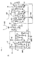
- FIG. 1 shows the circuit configuration of a duplexer 31 in a communication apparatus.
- FIG. 2 is a perspective view of the duplexer 31 in which the respective components are mounted onto a circuit substrate 40.
- a transmission side circuit 25 is electrically connected between a transmission terminal TX and an antenna terminal ANT, and a reception side circuit 26 between a reception terminal Rx and the antenna terminal ANT.
- the transmission side circuit 25 includes a frequency variable band elimination filter circuit 27 and a phase circuit 29.
- the frequency variable band elimination filter circuit 27 comprises resonant circuits in two stages coupled to each other, that is, it comprises a resonator 2 electrically connected to the transmission side terminal Tx via a resonance capacitor C1, and a resonator 3 electrically connected to the phase circuit 29 via a resonance capacitor C2.
- the resonance capacitors C1 and C2 are capacitors for determining the rejection-band attenuation.
- the series resonant circuit comprising the resonator 2 and the resonance capacitor C1 is electrically connected to the series resonant circuit comprising the resonator 3 and the resonance capacitor C2 via a coupling coil L1. Further, capacitors C5 and C6 are electrically connected in parallel to these two series resonant circuits, respectively.
- the PIN diode D2 as a reactance element is electrically connected in parallel with the resonator 2 with the cathode being grounded.
- the PIN diode D3 is electrically connected via a band variable capacitor C4, in parallel with the resonator 3.
- the band variable capacitors C3 and C4 are capacitors for changing two attenuation extreme frequencies of the attenuation characteristic of the frequency variable band elimination filter circuit 27, respectively.
- a capacitor 24 is connected in parallel to the band variable capacitor C4.
- the phase circuit 29 is a T-shaped type circuit comprising a coil L20 electrically connected between the frequency variable band elimination filter circuit 27 and the antenna terminal ANT, a capacitor 15 electrically connected between the ground and the antenna terminal ANT, and a coil L21 electrically connected between the band-pass filter circuit 28 (described later) of the reception side circuit 26 and the antenna terminal ANT.
- the reception side circuit 26 contains the frequency variable band-pass filter circuit 28 and the phase circuit 29.
- the reception side circuit 26 of the first embodiment shares the phase circuit 29 with the transmission side circuit 25.
- the transmission side circuit 25 and the reception side circuit 26 include independent phase circuits, respectively.
- the frequency variable band-pass filter circuit 28 comprises a resonant-circuit in three stages coupled to each other, that is, it comprises a resonator 4 electrically connected to the phase circuit 29 via a resonance inductance L9, a resonator 6 electrically connected to the reception terminal Rx via a resonance inductance L10, and a resonator 5 electrically connected between the resonators 4 and 6 via coupling capacitors C11, C12, C13, and C14.
- a series circuit comprising a band variable capacitor C7 and a PIN diode D4 is electrically connected in parallel with the resonator 4.
- a series circuit comprising a band variable capacitor C8 and a PIN diode D5 is electrically connected in parallel with the resonator 5.
- a series circuit comprising a band variable capacitor C9 and a PIN diode D6 is electrically connected in parallel with the resonator 6.
- a voltage control terminal CONT1 is electrically connected to the intermediate node between the anode of the PIN diode D2 and the band-variable capacitor C3, via a control voltage supply resistance R1, a capacitor C22, and a choke coil L2.
- a voltage control terminal CONT2 is electrically connected to the intermediate node between the anode of the PIN diode D3 and the band variable capacitor 4, via a control voltage supply resistor R2, a capacitor C23, and a choke coil L3, is electrically connected to the intermediate node between the anode of the PIN diode D4 and the band variable capacitor C7, via the control voltage supply resistance R2, the capacitor C23, and a choke coil L6, is electrically connected to the intermediate node between the anode of the PIN diode D5 and the band variable capacitor C8, via the control voltage supply resistor R2, the capacitor C23, and a choke coil L7, and further is electrically connected to the intermediate node between the anode of the PIN diode D6 and
- dielectric resonators are used as the resonators 2 to 6, as shown in FIG. 3.
- FIG. 3 shows the resonator 2 as a typical example.
- the dielectric resonators 2 to 6 each comprise a cylindrical dielectric 21 made of a material with a high dielectric constant such as a TiO 2 type ceramic or the like, an outer conductor 22 formed on the outer peripheral surface of the cylindrical dielectric 21, and an inner conductor 23 formed on the inner wall of the cylindrical dielectric 21.
- the outer conductor 22 is electrically opened (separated) from the inner conductor 23 at one open-end 21a (hereinafter, referred to as an open-end face 21a) of the dielectric 21, and electrically short-circuited (conducting) to the inner conductor 23 at the other open-end face 21b (hereinafter, referred to as a short-circuited end face 21b).
- the series circuit comprising the band variable capacitor C3 and the PIN diode D2 is electrically connected in such a manner that one end of the band variable capacitor C3 is connected to the inner conductor 23 at the open-end face 21a, and the cathode of the PIN diode D2 is connected to the ground.
- the outer conductor 22 is connected to the ground.
- a transmission signal, input to the transmission terminal Tx from a transmission circuit system is output from the antenna terminal ANT via the transmission side circuit 25, while a reception signal input through the antenna terminal ANT is output to a reception circuit system via the reception side circuit 26.
- the trap frequency of the frequency variable band elimination filter circuit 27 in the transmission side circuit 25 is determined by the resonance frequency of a resonance system comprising the band variable capacitor C3, the resonance capacitor C1, and the resonator 2, and the resonance frequency of a resonance system comprising the band variable capacitor C4, the resonance capacitor C2, and the resonator 3.
- the PIN diodes D2 and D3 are in the on state, respectively.
- the band variable capacitors C3 and C4 are grounded via the PIN diodes D2 and D3, so that both of the attenuation extreme frequencies are decreased, and the pass-band of the transmission side circuit 25 becomes a LOW channel (1850 - 1880 MHz).
- the control voltages are 0V with no voltages being applied to the voltage control terminals CONT1 and CONT2, the PIN diodes D2 and D3 are in the off state, respectively.
- Negative voltages may be applied to the voltage control terminals CONT1 and CONT2, instead of applying the control voltages of 0 V, so that the PIN diodes D2 and D3 are in the off state.
- the band variable capacitors C3 and C4 become open, respectively, so that both of the two attenuation frequencies are increased, and the pass-band of the transmission side circuit 25 becomes a HIGH channel (1880 - 1910 MHz).
- the two different pass-band characteristics can be rendered by carrying out the voltage control to ground or open the band-variable capacitors C3 and C4.
- the pass frequency of the frequency variable band-pass filter circuit 28 in the reception side circuit 26 is determined by the resonance frequency of a resonance system comprising the band variable capacitor C7, the resonance inductance L9, and the resonator 4, the resonance frequency of a resonance system comprising the band variable capacitor C8 and the resonator 5, and the resonance frequency of a resonance system comprising the band variable capacitor C9, the resonance inductance L10, and the resonator 6.
- the PIN diodes D4, D5, and D6 are in the on state.
- the band variable capacitors C7, C8, and C9 are grounded via the PIN diodes D4, D5, and D6, respectively, and the pass frequency is decreased, whereby the pass band of the reception side circuit 26 becomes a LOW channel (1930-1960 MHz).
- This duplexer 31 is voltage-controlled in such a manner that the two pass bands, namely, the high and low pass bands, are changed over. That is, when the low frequency pass band is selected as a transmission band, the pass frequency of the reception side circuit 26 is decreased, and when the high frequency pass band is selected as the transmission band, the pass frequency of the reception side circuit 26 is increased. Thereby, the phase of the transmission side circuit 25 and that of the reception side circuit 26 can be ideally composed.
- the duplexer 31 is put into the reception wave standby state, by making the control voltage of the voltage control terminal CONT1 0 V and applying a positive voltage to the voltage control terminal CONT2 only. That is, the PIN diodes D4 to D6 of the reception side circuit 26 and the PIN diode D3 electrically connected to the antenna terminal ANT in the position nearer to the antenna terminal ANT than the PIN diode D2 in the transmission side circuit 25 during the reception wave standby are in the on state. Accordingly, the transmission side circuit 25 is allowed to have a high impedance in the reception frequency band of 1930 - 1960 MHz, and the insertion loss of the reception side circuit 26 can be suppressed.
- FIG. 4 is a graph showing the measurement results of the band-pass characteristic S32 and the reflection characteristic S22 (see FIG. 1) of the reception side circuit 26 obtained when a positive voltage is applied to the voltage control terminal CONT2 only.
- the insertion loss of the reception side circuit 26 was 3.5 dB.
- the PIN diode D3 is in the on state during the reception wave standby. Both of the PIN diodes D2 and D3 in the transmission side circuit 25 are not in the on state. Thus, the power consumption during the reception wave standby can be suppressed.
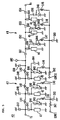
- FIG. 5 illustrates another embodiment of the duplexer of the present invention.
- a transmission side circuit 47 is electrically connected between a transmission terminal Tx and an antenna terminal ANT
- a reception side circuit 48 is electrically connected between a reception terminal Rx and the antenna terminal ANT.
- the transmission side circuit 47 is a frequency variable band elimination filter having resonant circuits in stages coupled together.
- a resonator 41 is electrically connected to a transmission terminal Tx via a resonance capacitor C41.
- a series resonant circuit comprising the resonator 41 and the resonance capacitor C41, a series resonant circuit comprising a resonator 42 and a resonance capacitor C42, and a series resonant circuit comprising a resonator 43 and a resonance capacitor C43 are electrically connected together via coupling coils L41 and L42.
- Capacitors C47, C48, and C49 are electrically connected in parallel to these three series resonant circuits, respectively.
- the antenna terminal ANT is electrically connected to the series resonant circuit comprising the resonator 43 and the resonance capacitor C43 via an L-LC circuit comprising a coupling coil L43 and a capacitor 50.
- the resonance capacitors C41 to C43 are capacitors for determining a rejection-band attenuation.
- a PIN diode D41 as a reactance element is electrically connected in parallel with the resonator 41 via band variable capacitor C44, with the cathode being grounded.
- a PIN diode D42 is electrically connected in parallel with the resonator 43 via a band variable capacitor C45.
- a PIN diode D43 is electrically connected in parallel with the resonator 43 via a band variable capacitor C46.
- the band variable capacitors C44 to C46 are capacitors for changing the attenuation extreme frequencies of the transmission side circuit 47.
- a capacitor 64 is connected in parallel to the band variable capacitor C46.
- the reception side circuit 48 is a frequency variable band-pass filter comprising resonant circuits in three stages connected together.
- a series resonant circuit comprising a resonator 44 and a resonance capacitor C55, a resonator 45, and a series resonant circuit comprising a resonator 46 and a resonance capacitor C56 are electrically connected via coupling capacitors C52 and C53. Further, the series resonant circuit comprising the resonator 44 and the resonance capacitor C55 is electrically connected to the antenna terminal ANT via a coupling capacitor C51. The series resonant circuit comprising the resonator 46 and the resonance capacitor C56 is electrically connected to the reception terminal Rx via a coupling capacitor C54.
- a series circuit comprising a band variable capacitor C57 and a PIN diode D44 is electrically connected in parallel with the resonator 44.
- a series circuit comprising a band variable capacitors C58 and C59, and the PIN diode D45 is electrically connected in parallel with the resonator 45.
- a series circuit comprising a band variable capacitor C60 and a PIN diode D46 is electrically connected in parallel with the resonator 46.
- a voltage control terminal CONT1 is electrically connected to the intermediate node between the anode of the PIN diode D41 and the band variable capacitor C44 via a control voltage supply resistor R41, a capacitor C62, and a choke coil L44, and is electrically connected to the intermediate node between the anode of the PIN diode D42 and the band variable capacitor C45 via the control voltage supply resistor R41, the capacitor C62, and a choke coil L45.
- a voltage control terminal CONT2 is electrically connected to the intermediate node between the anode of the PIN diode D43 and the band variable capacitor C46 via a control voltage supply resistor R42, a capacitor C63, and a choke coil L46, electrically connected to the intermediate node between the anode of the PIN diode D44 and the band variable capacitor C57 via the control voltage supply resistor R42, the capacitor C63, and a choke coil 47, and moreover, electrically connected to the intermediate node between the anode of the PIN diode D46 and the band variable capacitor C60 via the control voltage supply resistor R42, the capacitor C63, and a choke coil L49.
- the duplexer 40 having the above-described configuration has the same operation and effects as those of the duplexer 31 of the first embodiment.
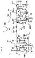
- FIG. 6 shows a duplexer according to a third embodiment of the present invention.
- a duplexer 70 is the same as the duplexer 40 of the second embodiment except that a voltage control terminal CONT3 for independently voltage-controlling the PIN diode D43, connected to the resonator 43 which is electrically connected to the antenna terminal ANT in the position nearest thereto in the transmission side circuit 47 is newly provided.
- the voltage control terminal CONT3 is connected to the intermediate node between the anode of the PIN diode D43 and the band variable capacitor C46 via a control voltage supply resistorR73, a capacitor C74, and a choke coil L46.
- the insertion loss of the respectively side circuit 48 is increased.
- the insertion loss of the reception side circuit 47 is deteriorated at about 1930 MHz only, which is near to the transmission frequency band (1850 - 1910 MHz), while substantially no deterioration of the insertion loss occurs near to 1960 MHz.
- the control voltages of the voltage control terminals CONT1 and CONT3 are made 0V and a positive voltage is applied to the voltage control terminal CONT2 only. That is, a consumption current is made to flow through the reception side circuit 48 only during reception wave standby.
- the control voltage of the voltage control terminal CONT1 is made 0V, and positive voltages are applied to the voltage control terminals CONT2 and CONT3. That is, during the reception wave standby, the PIN diodes D44 to D46, and the PIN diode D43 electrically connected in the position nearest to the antenna terminal ANT among the PIN diodes D41 to D43 in the transmission side circuit 47 are in the on state.
- the fourth embodiment will be described with reference to a portable telephone as an example of the communication apparatus of the present invention.
- FIG. 7 is an electric circuit block diagram of the RF part of a portable telephone 120.
- an antenna element is designated by 122, a duplexer by 123, a transmission side isolator by 131, a transmission side amplifier by 135, a reception side interstage band-pass filter by 136, a reception side mixer by 137, a voltage control oscillator (VCO) by 138, and a local band-pass filter by 139.
- VCO voltage control oscillator
- the duplexers 31, 40, and 70 of the first to third embodiments may be used.
- a portable telephone with a low power consumption and a low loss of the reception side circuit during reception wave standby can be realized by mounting the duplexer 31, 40, or 70.
- duplexer and the communication apparatus of the present invention are limited onto the above-described embodiments, and variations may be made without departing from the sprit and the scope of the present invention.
- the reactance element variable capacitance diodes, transistors or the like are available in addition to the PIN diode.
- the resonators strip line resonators or the like may be employed, in addition to the dielectric resonators.
Landscapes
- Engineering & Computer Science (AREA)
- Computer Networks & Wireless Communication (AREA)
- Signal Processing (AREA)
- Control Of Motors That Do Not Use Commutators (AREA)
- Transceivers (AREA)
- Filters And Equalizers (AREA)
Abstract
Description
Claims (8)
- A duplexer comprising:a first external terminal (TX);a second external terminal (RX);an antenna terminal (ANT);a first frequency variable filter (27; 47) electrically connected between the first external terminal (TX) and the antenna terminal (ANT), and composed of at least one resonator (3; 43) and a reactance element (D3; D43) electrically connected to the resonator (3; 43) and capable of being voltage-controlled;a second frequency variable filter (28; 48) electrically connected between the second external terminal (RX) and the antenna terminal (ANT), and composed of at least one resonator (4, 5, 6) and a reactance element (D4, D5, D6; D44, D45, D46) electrically connected to the resonator (4 - 6; 44 - 46) and capable of being voltage-controlled;the predetermined reactance element (D3; D43) of the first frequency variable filter (27; 47) being in the on state when the reactance element (D4 - D6; D44 - D46) of the second frequency variable filter (28; 48) is in the on state.
- A duplexer according to Claim 1, wherein the first frequency variable filter (27; 47) is a transmission filter, and the second frequency variable filter (28; 48) is a reception filter.
- A duplexer according to Claim 1 or 2, wherein the predetermined reactance element (D3; D43) of the first frequency variable filter (27; 47) is a reactance element connected to the resonator (3; 43) electrically connected in the position nearest to the antenna terminal (ANT).
- A duplexer according to one of Claims 1 to 3, further comprising a first voltage control terminal (CONT1) for voltage-controlling a reactance element (D2) other than the predetermined reactance element (D3) of the first frequency variable filter (27); anda second voltage control terminal (CONT2) for voltage-controlling the reactance element (D4 - D6) of the second frequency variable filter (28) and the predetermined reactance element (D3) of the first frequency variable filter (27).
- A duplexer according to one of Claims 1 to 3, further comprising a first voltage control terminal (CONT1) for voltage-controlling a reactance element (D41, D42) other than the predetermined reactance element (D43) of the first frequency variable filter (47);a second voltage control terminal (CONT3) for voltage-controlling the predetermined reactance element (D43) of the first frequency variable filter (47), anda third voltage control terminal (CONT2) for voltage-controlling a reactance element (D44 - D46) of the second frequency variable filter (48).
- A duplexer according to one of Claims 1 to 5, wherein the reactance element (D2 - D6; D41 - D46) is a PIN diode.
- A duplexer according to one of Claims 1 to 6, wherein the resonators (2 - 6; 41 - 46) constituting the first and second frequency variable filters (27, 28; 47, 48) are dielectric resonators.
- A communication apparatus including any one of the antenna devices of one of Claims 1 to 7.
Applications Claiming Priority (2)
| Application Number | Priority Date | Filing Date | Title |
|---|---|---|---|
| JP15710899 | 1999-06-03 | ||
| JP15710899A JP3475858B2 (en) | 1999-06-03 | 1999-06-03 | Antenna duplexer and communication device |
Publications (3)
| Publication Number | Publication Date |
|---|---|
| EP1058333A2 true EP1058333A2 (en) | 2000-12-06 |
| EP1058333A3 EP1058333A3 (en) | 2001-07-18 |
| EP1058333B1 EP1058333B1 (en) | 2006-11-22 |
Family
ID=15642415
Family Applications (1)
| Application Number | Title | Priority Date | Filing Date |
|---|---|---|---|
| EP00109460A Expired - Lifetime EP1058333B1 (en) | 1999-06-03 | 2000-05-03 | Duplexer and communication apparatus |
Country Status (5)
| Country | Link |
|---|---|
| US (1) | US6411176B1 (en) |
| EP (1) | EP1058333B1 (en) |
| JP (1) | JP3475858B2 (en) |
| KR (1) | KR100372154B1 (en) |
| DE (1) | DE60031912T2 (en) |
Cited By (3)
| Publication number | Priority date | Publication date | Assignee | Title |
|---|---|---|---|---|
| WO2002084781A1 (en) * | 2001-04-11 | 2002-10-24 | Kyocera Wireless Corporation | Tunable multiplexer |
| EP1291954A3 (en) * | 2001-08-27 | 2003-11-19 | Matsushita Electric Industrial Co., Ltd. | RF device and communication apparatus using the same |
| US6744327B2 (en) | 2001-04-11 | 2004-06-01 | Kyocera Wireless Corp. | Tunable voltage controlled oscillator |
Families Citing this family (20)
| Publication number | Priority date | Publication date | Assignee | Title |
|---|---|---|---|---|
| US6515559B1 (en) * | 1999-07-22 | 2003-02-04 | Matsushita Electric Industrial Co., Ltd | In-band-flat-group-delay type dielectric filter and linearized amplifier using the same |
| US7221243B2 (en) | 2001-04-11 | 2007-05-22 | Kyocera Wireless Corp. | Apparatus and method for combining electrical signals |
| US7174147B2 (en) | 2001-04-11 | 2007-02-06 | Kyocera Wireless Corp. | Bandpass filter with tunable resonator |
| US7154440B2 (en) | 2001-04-11 | 2006-12-26 | Kyocera Wireless Corp. | Phase array antenna using a constant-gain phase shifter |
| US7164329B2 (en) | 2001-04-11 | 2007-01-16 | Kyocera Wireless Corp. | Tunable phase shifer with a control signal generator responsive to DC offset in a mixed signal |
| US7394430B2 (en) | 2001-04-11 | 2008-07-01 | Kyocera Wireless Corp. | Wireless device reconfigurable radiation desensitivity bracket systems and methods |
| US7746292B2 (en) | 2001-04-11 | 2010-06-29 | Kyocera Wireless Corp. | Reconfigurable radiation desensitivity bracket systems and methods |
| US7071776B2 (en) | 2001-10-22 | 2006-07-04 | Kyocera Wireless Corp. | Systems and methods for controlling output power in a communication device |
| US7180467B2 (en) | 2002-02-12 | 2007-02-20 | Kyocera Wireless Corp. | System and method for dual-band antenna matching |
| US7176845B2 (en) | 2002-02-12 | 2007-02-13 | Kyocera Wireless Corp. | System and method for impedance matching an antenna to sub-bands in a communication band |
| US7184727B2 (en) | 2002-02-12 | 2007-02-27 | Kyocera Wireless Corp. | Full-duplex antenna system and method |
| US7720443B2 (en) | 2003-06-02 | 2010-05-18 | Kyocera Wireless Corp. | System and method for filtering time division multiple access telephone communications |
| US20050206482A1 (en) * | 2004-03-17 | 2005-09-22 | Dutoit Nicolaas | Electronically tunable switched-resonator filter bank |
| US7248845B2 (en) | 2004-07-09 | 2007-07-24 | Kyocera Wireless Corp. | Variable-loss transmitter and method of operation |
| WO2006071005A1 (en) | 2004-12-31 | 2006-07-06 | Kmw Inc. | Apparatus for using a wireless communication base station in common |
| DE102005050630A1 (en) * | 2005-10-21 | 2007-04-26 | Rohde & Schwarz Gmbh & Co. Kg | Switchable diplexer for microwave applications, has transverse units formed as switching units in highpass filter path and in lowpass filter path, making selective connection to ground |
| US7548762B2 (en) | 2005-11-30 | 2009-06-16 | Kyocera Corporation | Method for tuning a GPS antenna matching network |
| KR100859558B1 (en) * | 2006-02-28 | 2008-09-23 | 주식회사 케이엠더블유 | Wireless communication base station common device |
| JP4702178B2 (en) * | 2006-05-19 | 2011-06-15 | ソニー株式会社 | Semiconductor coupling device, semiconductor element, and high-frequency module |
| US9325353B2 (en) * | 2011-09-16 | 2016-04-26 | Rf Micro Devices, Inc. | Architecture for a radio frequency front-end |
Family Cites Families (8)
| Publication number | Priority date | Publication date | Assignee | Title |
|---|---|---|---|---|
| US4097826A (en) | 1975-06-30 | 1978-06-27 | Epsilon Lambda Electronics Corp. | Insular waveguide ring resonator filter |
| JPS57166701A (en) | 1981-04-03 | 1982-10-14 | Shigeo Nishida | Dielectric line |
| JPS639303A (en) * | 1986-06-30 | 1988-01-16 | Murata Mfg Co Ltd | Microwave filter and transmitting/receiving equipment using same |
| JP3208550B2 (en) | 1992-07-24 | 2001-09-17 | 本田技研工業株式会社 | Non-radiative dielectric line |
| US5594394A (en) * | 1993-08-31 | 1997-01-14 | Matsushita Electric Industrial Co., Ltd. | Antenna diversity switching device with switching circuits between the receiver terminal and each antenna |
| DE69834679T2 (en) * | 1997-03-12 | 2006-09-21 | Matsushita Electric Industrial Co., Ltd., Kadoma | antenna Combiner |
| JPH1146102A (en) * | 1997-05-30 | 1999-02-16 | Murata Mfg Co Ltd | Dielectric filter, dielectric duplexer and communication equipment |
| JPH11122139A (en) * | 1997-10-17 | 1999-04-30 | Murata Mfg Co Ltd | Antenna multicoupler |
-
1999
- 1999-06-03 JP JP15710899A patent/JP3475858B2/en not_active Expired - Fee Related
-
2000
- 2000-05-03 DE DE60031912T patent/DE60031912T2/en not_active Expired - Lifetime
- 2000-05-03 EP EP00109460A patent/EP1058333B1/en not_active Expired - Lifetime
- 2000-06-02 KR KR10-2000-0030336A patent/KR100372154B1/en not_active Expired - Fee Related
- 2000-06-05 US US09/587,505 patent/US6411176B1/en not_active Expired - Lifetime
Cited By (6)
| Publication number | Priority date | Publication date | Assignee | Title |
|---|---|---|---|---|
| WO2002084781A1 (en) * | 2001-04-11 | 2002-10-24 | Kyocera Wireless Corporation | Tunable multiplexer |
| US6744327B2 (en) | 2001-04-11 | 2004-06-01 | Kyocera Wireless Corp. | Tunable voltage controlled oscillator |
| CN1294673C (en) * | 2001-04-11 | 2007-01-10 | 基奥赛拉无线公司 | Tuning multiplexer |
| KR100798616B1 (en) * | 2001-04-11 | 2008-01-28 | 키오세라 와이어리스 코포레이션 | Tuned Multiplexer |
| EP1291954A3 (en) * | 2001-08-27 | 2003-11-19 | Matsushita Electric Industrial Co., Ltd. | RF device and communication apparatus using the same |
| US6985712B2 (en) | 2001-08-27 | 2006-01-10 | Matsushita Electric Industrial Co., Ltd. | RF device and communication apparatus using the same |
Also Published As
| Publication number | Publication date |
|---|---|
| DE60031912T2 (en) | 2007-04-05 |
| EP1058333A3 (en) | 2001-07-18 |
| JP3475858B2 (en) | 2003-12-10 |
| JP2000349509A (en) | 2000-12-15 |
| US6411176B1 (en) | 2002-06-25 |
| KR100372154B1 (en) | 2003-02-14 |
| EP1058333B1 (en) | 2006-11-22 |
| DE60031912D1 (en) | 2007-01-04 |
| KR20010007198A (en) | 2001-01-26 |
Similar Documents
| Publication | Publication Date | Title |
|---|---|---|
| EP1058333B1 (en) | Duplexer and communication apparatus | |
| KR100303638B1 (en) | Antenna Duplexer | |
| US6111482A (en) | Dielectric variable-frequency filter having a variable capacitance connected to a resonator | |
| US6522220B2 (en) | Frequency variable filter, antenna duplexer, and communication apparatus incorporating the same | |
| JP3454163B2 (en) | Variable frequency filter, antenna duplexer and communication device | |
| JP3473490B2 (en) | Antenna duplexer and communication device | |
| EP0993063A2 (en) | Duplexer and communication apparatus | |
| KR100327534B1 (en) | duplexer and communication apparatus | |
| KR100344925B1 (en) | Filter, antenna sharing device, and communication device | |
| JP3329278B2 (en) | Variable frequency filter, duplexer and communication device | |
| JPH11243304A (en) | Antenna duplexer | |
| JP3610924B2 (en) | Antenna duplexer and communication device | |
| JP2000013280A (en) | Dual band compatible antenna switch | |
| JP2000357905A (en) | Frequency variable resonance circuit, frequency variable filter, antenna-sharing device and communication device | |
| KR100273636B1 (en) | Apparatus for separating transmitting signal and receiving signal | |
| JP2002141707A (en) | Filter, antenna multicoupler and communication device | |
| JP2000114814A (en) | Frequency variable filter, antenna sharing device and communication equipment device | |
| JP2001217744A (en) | Composite high frequency circuit | |
| JPH11112207A (en) | High frequency circuit | |
| JPH0758520A (en) | Dielectric duplexer |
Legal Events
| Date | Code | Title | Description |
|---|---|---|---|
| PUAI | Public reference made under article 153(3) epc to a published international application that has entered the european phase |
Free format text: ORIGINAL CODE: 0009012 |
|
| 17P | Request for examination filed |
Effective date: 20000503 |
|
| AK | Designated contracting states |
Kind code of ref document: A2 Designated state(s): DE FR GB |
|
| AX | Request for extension of the european patent |
Free format text: AL;LT;LV;MK;RO;SI |
|
| PUAL | Search report despatched |
Free format text: ORIGINAL CODE: 0009013 |
|
| AK | Designated contracting states |
Kind code of ref document: A3 Designated state(s): AT BE CH CY DE DK ES FI FR GB GR IE IT LI LU MC NL PT SE |
|
| AX | Request for extension of the european patent |
Free format text: AL;LT;LV;MK;RO;SI |
|
| AKX | Designation fees paid |
Free format text: DE FR GB |
|
| GRAP | Despatch of communication of intention to grant a patent |
Free format text: ORIGINAL CODE: EPIDOSNIGR1 |
|
| GRAS | Grant fee paid |
Free format text: ORIGINAL CODE: EPIDOSNIGR3 |
|
| GRAA | (expected) grant |
Free format text: ORIGINAL CODE: 0009210 |
|
| AK | Designated contracting states |
Kind code of ref document: B1 Designated state(s): DE FR GB |
|
| REG | Reference to a national code |
Ref country code: GB Ref legal event code: FG4D |
|
| REF | Corresponds to: |
Ref document number: 60031912 Country of ref document: DE Date of ref document: 20070104 Kind code of ref document: P |
|
| ET | Fr: translation filed | ||
| RAP2 | Party data changed (patent owner data changed or rights of a patent transferred) |
Owner name: MURATA MANUFACTURING CO., LTD. |
|
| PLBE | No opposition filed within time limit |
Free format text: ORIGINAL CODE: 0009261 |
|
| STAA | Information on the status of an ep patent application or granted ep patent |
Free format text: STATUS: NO OPPOSITION FILED WITHIN TIME LIMIT |
|
| 26N | No opposition filed |
Effective date: 20070823 |
|
| REG | Reference to a national code |
Ref country code: FR Ref legal event code: PLFP Year of fee payment: 16 |
|
| PGFP | Annual fee paid to national office [announced via postgrant information from national office to epo] |
Ref country code: GB Payment date: 20150429 Year of fee payment: 16 Ref country code: DE Payment date: 20150428 Year of fee payment: 16 |
|
| PGFP | Annual fee paid to national office [announced via postgrant information from national office to epo] |
Ref country code: FR Payment date: 20150508 Year of fee payment: 16 |
|
| REG | Reference to a national code |
Ref country code: DE Ref legal event code: R119 Ref document number: 60031912 Country of ref document: DE |
|
| GBPC | Gb: european patent ceased through non-payment of renewal fee |
Effective date: 20160503 |
|
| REG | Reference to a national code |
Ref country code: FR Ref legal event code: ST Effective date: 20170131 |
|
| PG25 | Lapsed in a contracting state [announced via postgrant information from national office to epo] |
Ref country code: DE Free format text: LAPSE BECAUSE OF NON-PAYMENT OF DUE FEES Effective date: 20161201 Ref country code: FR Free format text: LAPSE BECAUSE OF NON-PAYMENT OF DUE FEES Effective date: 20160531 |
|
| PG25 | Lapsed in a contracting state [announced via postgrant information from national office to epo] |
Ref country code: GB Free format text: LAPSE BECAUSE OF NON-PAYMENT OF DUE FEES Effective date: 20160503 |