EP1057382B1 - High frequency electronic ballast for multiple lamp independent operation - Google Patents
High frequency electronic ballast for multiple lamp independent operation Download PDFInfo
- Publication number
- EP1057382B1 EP1057382B1 EP99965486A EP99965486A EP1057382B1 EP 1057382 B1 EP1057382 B1 EP 1057382B1 EP 99965486 A EP99965486 A EP 99965486A EP 99965486 A EP99965486 A EP 99965486A EP 1057382 B1 EP1057382 B1 EP 1057382B1
- Authority
- EP
- European Patent Office
- Prior art keywords
- voltage
- ballast
- coupled
- lamps
- output
- Prior art date
- Legal status (The legal status is an assumption and is not a legal conclusion. Google has not performed a legal analysis and makes no representation as to the accuracy of the status listed.)
- Expired - Lifetime
Links
- 239000003990 capacitor Substances 0.000 claims description 21
- 230000010363 phase shift Effects 0.000 claims description 15
- 230000004044 response Effects 0.000 claims description 11
- 230000008859 change Effects 0.000 claims description 10
- 230000007704 transition Effects 0.000 claims description 10
- 238000004804 winding Methods 0.000 claims description 8
- 238000010438 heat treatment Methods 0.000 claims description 2
- 230000008878 coupling Effects 0.000 claims 1
- 238000010168 coupling process Methods 0.000 claims 1
- 238000005859 coupling reaction Methods 0.000 claims 1
- 230000001143 conditioned effect Effects 0.000 description 9
- 238000000034 method Methods 0.000 description 6
- 238000010586 diagram Methods 0.000 description 5
- 230000001965 increasing effect Effects 0.000 description 5
- 238000007493 shaping process Methods 0.000 description 5
- 230000000694 effects Effects 0.000 description 4
- 230000008569 process Effects 0.000 description 3
- 230000001105 regulatory effect Effects 0.000 description 3
- 230000008901 benefit Effects 0.000 description 2
- 230000033228 biological regulation Effects 0.000 description 2
- 230000000903 blocking effect Effects 0.000 description 2
- 230000007423 decrease Effects 0.000 description 2
- 238000002955 isolation Methods 0.000 description 2
- 239000004065 semiconductor Substances 0.000 description 2
- 230000001276 controlling effect Effects 0.000 description 1
- 230000006378 damage Effects 0.000 description 1
- 230000003247 decreasing effect Effects 0.000 description 1
- 230000001419 dependent effect Effects 0.000 description 1
- 230000001939 inductive effect Effects 0.000 description 1
- 238000004519 manufacturing process Methods 0.000 description 1
- 238000012544 monitoring process Methods 0.000 description 1
- 238000010408 sweeping Methods 0.000 description 1
Images




Classifications
-
- H—ELECTRICITY
- H02—GENERATION; CONVERSION OR DISTRIBUTION OF ELECTRIC POWER
- H02M—APPARATUS FOR CONVERSION BETWEEN AC AND AC, BETWEEN AC AND DC, OR BETWEEN DC AND DC, AND FOR USE WITH MAINS OR SIMILAR POWER SUPPLY SYSTEMS; CONVERSION OF DC OR AC INPUT POWER INTO SURGE OUTPUT POWER; CONTROL OR REGULATION THEREOF
- H02M7/00—Conversion of AC power input into DC power output; Conversion of DC power input into AC power output
- H02M7/42—Conversion of DC power input into AC power output without possibility of reversal
- H02M7/44—Conversion of DC power input into AC power output without possibility of reversal by static converters
- H02M7/48—Conversion of DC power input into AC power output without possibility of reversal by static converters using discharge tubes with control electrode or semiconductor devices with control electrode
- H02M7/53—Conversion of DC power input into AC power output without possibility of reversal by static converters using discharge tubes with control electrode or semiconductor devices with control electrode using devices of a triode or transistor type requiring continuous application of a control signal
- H02M7/537—Conversion of DC power input into AC power output without possibility of reversal by static converters using discharge tubes with control electrode or semiconductor devices with control electrode using devices of a triode or transistor type requiring continuous application of a control signal using semiconductor devices only, e.g. single switched pulse inverters
- H02M7/538—Conversion of DC power input into AC power output without possibility of reversal by static converters using discharge tubes with control electrode or semiconductor devices with control electrode using devices of a triode or transistor type requiring continuous application of a control signal using semiconductor devices only, e.g. single switched pulse inverters in a push-pull configuration
- H02M7/53803—Conversion of DC power input into AC power output without possibility of reversal by static converters using discharge tubes with control electrode or semiconductor devices with control electrode using devices of a triode or transistor type requiring continuous application of a control signal using semiconductor devices only, e.g. single switched pulse inverters in a push-pull configuration with automatic control of output voltage or current
-
- H—ELECTRICITY
- H05—ELECTRIC TECHNIQUES NOT OTHERWISE PROVIDED FOR
- H05B—ELECTRIC HEATING; ELECTRIC LIGHT SOURCES NOT OTHERWISE PROVIDED FOR; CIRCUIT ARRANGEMENTS FOR ELECTRIC LIGHT SOURCES, IN GENERAL
- H05B41/00—Circuit arrangements or apparatus for igniting or operating discharge lamps
- H05B41/14—Circuit arrangements
- H05B41/26—Circuit arrangements in which the lamp is fed by power derived from DC by means of a converter, e.g. by high-voltage DC
- H05B41/28—Circuit arrangements in which the lamp is fed by power derived from DC by means of a converter, e.g. by high-voltage DC using static converters
- H05B41/282—Circuit arrangements in which the lamp is fed by power derived from DC by means of a converter, e.g. by high-voltage DC using static converters with semiconductor devices
- H05B41/2825—Circuit arrangements in which the lamp is fed by power derived from DC by means of a converter, e.g. by high-voltage DC using static converters with semiconductor devices by means of a bridge converter in the final stage
- H05B41/2828—Circuit arrangements in which the lamp is fed by power derived from DC by means of a converter, e.g. by high-voltage DC using static converters with semiconductor devices by means of a bridge converter in the final stage using control circuits for the switching elements
-
- H—ELECTRICITY
- H05—ELECTRIC TECHNIQUES NOT OTHERWISE PROVIDED FOR
- H05B—ELECTRIC HEATING; ELECTRIC LIGHT SOURCES NOT OTHERWISE PROVIDED FOR; CIRCUIT ARRANGEMENTS FOR ELECTRIC LIGHT SOURCES, IN GENERAL
- H05B41/00—Circuit arrangements or apparatus for igniting or operating discharge lamps
- H05B41/14—Circuit arrangements
- H05B41/26—Circuit arrangements in which the lamp is fed by power derived from DC by means of a converter, e.g. by high-voltage DC
- H05B41/28—Circuit arrangements in which the lamp is fed by power derived from DC by means of a converter, e.g. by high-voltage DC using static converters
- H05B41/295—Circuit arrangements in which the lamp is fed by power derived from DC by means of a converter, e.g. by high-voltage DC using static converters with semiconductor devices and specially adapted for lamps with preheating electrodes, e.g. for fluorescent lamps
- H05B41/298—Arrangements for protecting lamps or circuits against abnormal operating conditions
- H05B41/2981—Arrangements for protecting lamps or circuits against abnormal operating conditions for protecting the circuit against abnormal operating conditions
- H05B41/2986—Arrangements for protecting lamps or circuits against abnormal operating conditions for protecting the circuit against abnormal operating conditions against internal abnormal circuit conditions
-
- H—ELECTRICITY
- H05—ELECTRIC TECHNIQUES NOT OTHERWISE PROVIDED FOR
- H05B—ELECTRIC HEATING; ELECTRIC LIGHT SOURCES NOT OTHERWISE PROVIDED FOR; CIRCUIT ARRANGEMENTS FOR ELECTRIC LIGHT SOURCES, IN GENERAL
- H05B41/00—Circuit arrangements or apparatus for igniting or operating discharge lamps
- H05B41/14—Circuit arrangements
- H05B41/36—Controlling
- H05B41/38—Controlling the intensity of light
- H05B41/39—Controlling the intensity of light continuously
- H05B41/392—Controlling the intensity of light continuously using semiconductor devices, e.g. thyristor
- H05B41/3921—Controlling the intensity of light continuously using semiconductor devices, e.g. thyristor with possibility of light intensity variations
- H05B41/3925—Controlling the intensity of light continuously using semiconductor devices, e.g. thyristor with possibility of light intensity variations by frequency variation
-
- Y—GENERAL TAGGING OF NEW TECHNOLOGICAL DEVELOPMENTS; GENERAL TAGGING OF CROSS-SECTIONAL TECHNOLOGIES SPANNING OVER SEVERAL SECTIONS OF THE IPC; TECHNICAL SUBJECTS COVERED BY FORMER USPC CROSS-REFERENCE ART COLLECTIONS [XRACs] AND DIGESTS
- Y02—TECHNOLOGIES OR APPLICATIONS FOR MITIGATION OR ADAPTATION AGAINST CLIMATE CHANGE
- Y02B—CLIMATE CHANGE MITIGATION TECHNOLOGIES RELATED TO BUILDINGS, e.g. HOUSING, HOUSE APPLIANCES OR RELATED END-USER APPLICATIONS
- Y02B70/00—Technologies for an efficient end-user side electric power management and consumption
- Y02B70/10—Technologies improving the efficiency by using switched-mode power supplies [SMPS], i.e. efficient power electronics conversion e.g. power factor correction or reduction of losses in power supplies or efficient standby modes
-
- Y—GENERAL TAGGING OF NEW TECHNOLOGICAL DEVELOPMENTS; GENERAL TAGGING OF CROSS-SECTIONAL TECHNOLOGIES SPANNING OVER SEVERAL SECTIONS OF THE IPC; TECHNICAL SUBJECTS COVERED BY FORMER USPC CROSS-REFERENCE ART COLLECTIONS [XRACs] AND DIGESTS
- Y10—TECHNICAL SUBJECTS COVERED BY FORMER USPC
- Y10S—TECHNICAL SUBJECTS COVERED BY FORMER USPC CROSS-REFERENCE ART COLLECTIONS [XRACs] AND DIGESTS
- Y10S315/00—Electric lamp and discharge devices: systems
- Y10S315/07—Starting and control circuits for gas discharge lamp using transistors
Definitions
- This invention relates to an electronic ballast for driving a set of gas discharge lamps which is capable of driving the lamps independently of lamp loading, i.e., with less than all of the lamps in the set connected or operating, and in a transition period during which a lamp already connected stops or starts operating, or a during which a lamp is changed.
- Electronic ballasts may include a resonant inverter which is current-fed or voltage-fed.
- the invention herein relates to an electronic ballast with a voltage-fed resonant inverter.
- Electronic ballasts that drive a set of gas discharge lamps should regulate the output to the lamps to drive the lamps with all, or less than all, of the lamps in the set operating or connected. Thus, if a lamp either degrades, stops lighting altogether or is disconnected, the ballast should continue to provide a satisfactory output to the remaining operating lamps. The same applies in a transition period during which a lamp already connected stops or starts operating and when a lamp is changed. It is highly desirable for a ballast to continue operating the remaining lamps connected thereto during a lamp change and to ignite a newly connected lamp so that it is not necessary to turn the power off to the ballast during lamp changing or to restart all of the lamps after a lamp change.
- electronic ballasts for multiple lamp operation advantageously should operate all connected lamps independently of lamp loading as indicated above. Such ballasts advantageously should also permit instant and/or rapid start operation.
- An electronic ballast with a current-fed inverter requires a large, heavy inductor in series with the input of the inverter.
- Such ballasts are less affected by lamp loading due largely to the presence of the large input inductor, and are capable of multiple lamp operation independently of lamp loading,
- the large input inductor required by current-fed inverters increases the cost and the size and weight of the ballast.
- U.S. Patent No. 5,519,289 discloses an electronic ballast for multiple lamp operation with dimming, which includes a push-pull, self-oscillating inverter.
- U.S. Patent 5,438,243 discloses an electronic ballast for multiple independent lamp operation of instant start gas discharge lamps, which includes a quasi-voltage-fed half-bridge parallel resonant inverter, as shown in Fig. 2 of the patent.
- the electronic ballast operates in current-fed parallel resonant mode where the current source is derived from an ideal voltage source in series with a first resonant tank circuit.
- a second resonant circuit is provided in order to maintain a high voltage output for lamp starting, which requires a high Q.
- the electronic ballast circuit disclosed in this patent thus contains two cascaded resonant tanks. As a result, circuit losses and cost are increased.
- ballast inductors are provided in series with two lamps and two ballast capacitors are provided in series with two other lamps, which reduces the reactive power requirement on the secondary side of the output transformer.
- this electronic ballast may impose a high voltage hazard across the output terminals when the lamps are removed while the circuit is hot.
- Other types of electronic ballast circuits with current-fed push-pull or half-bridge inverters for multiple florescent lamps are described at pages 583 and 584 of Power Semiconductor Applications Handbook 1995 , Philips Semiconductor, 1994.
- each lamp is parallel connected to the output of a resonant inverter via a series ballast capacitor.
- the current source is usually obtained via a choke inductor in series with a voltage source. Good independent lamp operation is achieved via a constant relation between the output high frequency voltage and the input DC voltage.
- the disadvantages of this type of circuit include higher switch stresses and the added bulky choke inductor.
- an electronic ballast with a voltage-fed resonant inverter including well known half-bridge LC or LLC resonant inverters, do not require a large input inductor but are affected more by lamp loading, and thus require additional circuitry or resonant components in order to achieve multiple lamp independent operation.
- U.S. Patents Nos. 5,438,243, 5,394,064, 5,075,599 and 4,535,399 disclose electronic ballasts for multiple lamp independent operation which include voltage fed inverters.
- the electronic ballast described in U.S. Patent No. 5,394,064, which permits dimming operation, includes a voltage-fed half-bridge resonant inverter which generates a high frequency square-wave voltage. Control is provided by varying the input voltage to the inverter or the inverter frequency, or both using voltage feedback from the input to the inverter and feedback from the lamp circuit to the oscillator driving the inverter switches. As shown in Fig.
- a transformer couples the lamps to the inverter, with each lamp being driven through an individual resonant tank circuit consisting of a series inductor and a parallel capacitor.
- the circuit for connecting the lamps may be considered as a parallel connection of multiple resonant tanks each loaded with a single lamp.
- the electronic ballast described in U.S. Patent No. 4,535,399 includes a voltage-fed resonant inverter and a separate resonant tank circuit for each lamp (Fig. 6).
- Each of the separate resonant tank circuits includes a small inductor and a capacitor, which adds to the cost of the ballast.
- This ballast also includes a current feedback loop which controls switching of a pulse width modulator (“PWM”) that supplies the timing for driving the inverter.
- PWM pulse width modulator
- the current feedback loop includes a phase locked loop (“PLL”) which provides a DC output to the PWM proportional to the change in phase of the current sensed at the output of the inverter.
- the PLL forces the inverter to operate at a frequency where the modulating pulses are initiated at the load current zero crossing.
- the PLL includes a low pass filter (Fig. 2) and has a suitable low frequency response which allows the PLL to maintain tracking during steady state operation.
- the PLL has a poor high frequency response which prevents the PLL from tracking fast transients that are produced, for example, when a lamp is disconnected or connected. As a result, the PLL may cease tracking, i.e., become unlocked during a lamp change, which can cause loss of zero voltage switching and destruction of the inverter.
- U.S. Patents Nos. 5,075,599 and 4,277,728 both disclose electronic ballasts for driving a single gas discharge lamp with a phase related feedback loop for control.
- correction towards a target phase angle difference e.g., 0
- a minimum reference phase angle difference is less the measured phase angle difference (Fig. 5). If the measured phase angle difference is greater than reference phase angle difference, then no correction is made.
- a phase detector Figs. 4a and 4b
- senses the phase difference between the input to the inverter pushh-pull in Fig. 4a and half-bridge in Fig. 4b
- the phase difference should be 90 degrees, indicating that the inverter is operating at the resonant frequency. If the phase difference is not 90 degrees, the phase detector provides an error signal causing the inverter to change frequency towards the resonant frequency.
- the electronic ballast disclosed in the '728 patent also includes an inductor in the resonant circuit which limits current to the load.
- DE-A-19805732 discloses a ballast circuit for a discharge lamp comprising a feedback loop for regulating the lamp power by maintaining the phase angle between the load current and the load voltage at a predetermined value.
- DE-A-19805733 discloses an electronic ballast for multiple lamp operation comprising such a feedback loop.
- the inventors found that the voltage gain of a voltage-fed, half-bridge resonant inverter remains almost constant if the phase angle • in , defined as the phase difference between the voltage V in and the current I LR in the tank circuit (e.g., see Fig. 4) is used as the direct control variable and maintained constant, even during a transition period when a lamp is extinguished, ignited, disconnected or connected.
- Fig. 2 illustrates the phase angle • in vs the switching frequency (f) relationship for a lamp load of m (1-4) lamps.
- Fig. 3 shows the relationship between the voltage gain (V gain ) and the phase angle (• in ) for a lamp load of m (1-4) lamps.
- the voltage gain curves are merged into a small band, especially in the higher frequency region. This closeness indicates that for a given phase angle • in , the voltage gain is almost independent of the number of lamps. During lamp transitions, if the phase angle • in is kept fixed or is allowed to change slightly, the output voltage V 0 is almost constant. As a result, multiple independent lamp operation can be achieved even during lamp change or lamp operation transitions.
- the phase angle • in and the voltage gain V gain are inversely related, with the voltage gain decreasing with increasing phase angle.
- this relationship is used for dimming operation of a single rapid start lamp or a set of rapid start lamps. Specifically, changing the phase angle in response to a command level signal will dim or brighten a lamp connected to the ballast.
- the inverse relationship of voltage gain and phase angle plotted in Fig. 3 applies regardless of the number of lamps connected to the ballast.
- the lighting level of one or of a set of rapid start lamps is controlled independently of the number of lamps connected by varying the phase angle.
- the invention achieves the above objects by providing an electronic ballast which includes a voltage-fed half-bridge resonant inverter, and control and feedback circuitry coupled to the inverter so as to maintain a substantially constant phase angle between the voltage and the current in an LC or LLC tank circuit, which has the effect of the ballast providing the substantially constant voltage output.
- the response of the control and feedback circuitry is such that the loop continues tracking when a lamp is extinguished, ignited, disconnected or connected.
- controlling the inverter to provide an AC output with a constant phase angle has the effect of providing a substantially constant voltage output to the lamps independently of lamp loading.
- such control and feedback circuitry uses a phase-shift technique that does not employ a phase locked loop.
- control and feedback circuitry includes a controller and a feedback loop.
- the feedback loop obtains a current feedback signal and a voltage feedback signal from the tank circuit, and provides a phase shifted signal as a feedback correction signal to the controller.
- the phase shifted signal which is the current feedback signal conditioned by the voltage feedback signal, tracks phase angle changes with one, some or all of the lamps of a set thereof connected to the ballast, and during a transition period in which a lamp is ignited, extinguished, disconnected or connected.
- the feedback loop includes a phase-shift circuit which includes at least one differential amplifier stage that receives the current feedback signal at both inputs and the voltage feedback signal at one input so as to phase shift the current feedback signal and provide the phase-shifted correction signal at the output of the at least one differential amplifier stage.
- This feedback loop and the controller cause the inverter to provide an AC output with substantially constant phase angle even when a lamp is extinguished, ignited, disconnected or connected.
- varying the phase angle in response to a command signal provides for dimming operation of rapid start lamps.
- the controller includes a pulse width modulation (PWM) control circuit which receives the phase shift correction signal in the feedback loop and provides drive signals that are coupled to the inverter to provide an output to the lamps with a substantially constant phase angle.
- PWM pulse width modulation
- the phase-shift circuit in the feedback loop provides the phase shift correction signal to the PWM control circuit in response to the current and voltage sensed in the resonant tank circuit coupled to the output of the inverter.
- the lamps are coupled in parallel to the tank circuit via a transformer, and a small ballast capacitor is coupled in series with each lamp. No inductive ballast components are required.
- the electronic ballast may also utilize the feedback loop to sense an overvoltage condition in the tank circuit, in response to which the controller stops operation of the inverter, i.e., stops supplying the inverter with drive signals.
- the inventive electronic ballast operates instant start and rapid start lamps with generally the same circuit configuration on the primary side of the output transformer.
- the output transformer secondary includes a portion coupled as a filament heater for each lamp, and the resonant inductor in the tank circuit has secondaries coupled to the filament of each lamp for steady state operation.
- the feedback loop tracks during lamp warm-up and ignition.
- the inventive electronic ballast operates multiple lamps in a parallel configuration and in a parallel/series configuration.
- the inventive electronic ballast may be used in dimming applications for multiple rapid start lamps in various series and parallel lamp configurations.
- the inventive electronic ballast 10 includes a voltage-fed half-bridge resonant inverter 12, an LC resonant tank circuit 14, and control and feedback circuitry including a controller 16 and a feedback loop 18 to the controller 16.
- An overvoltage feedback loop 20 is also provided to the controller 16.
- the feedback loop 18 performs current and voltage sensing, phase shifting and with the controller 16 provides drive signals at 22, 23 to the inverter 12 to maintain the phase angle • in constant.
- the feedback loop 20 performs voltage sensing and operates with the controller 16 to discontinue drive signals to the inverter 12 when an overvoltage condition is sensed.
- a DC voltage source Vbus feeds the inverter 12.
- An output isolation transformer T1 couples the resonant tank circuit 14 to multiple, instant start lamps 30.
- the lamps 30 are coupled to the electronic ballast by connectors, represented schematically by 32 and 33, and collectively present a variable load represented by R1 to the electronic ballast 10.
- the lamps 30 are coupled in parallel through respective ballast capacitors 35, represented collectively by C1.
- the feedback loop 18 includes a current sense portion 18a comprising a current sensor 40, a high pass filter 41 and an automatic gain control (AGC) circuit 42, and a voltage sense portion 18b comprising a voltage scaler 45 and a voltage compensator 46 circuit.
- the feedback loop 18 also includes a phase shifter 50 to which is coupled the current and voltage sense portions 18a and 18b.
- the current sense portion 18a senses the current in the resonant tank circuit 14 (current sensor 40) and provides an Isense signal, passes resonant frequency Isense signals (high pass filter 41), and maintains a suitable signal level (AGC circuit 42) of the high passes Isense signals, which are fed to the phase shifter 50.
- the voltage sense portion 18b couples the voltage at the output of the tank circuit 14 (Vsense signal) to the voltage scaler 45 which reduces the Vsense voltage to a suitable level and supplies the scaled voltage to a voltage compensator 46 which provides an output voltage to the phase shifter 50 proportional to the difference between the scaled Vsense tank output voltage and a reference voltage (V ref ).
- the conditioned Vsense signal of loop portion 18b provided by compensator 46 is supplied to the phase shifter 50 as a reference signal, and the conditioned Isense signal of the feedback loop portion 18a is provided by the AGC circuit 42 to the phase shifter 50 as the uncorrected phase angle signal.
- the phase shifter 50 provides a phase angle correction signal which is generally sinusoidal.
- the wave shaping circuit 55 converts the sinusoidal signal to square wave and supplies it to the controller 16 as the Phase-Shifted signal.
- the controller 16 illustrated in Fig. 4 includes a PWM control circuit 58, logic circuitry 60 and a gate driver 62.
- the output of wave shaping circuit 55 (Phase-Shifted signal) triggers the PWM control circuit 58 which outputs a PWM timing pulse to logic circuitry 60.
- Combinatorial logic circuitry 60 couples the PWM timing pulse or a Start-Up signal as a Gate Trigger signal to the gate driver 62, which supplies the drive signals at 22 and 23 to power switches 64 and 65 (Fig. 5) in the inverter 12 to alternately turn them on and off.
- a start-up circuit 63 is coupled to receive the DC input voltage (BusVsense) to the inverter 12 and provide the Start-Up signal to the logic circuitry 60 for igniting a set of extinguished lamps 30, e.g., when the ballast 10 is first turned on.
- the output voltage V o to the load is regulated to a constant value with from one to four lamps 30 connected, even during the transition periods when a lamp is extinguished or ignited.
- Such regulation of the ballast output voltage typically leads to a good crest factor of the lamp current.
- the overvoltage feedback loop 20 (Fig. 4) includes a voltage scaler 66 coupled to receive the tank output voltage (Vsense signal), and a flip-flop 67 coupled thereto which provides an OverVoltage signal to the logic circuitry 60, which then discontinues Gate Trigger signals to the gate driver circuit 62 to shut down the ballast as long as the overvoltage condition is present.
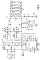
- Fig. 5 depicts details of the inverter 12, the gate driver 62, the current sense input to the feedback loop current portion 18a and the voltage sense input to the feedback loop voltage portion 18b.
- a DC voltage provided by a rectifier circuit 68 coupled to the AC line is supplied to the input to inverter 12.
- This DC signal coupled through one or more resistors, is supplied to the start-up circuit 63 (Figs. 4 and 8) as the Bus Vsense signal.
- the gate driver 62 may include an International Rectifier IR2111 half-bridge driver.
- the two power switches 64 and 65 in the inverter 12 provide a square wave output voltage to the tank circuit 14, which provides a sinusoidal voltage at the resonant frequency of the tank circuit to the primary of the transformer T1.
- the current sensor 40 comprises a resistor 69 connected in series with the return leg of the tank circuit 14 and a differential amplifier 70 coupled across the resistor 69.
- the output of the differential amplifier 70 provides the Isense signal which is coupled to the high pass filter 41 (Figs. 4 and 6). (Operation of certain components represented by operational amplifiers in Figs.
- the voltage sense loop portion 18b is coupled to the positive output of the tank circuit 14 through a rectifier diode 72 and a current limiting resistor or resistors 73, to provide the Vsense signal which is coupled to the voltage scaler 45 (Figs. 4 and 6).
- the high pass filter 41 receiving the Isense signal from Fig. 5 as its input, comprises a series capacitor 75 and a parallel resistor 76.
- the output of the high pass filter 41 is supplied to the AGC circuit 42 through two buffer stages 78 and 79.
- the output of the AGC circuit 42 (Conditioned Isense) is supplied to the phase shifter circuit 50 via another buffer stage 80.
- the Vsense signal from Fig. 5 is fed to the voltage scaler 45, which is coupled to the compensating circuit 46.
- the compensating circuit 46 includes a differential amplifier 82 which receives the output from the voltage scaler 45 on its inverting input and a reference voltage on its non-inverting input, and provides an output related to the difference between the scaled Vsense voltage and the reference voltage.
- the output of the compensator differential amplifier 82 is fed to a low pass filter and voltage limiter 87, the output of which (Conditioned Vsense) is fed to two JFET transistors 84, 85 functioning as variable resistors.
- the phase shifter 50 (Fig. 6) includes two stages 89, 90, each including a differential amplifier 91, 92.
- the inverting and non-inverting inputs of the first stage amplifier 91 receive the filtered, gain controlled current sense (Conditioned Isense) signal from buffer stage 80 via a resistor 94 and DC blocking capacitor 95, respectively.
- the first stage amplifier 91 also receives a variable reference signal from JFET 84 on its non-inverting input which shifts the phase of the conditioned current sense (Condition Isense) signal on the non-inverting input.
- the amount of shift is determined by the conductivity of the JFET 84, which is controlled by the input signal to its gate terminal provided by the output (Conditioned Vsense) of the compensator circuit 46.
- the output of the first stage amplifier 91 is proportional to the difference in the filtered, gain controlled current sense (Isense) signal and the shifted (by Conditioned Vsense), filtered, gain controlled current sense signal, where the amount of shift represents the phase difference between the current sense signal Isense and V in .
- the second stage differential amplifier 92 operates like the first stage differential amplifier 91 to provide extended phase shift range of the sensed circuit signal, via a voltage filter stage 93, which is supplied to the wave shaping circuit 55 (Figs. 4 and 7).
- Fig. 7 illustrates the circuit schematic diagram for the wave shaping circuit 55, the PWM control circuit 58, the start-up circuit 63 and part of the logic circuitry 60.
- the waveshaping circuit 55 includes a voltage buffer stage 95, which receives the Phase-Shifted signal from the voltage filter stage 93 in Fig. 6, and a comparator stage 97 which converts the buffered sinusoidal Phase-Shifted signal into a square wave signal.
- the PWM control circuit 58 includes a timing circuit 99 (e.g., Motorola MC1455), which receives the square wave Phase-Shifted signal from the comparator stage 97 as a trigger and provides a pulse (PWM Timing Pulse) at its output whose width is related to the Phase-Shifted signal.
- a timing circuit 99 e.g., Motorola MC1455
- the start-up circuit 63 includes a voltage-controlled oscillator (VCO) 102 (e.g., AD654 commercially available from known sources) in Fig. 7 and a sweep trigger circuit 104 in Fig. 8 which supplies the Sweep Trigger signal.
- VCO voltage-controlled oscillator
- the sweep trigger circuit 104 includes a simple voltage scaler 110, a comparator 110a, and a flip-flop 111.
- the scaler 110 receives the Bus Vsense signal (Figs. 4 and 5) from the input to the inverter 12, and provides the Sweep Trigger signal when the Bus Vsense signal exceeds a reference voltage as determined by comparator 110a.
- the flip-flop 111 clocked by the output of comparator 110a, maintains the Sweep Trigger signal until the Bus Vsense signal reaches the reference voltage coupled to comparator 110a.
- a minimal Bus Vsense signal is required before any lamp can be ignited.
- the Sweep Trigger signal turns transistor 112 (Fig. 7) off and allows capacitor 113 to charge, which creates an increasing ramp or sweep voltage to VCO 102.
- the width of the Sweep Trigger signal determines the range of frequencies of the signals output by the VCO 102 (pin 1).
- the voltage scaler 66 (Fig. 4) and the flip-flop 67 of the overvoltage feedback loop 20 are shown in detail in Fig. 8.
- the scaler 66 is implemented by a comparator 66a which clocks the flip-flop 67 to supply the OverVoltage signal as described above, i.e., whenever the Vsense signal exceeds the reference voltage to the comparator 66a.
- the OR gate 117 provides Gate Trigger signals from Trigger signals in the absence of an OverVoltage signal.
- FIG. 8 Another portion of the logic circuitry 60 in Fig. 8 provides a Loop Trigger signal, and includes a scaler circuit 115, implemented by a comparator 115a, and a flip-flop 116.
- the flip flop 116 provides the Loop Trigger signal whenever the Vsense signal exceeds a predetermined level, indicating that the lamp output level is proper.
- the Loop Trigger signal is supplied to OR gate 120 in Fig. 7, which provides a input signal to OR gate 121 if a PWM Timing pulse is present (from timer 118 indicating normal phase-shift controlled operation), or a Loop Trigger signal is present (flip-flop 116 in Fig. 8 indicating that the lamp output voltage is at a proper level).
- OR gate 121 (Fig.
- OR gate 120 provides an output (PWM Timing pulse or Loop Trigger), or if the start-up circuit 63 (Fig. 7) is providing swept frequencies (Start-Up signal) to the OR gate 122 with flip-flop 123 clocked by the output of OR gate 120.
- the Trigger signal is supplied to switch the ballast from the start-up (frequency sweeping) mode to steady state (Phase-Shift control) mode.
- the OR gate 117 (Fig. 8) passes a Trigger signal to provide the Gate Trigger signal (low pulse) in the absence of an OverVoltage signal, as discussed above.
- Figs 4-8 show the ballast 10 configured for instant start lamps 30, which are usually connected in parallel as shown in Fig. 4.
- the ballast 10 With the phase-shift based control provided by the ballast 10 shown in Figs. 4-8, the ballast 10 generates a constant output voltage V 0 (for example 550V) at all load conditions. In such a way, one or multiple lamp removals will not affect operation of the remaining lamps.
- V 0 for example 550V
- the output voltage V 0 is applied to the terminals of the lamps and is high enough to ignite the lamps. After ignition, the lamp voltage V 0 drops to a lower value (for example 140V) and the series capacitor C1 performs a ballast function.
- the lamp addition process does not have significant effect on the operation of the other lamps in the set.
- the ballast described above can be configured to drive a set of rapid start lamps 30a as shown in Figs. 9-11, and a set of series/parallel-connected instant start lamps 30 as shown in Fig. 12.
- the ballast 10a on the primary side of the transformer T1a is generally the same as ballast 10, except for the resonant inductor Lr1, which has a number of secondary windings Lr1'; and the controller 16a.
- the resonant inductor Lr1 which has a number of secondary windings Lr1'
- the controller 16a In Figs.
- control and feedback circuitry the current feedback loop portion 18a, the voltage feedback loop portion 18b, the phase shifter 50, the wave shaping circuit 55, the start up circuit 63, the overvoltage loop portion (voltage scaler 66 and flip-flop 67) and the controller 16 are referenced by a single block 16a designated "control and feedback circuitry".
- the five secondary windings Lr1' are coupled to one terminal of respective filaments 132 and 131 of lamps 30a via respective capacitors C3 and C4 to provide proper filament heating during the start-up process, which is needed to prolong lamp life.
- the other terminal of each filament is coupled in parallel via a respective ballast capacitor C2.
- the half-bridge inverter 12 is operated by the controller in the control and feedback circuitry 16a at a higher frequency to produce a small output voltage across the lamps and therefore reduce the glow current.
- the resonant tank 14a is designed so that the resonant inductor (Lr1') secondary voltage is kept high.
- the filaments are heated up with almost constant voltage drop via the series capacitors C3 and C4.
- the operating frequency of the controller 16a is reduced to increase the resonant tank output voltage.
- the voltage across the lamps 30a is greater than the ignition voltage, one or more lamps are sequentially ignited.
- the controller in the control and feedback circuitry 16a operates at a much lower frequency than that at start-up during the preheat process. Even though the secondary side voltage of Lr1 is increased, the frequency effect dominates the change of the filament current and voltage. As a result, the filament voltage is cut back more than 50% at a full load of four lamps. This in turn reduces the power losses at the filament and increases the ballast efficiency.
- Fig. 10 shows the ballast 10a configured to drive a set of two series-connected rapid start lamps 30a.
- the resonant inductor Lr1 has secondary windings Lr1' respectively coupled via a capacitor 140 to the filaments 131 and the filaments 132 of the lamps 30a. Additional lamps (e.g., three or four) may be connected in series according to the topology depicted in Fig. 10.
- Fig. 11 shows the ballast 10a configured to drive a set of two parallel-connected rapid start lamps 30a.
- the resonant inductor Lr1 has secondary windings Lr1' respectively coupled via a capacitor 145 to the filaments 131 and the filaments 132.
- An additional inductor 147 may be used in series with each lamp, which can be a single component with windings 147a, 147b on the same core. Additional lamps (e.g., three or four) may be connected in parallel according to the topology depicted in Fig. 11, or in parallel using a balancing choke or chokes.
- the resonant inductor Lr1, the resonant capacitor Cr and the output isolation transformer T1 are the same on the primary side. If the secondaries Lr1' of the resonant inductor Lr1 is not used in LC or LLC resonant instant start operation, then the same power circuit could be used for both instant start and rapid start independent operation. One immediate benefit is the cost savings in production lines.
- control of the phase angle may be used for dimming operation. Increasing the phase angle will reduce the voltage gain (Fig. 3) and dim the rapid start lamps 30a. Dimming operation is possible with the topology of Figs. 9-11 by providing a command input for level control to the control and feedback circuitry 16a and monitoring the current on the lamp side (secondary) of transformer T1a. In response to the command level input, the control and feedback circuitry 16a increases or decreases the phase angle to decrease or increase, respectively, the gain from a reference supplied by the current feedback from the lamp side of the transformer T1. The phase angle may be adjusted, for example, by adjusting the reference level to the compensator 46 in Fig. 6. The control and feedback circuitry will maintain substantially constant whatever phase angle is set by the signal supplied to the level command input. Thus, the lighting level of the lamps can be adjusted for dimming operation, and the level that is set will be maintained regardless of the input line voltage variations.
- the voltage-fed half-bridge LC or LLC resonant converter with the phase shift based control described herein can be used with a series/parallel configuration of instant start lamps 30 as shown in Fig. 12.
Landscapes
- Engineering & Computer Science (AREA)
- Power Engineering (AREA)
- Circuit Arrangements For Discharge Lamps (AREA)
- Discharge-Lamp Control Circuits And Pulse- Feed Circuits (AREA)
Description
Claims (9)
- An electronic ballast (10) for driving one or more gas discharge lamps (30) in a set of discharge lamps, comprising:wherein the secondary winding of the transformer is coupled with connection terminals for at least two lamps.a voltage-fed half-bridge inverter (12) having an input adapted to be coupled to a source of DC voltage (VBUS), an output, and one or more switching devices (64,65) which convert DC voltage at the input of the inverter to an AC voltage at the output of the inverter, each switching device having a control input;a tank circuit resonant (Lr, Cr) at a given frequency coupled to the output of the inverter, the tank circuit providing a voltage at an output thereof for igniting said discharge lamps and maintain them lighted, the tank circuit including at least one resonant inductor and at least one resonant capacitor and wherein the primary winding of a transformer is coupled to the output of the tank circuit and a secondary winding of the transformer is coupled to the discharge lamps during operation,a ballast device (35) for coupling to each lamp;control and feedback circuitry includinga controller (16) having an output (22,23) coupled to each control input and supplying control signals thereto to control switching of the switching devices anda feedback loop (18) coupled from the tank circuit to the controller;the control and feedback circuitry being so constructed to supply control signals to the inverter which cause the inverter to provide an AC output with substantially constant phase angle, the feedback loop being operative to track phase angle changes with one, some or all of the lamps of the set connected and during a transition when a lamp is extinguished, ignited, disconnected or connected and supply correction signals to the controller which in response supplies the control signals to the inverter, whereby a substantially constant voltage output can be supplied to the lamp or lamps coupled to the ballast during operation,
- The ballast as recited in claim 1 wherein the feedback loop includes a voltage feedback loop portion (18b) and a current feedback loop portion (18a) and a phase shift circuit (50) which provides a phase shifted control signal to the controller in response to a signal related to the current in the tank circuit provided by the current feedback loop portion and a signal related to the voltage at the output of the tank circuit provided by the voltage feedback loop portion.
- The ballast as recited in claim 2 wherein the controller comprises a pulse width modulation control circuit (58), the phase-shifted control signal being supplied to the pulse width modulation control circuit.
- The ballast as recited in claim 3 wherein the phase shift circuit comprises at least one phase-shift stage (89,90) which includes a differential amplifier (91,92) having inverting and non-inverting inputs, both of which are coupled to receive the signal related to the current in the tank circuit and one of which is coupled to receive the signal related to the voltage at the output of the tank circuit.
- The ballast as recited in claim 1 wherein the ballast device comprises a ballast capacitor (35) coupled in series with a respective lamp.
- The ballast as recited in claim 1 wherein the ballast (10a) is adapted to operate rapid start lamps and includes means (Lr1', C3, C4, 140) for heating the filaments (131,132) of rapid start lamps coupled thereto.
- The ballast as recited in claim 6, wherein the control and feedback circuitry is coupled to monitor current in the lamps, includes a command input for dimming operation and is responsive to a signal coupled to the command input to change the phase angle and thereby adjust the lighting level of the lamps.
- The ballast (10b) as recited in claim 1 comprising a set of four instant start lamps coupled in parallel with each other and in series with a respective ballast device (c2) to the output of the tank circuit.
- The ballast as recited in claim 1 comprising a set of four instant start lamps, a first pair of which is coupled in series with a ballast device and a second pair of which is coupled in series with another ballast device, the first and second pairs being coupled in parallel to the output of the tank circuit.
Applications Claiming Priority (3)
| Application Number | Priority Date | Filing Date | Title |
|---|---|---|---|
| US09/218,556 US6326740B1 (en) | 1998-12-22 | 1998-12-22 | High frequency electronic ballast for multiple lamp independent operation |
| US218556 | 1998-12-22 | ||
| PCT/EP1999/010059 WO2000038483A1 (en) | 1998-12-22 | 1999-12-14 | High frequency electronic ballast for multiple lamp independent operation |
Publications (2)
| Publication Number | Publication Date |
|---|---|
| EP1057382A1 EP1057382A1 (en) | 2000-12-06 |
| EP1057382B1 true EP1057382B1 (en) | 2004-04-07 |
Family
ID=22815566
Family Applications (1)
| Application Number | Title | Priority Date | Filing Date |
|---|---|---|---|
| EP99965486A Expired - Lifetime EP1057382B1 (en) | 1998-12-22 | 1999-12-14 | High frequency electronic ballast for multiple lamp independent operation |
Country Status (6)
| Country | Link |
|---|---|
| US (1) | US6326740B1 (en) |
| EP (1) | EP1057382B1 (en) |
| JP (1) | JP2002533886A (en) |
| CN (1) | CN1161009C (en) |
| DE (1) | DE69916251T2 (en) |
| WO (1) | WO2000038483A1 (en) |
Cited By (2)
| Publication number | Priority date | Publication date | Assignee | Title |
|---|---|---|---|---|
| CN101835326A (en) * | 2010-05-05 | 2010-09-15 | 上海阿卡得电子有限公司 | Sectional dimming electronic ballast with double lamp tubes |
| CN101094552B (en) * | 2007-07-04 | 2011-08-31 | 广西诺斯贝电气有限公司 | High performance electronic ballast for multiple luminous tubes |
Families Citing this family (92)
| Publication number | Priority date | Publication date | Assignee | Title |
|---|---|---|---|---|
| US6429604B2 (en) | 2000-01-21 | 2002-08-06 | Koninklijke Philips Electronics N.V. | Power feedback power factor correction scheme for multiple lamp operation |
| ATE338443T1 (en) * | 2000-05-12 | 2006-09-15 | O2Micro Int Ltd | INTEGRATED CIRCUIT FOR LAMP HEATING AND DIMMER CONTROL |
| DE10025368A1 (en) * | 2000-05-23 | 2001-12-06 | Kopp Heinrich Ag | dimmer |
| US6359391B1 (en) * | 2000-09-08 | 2002-03-19 | Philips Electronics North America Corporation | System and method for overvoltage protection during pulse width modulation dimming of an LCD backlight inverter |
| TW319487U (en) * | 2000-09-27 | 1997-11-01 | Patent Treuhand Ges Fuer Elek Sche Gluhlampen Mbh Co Ltd | Operating device for electrical lamps |
| ATE300808T1 (en) * | 2000-10-24 | 2005-08-15 | Koninkl Philips Electronics Nv | PORTABLE DEVICE WITH REDUCED POWER LOSS |
| GB0026111D0 (en) * | 2000-10-25 | 2000-12-13 | Raytheon Marine Ltd | Fluorescent lamp driver circuit |
| US6362575B1 (en) * | 2000-11-16 | 2002-03-26 | Philips Electronics North America Corporation | Voltage regulated electronic ballast for multiple discharge lamps |
| US6661185B2 (en) * | 2001-03-22 | 2003-12-09 | Matsushita Electric Industrial Co., Ltd. | Dimmable self-ballasted fluorescent lamp and discharge lamp operating apparatus |
| CN1460395A (en) * | 2001-03-29 | 2003-12-03 | 皇家菲利浦电子有限公司 | Circuit arrangement |
| US6534933B2 (en) * | 2001-05-15 | 2003-03-18 | Koninklijke Philips Electronics N.V. | High power factor electronic ballast with load dependent bus voltage regulation |
| JP4267883B2 (en) * | 2001-09-21 | 2009-05-27 | ミネベア株式会社 | LCD display unit |
| US6507157B1 (en) * | 2001-09-25 | 2003-01-14 | Koninklijke Philips Electronics N.V. | Electronic ballast system with dual power and dimming capability |
| US6628089B2 (en) * | 2002-02-01 | 2003-09-30 | Electronic Theatre Controls, Inc. | Extraction of accessory power from a signal supplied to a luminaire from a phase angle dimmer |
| TWI222266B (en) * | 2002-02-14 | 2004-10-11 | Kazuo Kohno | Self oscillation circuits |
| US7061188B1 (en) * | 2002-03-29 | 2006-06-13 | Technical Consumer Products, Inc. | Instant start electronic ballast with universal AC input voltage |
| US7084578B2 (en) * | 2002-04-12 | 2006-08-01 | Mingfu Gong | System and method for preventing acoustic arc resonance in a HID lamp |
| AU2003233166A1 (en) * | 2002-06-03 | 2003-12-19 | Rafael Mogilner | Multiple channel ballast and networkable topology and system including power line carrier applications |
| US6906473B2 (en) * | 2003-08-26 | 2005-06-14 | Osram Sylvania Inc. | Feedback circuit and method of operating ballast resonant inverter |
| WO2005039239A2 (en) * | 2003-10-17 | 2005-04-28 | Power Control Technologies, Inc. | Ballast protecting device |
| US7009347B2 (en) * | 2004-01-20 | 2006-03-07 | Nicollet Technologies Corporation | Multiple discharge load electronic ballast system |
| US7352139B2 (en) * | 2004-02-11 | 2008-04-01 | International Rectifier Corporation | Multiple lamp ballast control circuit |
| US7372215B2 (en) * | 2004-02-19 | 2008-05-13 | International Rectifier Corporation | Lamp ballast for circuit driving multiple parallel lamps |
| US7250731B2 (en) * | 2004-04-07 | 2007-07-31 | Microsemi Corporation | Primary side current balancing scheme for multiple CCF lamp operation |
| KR101133752B1 (en) * | 2004-06-04 | 2012-04-09 | 삼성전자주식회사 | Driving device of light source for display device and display device |
| US7368880B2 (en) * | 2004-07-19 | 2008-05-06 | Intersil Americas Inc. | Phase shift modulation-based control of amplitude of AC voltage output produced by double-ended DC-AC converter circuitry for powering high voltage load such as cold cathode fluorescent lamp |
| CN1725929B (en) * | 2004-07-21 | 2012-01-25 | 鸿富锦精密工业(深圳)有限公司 | Multi-tube drive system |
| DE102004044180A1 (en) * | 2004-09-13 | 2006-03-16 | Patent-Treuhand-Gesellschaft für elektrische Glühlampen mbH | Electronic ballast with pumping circuit for discharge lamp with preheatable electrodes |
| US20060087254A1 (en) * | 2004-10-22 | 2006-04-27 | Niko Semiconductor Co., Ltd. | Multi-lamp tube controlling circuit |
| JP4560680B2 (en) * | 2004-11-12 | 2010-10-13 | ミネベア株式会社 | Backlight inverter and driving method thereof |
| US7382099B2 (en) * | 2004-11-12 | 2008-06-03 | General Electric Company | Striation control for current fed electronic ballast |
| DE102005057107B4 (en) * | 2004-11-25 | 2013-11-14 | Kk Elektrotechnik Gmbh | ballast |
| CN100383616C (en) * | 2004-12-30 | 2008-04-23 | 鸿富锦精密工业(深圳)有限公司 | A liquid crystal display circuit |
| CN100574550C (en) * | 2005-01-06 | 2009-12-23 | 鸿富锦精密工业(深圳)有限公司 | Multi-lamp drive system |
| US7560872B2 (en) * | 2005-01-31 | 2009-07-14 | Intersil Americas Inc. | DC-AC converter having phase-modulated, double-ended, half-bridge topology for powering high voltage load such as cold cathode fluorescent lamp |
| US7564193B2 (en) * | 2005-01-31 | 2009-07-21 | Intersil Americas Inc. | DC-AC converter having phase-modulated, double-ended, full-bridge topology for powering high voltage load such as cold cathode fluorescent lamp |
| KR101127828B1 (en) * | 2005-04-18 | 2012-03-20 | 엘지디스플레이 주식회사 | Driving apparatus and method for back light |
| ATE419736T1 (en) * | 2005-05-25 | 2009-01-15 | Barco Nv | LAMP CONTROL WITH INCREASED LAMP LIFE FOR A PROJECTOR |
| JP2007018960A (en) * | 2005-07-11 | 2007-01-25 | Koito Mfg Co Ltd | Discharge lamp lighting circuit |
| US7628799B2 (en) | 2005-08-23 | 2009-12-08 | Aesculap Ag & Co. Kg | Rod to rod connector |
| DE102005060345A1 (en) * | 2005-12-16 | 2007-06-21 | Patent-Treuhand-Gesellschaft für elektrische Glühlampen mbH | Circuit arrangement and method for operating at least a first and a second lamp |
| TWI323866B (en) * | 2006-01-06 | 2010-04-21 | Himax Tech Ltd | An inverter-driving device and method |
| CN1802062B (en) * | 2006-01-18 | 2010-08-11 | 李益民 | High strength electronic amperite of gas-discharge lamp |
| JP5420910B2 (en) * | 2006-02-14 | 2014-02-19 | フレクストロニクス エーピー,リミテッド ライアビリティ カンパニー | Power converter |
| JP2007288872A (en) * | 2006-04-13 | 2007-11-01 | Rohm Co Ltd | Inverter device, light-emitting apparatus employing same, and image display apparatus |
| CN101098578B (en) * | 2006-06-28 | 2011-02-09 | 台达电子工业股份有限公司 | Lamp tube driving circuit |
| CN100542000C (en) * | 2006-07-21 | 2009-09-16 | 联昌电子企业股份有限公司 | Double N channel half-bridge type current converter |
| US20080048577A1 (en) * | 2006-08-26 | 2008-02-28 | Matthew Beasley | Projector HID lam ballast having LLC resonant converter |
| US20080048578A1 (en) * | 2006-08-26 | 2008-02-28 | Matthew Beasley | Projector HID lamp ballast having auxiliary resonant circuit |
| CN101529991B (en) * | 2006-09-25 | 2012-11-21 | 欧司朗股份有限公司 | Circuit arrangement and method for igniting a discharge lamp |
| CN101636702B (en) * | 2006-09-25 | 2014-03-05 | 弗莱克斯电子有限责任公司 | Bi-directional regulator |
| US7744632B2 (en) | 2006-12-20 | 2010-06-29 | Aesculap Implant Systems, Inc. | Rod to rod connector |
| JP2008159382A (en) * | 2006-12-22 | 2008-07-10 | Koito Mfg Co Ltd | Discharge lamp lighting circuit |
| JP2008218216A (en) * | 2007-03-05 | 2008-09-18 | Sony Corp | Fluorescent tube driving method and apparatus |
| CN100592376C (en) * | 2007-04-06 | 2010-02-24 | 鸿富锦精密工业(深圳)有限公司 | Light source driver |
| JP4956315B2 (en) * | 2007-07-26 | 2012-06-20 | パナソニック株式会社 | Discharge lamp lighting device and lighting fixture |
| US7626344B2 (en) * | 2007-08-03 | 2009-12-01 | Osram Sylvania Inc. | Programmed ballast with resonant inverter and method for discharge lamps |
| US7978489B1 (en) | 2007-08-03 | 2011-07-12 | Flextronics Ap, Llc | Integrated power converters |
| US8279646B1 (en) | 2007-12-14 | 2012-10-02 | Flextronics Ap, Llc | Coordinated power sequencing to limit inrush currents and ensure optimum filtering |
| US20090251060A1 (en) * | 2008-03-31 | 2009-10-08 | Nicollet Technologies Corporation | Electronic ballast system with lamp interface network |
| US20090243558A1 (en) * | 2008-03-31 | 2009-10-01 | Nicollet Technologies Corporation | Electronic ballast with hold-up energy storage |
| US8102678B2 (en) * | 2008-05-21 | 2012-01-24 | Flextronics Ap, Llc | High power factor isolated buck-type power factor correction converter |
| US8693213B2 (en) * | 2008-05-21 | 2014-04-08 | Flextronics Ap, Llc | Resonant power factor correction converter |
| US8928449B2 (en) * | 2008-05-28 | 2015-01-06 | Flextronics Ap, Llc | AC/DC planar transformer |
| US8354800B2 (en) * | 2008-09-07 | 2013-01-15 | Q Technology, Inc. | Lighting source with low total harmonic distortion |
| US8081019B2 (en) * | 2008-11-21 | 2011-12-20 | Flextronics Ap, Llc | Variable PFC and grid-tied bus voltage control |
| ITMI20082356A1 (en) * | 2008-12-30 | 2010-06-30 | St Microelectronics Srl | CONTROL OF A RESONATING SWITCHING SYSTEM WITH WORKING CURRENT MONITORING IN A OBSERVATION WINDOW |
| US8212498B2 (en) * | 2009-02-23 | 2012-07-03 | General Electric Company | Fluorescent dimming ballast |
| US8040117B2 (en) * | 2009-05-15 | 2011-10-18 | Flextronics Ap, Llc | Closed loop negative feedback system with low frequency modulated gain |
| US8008873B2 (en) * | 2009-05-28 | 2011-08-30 | Osram Sylvania Inc. | Restart circuit for multiple lamp electronic ballast |
| US7986111B2 (en) * | 2009-05-28 | 2011-07-26 | Osram Sylvania Inc. | Electronic ballast control circuit |
| CN101777836B (en) * | 2009-12-31 | 2013-09-11 | 南京博兰得电子科技有限公司 | Electric energy isolation transmission method and isolation transmission device |
| US8289741B2 (en) * | 2010-01-14 | 2012-10-16 | Flextronics Ap, Llc | Line switcher for power converters |
| DK2346133T3 (en) * | 2010-01-14 | 2017-12-18 | Siemens Ag | Converter device and method for converting electrical power |
| US8773037B2 (en) * | 2010-02-01 | 2014-07-08 | Empower Electronics, Inc. | Ballast configured to compensate for lamp characteristic changes |
| US8378579B1 (en) | 2010-02-18 | 2013-02-19 | Universal Lighting Technologies, Inc. | Ballast circuit for a gas discharge lamp with a control loop to reduce filament heating voltage below a maximum heating level |
| US8964413B2 (en) | 2010-04-22 | 2015-02-24 | Flextronics Ap, Llc | Two stage resonant converter enabling soft-switching in an isolated stage |
| US8198825B2 (en) * | 2010-05-26 | 2012-06-12 | Darfon Lighting Corp. | Illuminating module capable of compensating current |
| US8488340B2 (en) | 2010-08-27 | 2013-07-16 | Flextronics Ap, Llc | Power converter with boost-buck-buck configuration utilizing an intermediate power regulating circuit |
| US8828056B2 (en) | 2012-04-16 | 2014-09-09 | Aesculap Implant Systems, Llc | Rod to rod cross connector |
| US8771319B2 (en) | 2012-04-16 | 2014-07-08 | Aesculap Implant Systems, Llc | Rod to rod cross connector |
| US8680781B1 (en) * | 2012-09-07 | 2014-03-25 | Infineon Technologies Austria Ag | Circuit and method for driving LEDs |
| US9414472B2 (en) * | 2012-09-28 | 2016-08-09 | Lutron Electronics Co., Inc. | Filament miswire protection in an electronic dimming ballast |
| US9363862B1 (en) * | 2012-12-05 | 2016-06-07 | Universal Lighting Technologies | Automatic current and reference gain control for wide range current control |
| WO2016100567A1 (en) | 2014-12-16 | 2016-06-23 | Hampton Products International Corporation | Security lighting fixture |
| US10085316B2 (en) | 2015-09-16 | 2018-09-25 | Philips Lighting Holding B.V. | Circuit for LED driver |
| US10163521B2 (en) * | 2016-10-11 | 2018-12-25 | Microchip Technology Incorporated | High voltage bootstrap sampling circuit |
| TWI617126B (en) * | 2017-04-14 | 2018-03-01 | 台達電子工業股份有限公司 | Power converter and control method thereof |
| WO2019138251A1 (en) * | 2018-01-15 | 2019-07-18 | Tdk-Lambda Uk Limited | Apparatus and methods for use in a resonant converter |
| GB201817720D0 (en) * | 2018-10-30 | 2018-12-19 | Tdk Lambda Uk Ltd | Methods for use in a resonant converter |
| US11159124B2 (en) * | 2020-03-09 | 2021-10-26 | Biosense Webster (Israel) Ltd. | Sine-wave generation using pulsed D-class amplifier |
| JP7818178B2 (en) * | 2022-03-16 | 2026-02-20 | 東芝ライテック株式会社 | Discharge lamp lighting device and vehicle illumination device |
Family Cites Families (15)
| Publication number | Priority date | Publication date | Assignee | Title |
|---|---|---|---|---|
| US4277728A (en) | 1978-05-08 | 1981-07-07 | Stevens Luminoptics | Power supply for a high intensity discharge or fluorescent lamp |
| US4207497A (en) * | 1978-12-05 | 1980-06-10 | Lutron Electronics Co., Inc. | Ballast structure for central high frequency dimming apparatus |
| US5512801A (en) * | 1980-08-14 | 1996-04-30 | Nilssen; Ole K. | Ballast for instant-start parallel-connected lamps |
| US4535399A (en) | 1983-06-03 | 1985-08-13 | National Semiconductor Corporation | Regulated switched power circuit with resonant load |
| US4608523A (en) * | 1984-01-16 | 1986-08-26 | Nilssen Ole K | Phase correction for series-resonant ballasts |
| US5075599A (en) | 1989-11-29 | 1991-12-24 | U.S. Philips Corporation | Circuit arrangement |
| DE4015397A1 (en) * | 1990-05-14 | 1991-11-21 | Hella Kg Hueck & Co | CIRCUIT ARRANGEMENT FOR IGNITING AND OPERATING A HIGH PRESSURE DISCHARGE LAMP IN MOTOR VEHICLES |
| US5394064A (en) | 1993-10-15 | 1995-02-28 | Micro-Technology Inc.-Wisconsin | Electronic ballast circuit for fluorescent lamps |
| US5438243A (en) | 1993-12-13 | 1995-08-01 | Kong; Oin | Electronic ballast for instant start gas discharge lamps |
| US5519289A (en) | 1994-11-07 | 1996-05-21 | Jrs Technology Associates, Inc. | Electronic ballast with lamp current correction circuit |
| US5872429A (en) * | 1995-03-31 | 1999-02-16 | Philips Electronics North America Corporation | Coded communication system and method for controlling an electric lamp |
| US6016257A (en) | 1996-12-23 | 2000-01-18 | Philips Electronics North America Corporation | Voltage regulated power supply utilizing phase shift control |
| JP2972691B2 (en) | 1997-02-12 | 1999-11-08 | インターナショナル・レクチファイヤー・コーポレーション | Phase control circuit for electronic ballast |
| DE19805733A1 (en) | 1997-02-12 | 1998-08-20 | Int Rectifier Corp | Integrated driver circuit for AC supply to fluorescent lamp |
| US5973455A (en) * | 1998-05-15 | 1999-10-26 | Energy Savings, Inc. | Electronic ballast with filament cut-out |
-
1998
- 1998-12-22 US US09/218,556 patent/US6326740B1/en not_active Expired - Fee Related
-
1999
- 1999-12-14 CN CNB998053392A patent/CN1161009C/en not_active Expired - Fee Related
- 1999-12-14 DE DE69916251T patent/DE69916251T2/en not_active Expired - Fee Related
- 1999-12-14 JP JP2000590437A patent/JP2002533886A/en active Pending
- 1999-12-14 WO PCT/EP1999/010059 patent/WO2000038483A1/en not_active Ceased
- 1999-12-14 EP EP99965486A patent/EP1057382B1/en not_active Expired - Lifetime
Cited By (3)
| Publication number | Priority date | Publication date | Assignee | Title |
|---|---|---|---|---|
| CN101094552B (en) * | 2007-07-04 | 2011-08-31 | 广西诺斯贝电气有限公司 | High performance electronic ballast for multiple luminous tubes |
| CN101835326A (en) * | 2010-05-05 | 2010-09-15 | 上海阿卡得电子有限公司 | Sectional dimming electronic ballast with double lamp tubes |
| CN101835326B (en) * | 2010-05-05 | 2012-10-10 | 上海阿卡得电子有限公司 | Sectional dimming electronic ballast with double lamp tubes |
Also Published As
| Publication number | Publication date |
|---|---|
| DE69916251T2 (en) | 2005-03-10 |
| WO2000038483A1 (en) | 2000-06-29 |
| JP2002533886A (en) | 2002-10-08 |
| US6326740B1 (en) | 2001-12-04 |
| CN1298625A (en) | 2001-06-06 |
| CN1161009C (en) | 2004-08-04 |
| DE69916251D1 (en) | 2004-05-13 |
| EP1057382A1 (en) | 2000-12-06 |
Similar Documents
| Publication | Publication Date | Title |
|---|---|---|
| US6326740B1 (en) | High frequency electronic ballast for multiple lamp independent operation | |
| EP0818129B1 (en) | Control and protection of dimmable electronic fluorescent lamp ballast with wide input voltage range and wide dimming range | |
| US6362575B1 (en) | Voltage regulated electronic ballast for multiple discharge lamps | |
| JP3752222B2 (en) | Dimmable electronic ballast for high intensity discharge lamps | |
| US6531831B2 (en) | Integrated circuit for lamp heating and dimming control | |
| US5650694A (en) | Lamp controller with lamp status detection and safety circuitry | |
| US20050067973A1 (en) | Device for heating electrodes of a discharge lamp | |
| EP0877537B1 (en) | Ballast system for dimmable lamps | |
| EP2399430B1 (en) | Fluorescent dimming ballast | |
| CA2472530A1 (en) | Feedback circuit and method of operating ballast resonant inverter | |
| US5541829A (en) | Power source device | |
| EP2452544B1 (en) | Fluorescent ballast with inherent end-of-life protection | |
| US5130613A (en) | Fluorescent lamp arrangement with an integral motion sensor | |
| JPH09185997A (en) | Lighting control device and lamp lighting device | |
| JP4140219B2 (en) | Discharge lamp lighting device | |
| JP2658042B2 (en) | Discharge lamp lighting device | |
| JPS63290157A (en) | Operation stopping circuit | |
| JPH10172777A (en) | Discharge lamp lighting device | |
| HK1087886B (en) | Integrated circuit for lamp heating and dimming control | |
| JPH02244598A (en) | Discharge lamp lighting device |
Legal Events
| Date | Code | Title | Description |
|---|---|---|---|
| PUAI | Public reference made under article 153(3) epc to a published international application that has entered the european phase |
Free format text: ORIGINAL CODE: 0009012 |
|
| AK | Designated contracting states |
Kind code of ref document: A1 Designated state(s): DE FR GB |
|
| 17P | Request for examination filed |
Effective date: 20001229 |
|
| 17Q | First examination report despatched |
Effective date: 20010329 |
|
| RIN1 | Information on inventor provided before grant (corrected) |
Inventor name: BRUNING,GERT,W. Inventor name: CHANG,CHIN |
|
| GRAH | Despatch of communication of intention to grant a patent |
Free format text: ORIGINAL CODE: EPIDOS IGRA |
|
| GRAS | Grant fee paid |
Free format text: ORIGINAL CODE: EPIDOSNIGR3 |
|
| GRAA | (expected) grant |
Free format text: ORIGINAL CODE: 0009210 |
|
| AK | Designated contracting states |
Kind code of ref document: B1 Designated state(s): DE FR GB |
|
| REG | Reference to a national code |
Ref country code: GB Ref legal event code: FG4D |
|
| REG | Reference to a national code |
Ref country code: GB Ref legal event code: 746 Effective date: 20040415 |
|
| REF | Corresponds to: |
Ref document number: 69916251 Country of ref document: DE Date of ref document: 20040513 Kind code of ref document: P |
|
| ET | Fr: translation filed | ||
| REG | Reference to a national code |
Ref country code: FR Ref legal event code: D6 |
|
| PLBE | No opposition filed within time limit |
Free format text: ORIGINAL CODE: 0009261 |
|
| STAA | Information on the status of an ep patent application or granted ep patent |
Free format text: STATUS: NO OPPOSITION FILED WITHIN TIME LIMIT |
|
| 26N | No opposition filed |
Effective date: 20050110 |
|
| PGFP | Annual fee paid to national office [announced via postgrant information from national office to epo] |
Ref country code: GB Payment date: 20051220 Year of fee payment: 7 |
|
| PGFP | Annual fee paid to national office [announced via postgrant information from national office to epo] |
Ref country code: FR Payment date: 20051227 Year of fee payment: 7 |
|
| PGFP | Annual fee paid to national office [announced via postgrant information from national office to epo] |
Ref country code: DE Payment date: 20060214 Year of fee payment: 7 |
|
| PG25 | Lapsed in a contracting state [announced via postgrant information from national office to epo] |
Ref country code: DE Free format text: LAPSE BECAUSE OF NON-PAYMENT OF DUE FEES Effective date: 20070703 |
|
| GBPC | Gb: european patent ceased through non-payment of renewal fee |
Effective date: 20061214 |
|
| REG | Reference to a national code |
Ref country code: FR Ref legal event code: ST Effective date: 20070831 |
|
| PG25 | Lapsed in a contracting state [announced via postgrant information from national office to epo] |
Ref country code: GB Free format text: LAPSE BECAUSE OF NON-PAYMENT OF DUE FEES Effective date: 20061214 |
|
| PG25 | Lapsed in a contracting state [announced via postgrant information from national office to epo] |
Ref country code: FR Free format text: LAPSE BECAUSE OF NON-PAYMENT OF DUE FEES Effective date: 20070102 |