EP1056316A2 - Electrodeless fluorescent lamp dimming system - Google Patents
Electrodeless fluorescent lamp dimming system Download PDFInfo
- Publication number
- EP1056316A2 EP1056316A2 EP00304397A EP00304397A EP1056316A2 EP 1056316 A2 EP1056316 A2 EP 1056316A2 EP 00304397 A EP00304397 A EP 00304397A EP 00304397 A EP00304397 A EP 00304397A EP 1056316 A2 EP1056316 A2 EP 1056316A2
- Authority
- EP
- European Patent Office
- Prior art keywords
- dimming
- circuit
- inductor
- voltage
- switches
- Prior art date
- Legal status (The legal status is an assumption and is not a legal conclusion. Google has not performed a legal analysis and makes no representation as to the accuracy of the status listed.)
- Withdrawn
Links
Images



Classifications
-
- H—ELECTRICITY
- H05—ELECTRIC TECHNIQUES NOT OTHERWISE PROVIDED FOR
- H05B—ELECTRIC HEATING; ELECTRIC LIGHT SOURCES NOT OTHERWISE PROVIDED FOR; CIRCUIT ARRANGEMENTS FOR ELECTRIC LIGHT SOURCES, IN GENERAL
- H05B41/00—Circuit arrangements or apparatus for igniting or operating discharge lamps
- H05B41/14—Circuit arrangements
- H05B41/36—Controlling
- H05B41/38—Controlling the intensity of light
- H05B41/39—Controlling the intensity of light continuously
- H05B41/392—Controlling the intensity of light continuously using semiconductor devices, e.g. thyristor
- H05B41/3921—Controlling the intensity of light continuously using semiconductor devices, e.g. thyristor with possibility of light intensity variations
- H05B41/3927—Controlling the intensity of light continuously using semiconductor devices, e.g. thyristor with possibility of light intensity variations by pulse width modulation
-
- H—ELECTRICITY
- H05—ELECTRIC TECHNIQUES NOT OTHERWISE PROVIDED FOR
- H05B—ELECTRIC HEATING; ELECTRIC LIGHT SOURCES NOT OTHERWISE PROVIDED FOR; CIRCUIT ARRANGEMENTS FOR ELECTRIC LIGHT SOURCES, IN GENERAL
- H05B41/00—Circuit arrangements or apparatus for igniting or operating discharge lamps
- H05B41/14—Circuit arrangements
- H05B41/26—Circuit arrangements in which the lamp is fed by power derived from DC by means of a converter, e.g. by high-voltage DC
- H05B41/28—Circuit arrangements in which the lamp is fed by power derived from DC by means of a converter, e.g. by high-voltage DC using static converters
- H05B41/2806—Circuit arrangements in which the lamp is fed by power derived from DC by means of a converter, e.g. by high-voltage DC using static converters with semiconductor devices and specially adapted for lamps without electrodes in the vessel, e.g. surface discharge lamps, electrodeless discharge lamps
-
- H—ELECTRICITY
- H05—ELECTRIC TECHNIQUES NOT OTHERWISE PROVIDED FOR
- H05B—ELECTRIC HEATING; ELECTRIC LIGHT SOURCES NOT OTHERWISE PROVIDED FOR; CIRCUIT ARRANGEMENTS FOR ELECTRIC LIGHT SOURCES, IN GENERAL
- H05B41/00—Circuit arrangements or apparatus for igniting or operating discharge lamps
- H05B41/14—Circuit arrangements
- H05B41/36—Controlling
- H05B41/38—Controlling the intensity of light
- H05B41/39—Controlling the intensity of light continuously
- H05B41/392—Controlling the intensity of light continuously using semiconductor devices, e.g. thyristor
- H05B41/3921—Controlling the intensity of light continuously using semiconductor devices, e.g. thyristor with possibility of light intensity variations
- H05B41/3925—Controlling the intensity of light continuously using semiconductor devices, e.g. thyristor with possibility of light intensity variations by frequency variation
-
- Y—GENERAL TAGGING OF NEW TECHNOLOGICAL DEVELOPMENTS; GENERAL TAGGING OF CROSS-SECTIONAL TECHNOLOGIES SPANNING OVER SEVERAL SECTIONS OF THE IPC; TECHNICAL SUBJECTS COVERED BY FORMER USPC CROSS-REFERENCE ART COLLECTIONS [XRACs] AND DIGESTS
- Y02—TECHNOLOGIES OR APPLICATIONS FOR MITIGATION OR ADAPTATION AGAINST CLIMATE CHANGE
- Y02B—CLIMATE CHANGE MITIGATION TECHNOLOGIES RELATED TO BUILDINGS, e.g. HOUSING, HOUSE APPLIANCES OR RELATED END-USER APPLICATIONS
- Y02B20/00—Energy efficient lighting technologies, e.g. halogen lamps or gas discharge lamps
Definitions
- the present invention relates to a ballast, or power supply circuit, for electrodeless fluorescent lamps of the type using regenerative gate drive circuitry to control a pair of serially connected complimentary conduction-type switches of a d.c.-to-a.c. converter. More particularly, the invention relates to a dimmable system of the ballast which allows dimming control of the fluorescent lamp.
- ballasts for an electrodeless lamp.
- the ballasts include a d.c.-to-a.c. converter formed of a pair of serially connected switches having opposite conduction modes.
- one switch may be an n-channel enhancement mode MOSFET, and the other a p-channel enhancement mode MOSFET, with their sources interconnected at a common node. This allows a single control voltage applied to the gates, or control nodes, of the MOSFETS to alternately switch on one MOSFET and then the other.
- the foregoing ballasts allow the lamp to be in either an "on" state or an "off” state, but does not provide a matter of dimming the electrodeless lamp.
- ballast for an electrodeless lamp, which incorporates a dimming circuit to allow a range of dimming control for an electrodeless lamp.
- An exemplary embodiment of the invention provides a ballast for an electrodeless gas discharge lamp.
- the ballast includes a load circuit having a r.f. inductor for generating an r.f. field to power the electrodeless lamp, in a resonant capacitance inductance network.
- a d.c.-to-a.c. converter circuit is coupled to the load circuit for inducing a.c. current therein to be used by the r.f. inductor.
- a dimming circuit which uses frequency shift keying (FSK), is coupled to a drive circuit of the ballast.
- the dimming circuit is comprised of a secondary mutually coupled dimming inductor, serially connected dimming switches, and a signal generator.
- the frequency shift keying shunts the voltage of the coupled secondary inductor when a pulse is applied to the gates of the dimming switches.
- frequency of the ballast is shifted to a higher level causing the r.f. inductor current to decrease, extinguishing the arc of the electrodeless lamp.
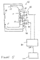
- FIGURE 1 shows an electrodeless lamp ballast circuit 10 incorporating a dimming system 12 , in an embodiment of the present invention.
- a d.c.-to-a.c. converter 13 of ballast 10 includes switches 14 and 16 which are respectively controlled to convert d.c. current from a source 18 , such as the output of a full-wave bridge (not shown) to a.c. current received by a load circuit 20 comprising a resonant inductor 22 and a resonant capacitor 24 .
- D.c. bus voltage, Vbus, 25 exists between bus conductor 26 and reference conductor 28.
- Load circuit 20 also includes electrodeless lamp 30 , and r.f. coil 32 which provides the energy to excite plasma of electrodeless lamp 30 to a state which generates light.
- a d.c. blocking capacitor 34 is connected between load circuit 20 and reference conductor 28 .
- Other arrangements for powering electrodeless lamp 30 by load circuit 20 and arrangements alternative to capacitor 34 are known in the art.
- switches 14 and 16 are complementary to each other in the sense, for instance, that switch 14 may be an n-channel enhancement mode device, and switch 16 a p-channel enhancement mode device.
- Each of switches 14 and 16 include an inherent, reverse-conducting diode (not shown).
- each switch 14 an d 16 has a respective gate, or control terminal, 36 and 38 .
- the voltage from gate 36 to a source 40 of switch 14 controls the conduction state of that switch.
- the voltage from gate 38 to a source 42 of switch 16 controls the conduction state of that switch.
- sources 40 and 42 are connected together at a common node 44 .
- control node 46 With gates 36 and 38 interconnected at a common control node 46 , the single voltage between control node 46 and common node 44 controls the conduction states of both switches 14 and 16 .
- the drains 48 and 50 of the switches are connected to bus conductor 26 and reference conductor 28 , respectively.
- Switches 14 and 16 could alternatively be embodied as Insulated Gate Bipolar Transistor (IGBT) switches, such as the p-channel and n-channel devices respectively. However, each IGBT switch would then be accompanied by a reverse-conducting diode (not shown).
- IGBTs Insulated Gate Bipolar Transistor
- MOSFETs MOSFETs
- switches 14 and 16 could be embodied as Bipolar Junction Transistor (BJT) switches, such as the NPN and PNP devices respectively. As with the IGBT switches, the BJT switches are respectively accompanied by reverse-conducting diodes (not shown).
- Gate drive circuit 52 connected between control node 46 and common node 44 , controls the conduction states of switches 14 and 16 .
- Gate drive circuit 52 includes a driving inductor 54 that is mutually coupled to resonant inductor 22 , and is connected at one end to common node 44.
- the end of inductor 22 connected to node 44 may be a tap from a transformer winding forming inductors 54 and 22 .
- Inductors 54 and 22 are poled in accordance with the solid dots shown adjacent the symbols for these inductors.
- Driving inductor 54 provides the driving energy for operation of gate drive circuit 52 .
- a second inductor 56 is serially connected to driving inductor 54 between node 46 and inductor 54 .
- Second inductor 56 is used to adjust the phase angle of the gate-to-source voltage appearing between nodes 46 and 44 .
- a bidirectional voltage clamp 58 between nodes 46 and 44 clamps positive and negative excursions of gate-to-source voltage to respective limits determined, e.g., by the voltage ratings of the back-to-back Zener diodes shown.
- a capacitor 60 is preferably provided between nodes 46 and 44 to predicably limit the rate of change of gate-to-source voltage between nodes 46 and 44 . This beneficially assures, for instance, a dead time interval in the switching modes of switches 14 and 16 wherein both switches are off between the times of either switch being turned on.
- a starting circuit includes a coupling capacitor 62 that becomes initially charged, upon energizing of source 18 , via resistors 64 , 66 and 68 .
- the voltage across capacitor 62 is zero, and, during the starting process, serial-connected inductors 54 and 56 act essentially as a short circuit, due to the relatively long time constant for charging of capacitor 62 .
- resistors 64-68 being of equal value, for instance, the voltage on nodes 44 and 46, upon initial bus energization, is approximately one-third of bus voltage 25 .
- capacitor 62 becomes increasingly charged, from left to right, until it reaches the threshold voltage of the gate-to-source voltage of upper switch 14 (e.g., 2-3 volts).
- upper switch 14 switches into its conduction mode, which then results in current being supplied by that switch to load circuit 20 .
- the resulting current in the load circuit causes regenerative control of first and second switches 14 and 16 .
- ballast circuit 10 During steady state operation of ballast circuit 10 , the voltage of common node 44 , between switches 14 and 16 , becomes approximately one-half of bus voltage 25 . With the voltage at node 46 , between resistors 64 and 66 also being approximately one-half bus voltage 25 for instance, capacitor 62 cannot again, during steady state operation, become charged through resistors 64 and 66 so as to again create a starting pulse for turning on switch 14 .
- the capacitive reactance of capacitor 62 is much smaller than the inductive reactance of driving inductor 54 and inductor 56 , so that capacitor 62 does not interfere with operation of those inductors.
- Resistor 68 may be alternatively placed to shunt upper switch 14 rather than lower switch 16 .
- the operation of the circuit is similar to that described above with respect to resistor 68 shunting lower switch 16 .
- node 44 assumes a higher potential than node 46 between resistors 64 and 66 , so tat capacitor 62 becomes charged from right to left. This results in an increasingly negative voltage between node 46 and node 44 , which is effective for turning on lower switch 16 .
- ballast circuit 10 does not require a triggering device, such as a diac, which is traditionally used for starting.
- resistors 64 , 66 and 68 are non-critical value components, which may be 100k ohms or 1 megohm each, for example. Preferably such resistors have similar values, e.g., approximately equal.
- oscillation signal 100 which is provided to r.f. coil 32 .
- oscillation signal 100 may operate at approximately 2.6 megahertz, which has approximately 400 nanosecond time periods.
- Dimming circuit 12 operates to controllably alter the frequency, and in particular, to raise the frequency of signal 100 of the circuit, to thereby move the load circuit out of resonance which in turn causes the voltage supplied to inductor 32 to drop. In this manner, voltage needed to induce the plasma of electrodeless lamp 30 is not available and the lamp enters a shutdown state.
- dimming circuit 12 uses a frequency shift keying (FSK) operation to achieve dimming of electrodeless lamp 30 , by shifting the frequency of ballast circuit 10 .
- Dimming circuit 12 includes dimming inductor 80 inductively coupled to inductor 56 of gate drive circuit 52.
- dimming circuit 12 can shunt the inductor voltage.
- Inductor 80 is coupled to a pair of dimming switches 82, 84 which are driven by a signal generator 86.
- dimming switches 82 and 84 may be two n-channel MOSFETS, where sources 92, 94 are tied together and drains 96, 98 are each connected to dimming inductor 80 .
- FIGURE 3 illustrates a FSK pulse signal which may be generated by signal generator 86 of FIGURE 1.
- signal generator 86 may be one of many known signal generators which can generate various waveforms of varying frequencies and with waveforms wit varying pulse widths.
- a pulse of FSK pulse signal 100 is applied to gates 88, 90 of transistors 82 and 84 , the frequency of ballast circuit 10 is shifted higher, causing the r.f. coil current to decrease, extinguishing the arc of electrodeless lamp 30 .
- a lower voltage is applied to r.f. coil 32, keeping the power dissipation in r.f. coil 32 and transistors 82 and 84 at safe levels.
- FIGURE 4 illustrates the frequency shift keying operation imposes the pulse wave form signal 102 of FIGURE 3 onto the carrier signal 100 of FIGURE 2. Specifically during a first time period 104 , the carrier signal is operating at the desired 2.6 megahertz value. However, once shutdown circuit 12 is activated, as shown during a second time period, 106 , the carrier frequency is increased to approximately 2.8 megahertz. This change in frequency causes a shutdown of the lamp to occur.
- a FSK cycle 108 is approximately 2 kHz, and therefore is approximately a one-half millisecond time period.
- the second time period 106 is approximately .5 millisecond. Therefore for the .5 millisecond time period the energy or power being put into lamp 30 is decreased.
- the amount of power being passed to lamp 30 is dictated by the width of the pulse supplied by pulse generator 86 .
- inductively coupled inductor 80 acts as a voltage source for dimming circuit 12 .
- Gate 88 of transistor 82 and gate 90 of transistor 84 are configured to receive the input pulse from signal source 86.
- Source 92 of transistor 82 and source 94 of transistor 84 are connected, and drain 96 of transistor 82 is connected to one end of inductor 80 while drain 98 of transistor 84 is connected to the opposite end of inductor 80 .
- Each of transistors 82, 84 has a diode 110, 112. These diodes are intrinsic to vertical transistors of the type being implemented in the present invention. It is to be appreciated that rather than imposing restrictions on the present invention, the intrinsic diodes are beneficially employed.
- signal source 86 applies a signal of sufficient value to the gates 88 and 90 , to exceed the threshold voltage of the gate source interface in order to turn on both transistors 82, 84 at the same time. By turning on transistors 82 and 84 current begins flowing in dimming circuit 12 .
- FIGURE 6 wherein current 114 is depicted in an equivalent resistive network.
- current 114 has a value of approximately 200 mA.
- transistor 82 its potential paths are either through channel 116 which has a resistance drain-to-source on (RDS-on) value of approximately 5 ohms, or through positive going diode 110 .
- RDS-on resistance drain-to-source on
- diode 110 Once transistor 82 has been turned on, the path with least resistance is diode 110 , and substantially all of current 114 will pass through diode 110 .
- diode 112 presents a substantially higher resistance than the RDS-on of transistor 84 , also approximately 5 ohms.
- the dimming circuit 12 essentially is a transistor in series with a diode rather than two transistors in the series due to the existence of the intrinsic diodes 110,112 . Under this arrangement, it is not necessary to use extremely low RDS-on devices as it is only necessary to ensure that the RDS-on of one transistor is sufficiently low, therefore in one embodiment transistors with RDS-on of up to 10 ohms or more may be used.
- the average power and therefore the average lumen output from lamp 30 can be controlled.
- Experimental data indicates that if the modulating wave form of FIGURE 3 is approximately 2 kHz, the light output can be varied from 20% to 100%. If the FSK period 108 is substantially outside the 2kHz range, desirable dimming does not occur as the signal does not allow lamp 30 to fully extinguish. On the other hand, if the modulating FSK wave form 102 is again substantially outside the 2kHz range, lamp 30 stays extinguished for too long a time period and undesirable voltage overshoots will occur at restarting of the lamp.
- the present invention may be used as a low-cost design for dimming the electrodeless lamp system.
- the input power to the system is less than 1.5 watts in a 23 watt system.
- transistors 82 and 84 are turned off, allowing the r.f. coil current to increase and restart the lamp, the power increases to approximately 100%, i.e. 23 watts.
- This dimming system may be used with lamp systems of various wattages, including but not being limited to 23 watts, 50 watts and 100 watts.
- the 2 kHz modulating wave form may be varied slightly to provide synchronization with the power line frequency if necessary.
- the ballast will have a line ripple due to filtering of input signals. Therefore it may be desirable, under certain circumstances, to provide a multiple of the ripple frequency so that the FSK modulating frequency is synchronized with the ripple. For example, it may be necessary to have the FSK modulating frequency at 10 - 15 times the ripple existing on the bus of the ballast.
- an operating set point to the dimming circuit 12, via a power line communication signal that can be supplied over a power line.
- signal generator 86 is provided with operating parameters from remote source 122 via communication lines 124 . Therefore the set point is provided remotely to the dimming circuitry.
- Another manner of transmitting a set point signal is to derive the set point from the power line and to provide a proportional signal to create pulse modulation used in the dimming circuit.
- Ballast circuit 10 operates at a frequency typically of about 2.5-2.6 Megahertz, which is about 10 to 20 times higher than for the electroded type of lamp powered by an appropriate ballast circuit.
- Exemplary component values for the circuit of Fig. 1 are as follows for a lamp 30 rated at 23 watts, with a d.c.
- switch 14 may be an IRFR210 or IRFR214, n-channel enhancement mode MOSFET, sold by International Rectifier Company, of El Segundo, California; and switch 16 , an IRFR9210 or IRFR9214, p-channel, enhancement mode MOSFET also sold by International Rectifier Company.
- Transistors 82 and 84 may be general application MOSFETS with 5-10 ohms, RDS-on and 50V maximum.
Landscapes
- Circuit Arrangements For Discharge Lamps (AREA)
- Discharge-Lamp Control Circuits And Pulse- Feed Circuits (AREA)
Abstract
Description
| | 20 micro |
| Driving inductor | |
| 54 | 0.2 micro henries |
| Turns ratio between 22 and 54 | 35:1 |
| | 1.5 |
| Capacitor | |
| 60 | 470 |
| Capacitor | |
| 62 | 22 |
| Zener diodes | |
| 58, each | 7.5 |
| Resistors | |
| 64, 66 and 68, each | 270k ohms |
| | 680 picofarads |
| D.c. blocking | 3.3 nanofarads |
| R.f. | 10 microhenries |
| Turns ratio between 56 and 80 | 1:1 |
wherein receipt of the modulated signal, initiates activation of the first and second dimming switches, and causes a current to flow through the first and second dimming switches, thereby decreasing the output of the d.c.-to-a.c. converter.
wherein receipt of the modulated signal initiates activation of the first and second dimming switches, and causes a current to flow through the first and second dimming switches, thereby decreasing the output of the d.c.-to-.a.c converter.
wherein when the switching network is activated, a current flows through the switching network, whereby a switching frequency of the ballast is increased, which lowers the voltage supplied to the r.f. inductor, whereby repeated activation and deactivation of the switching network generates an altering of the lumens output resulting in a perceived dimming the electrodeless lamp output.
Claims (10)
- In a ballast for an electrodeless lamp, a dimming circuit for decreasing output of a d.c.-to-a.c. converter for selective dimming of the electrodeless lamp, said dimming system comprising:a first dimming switch;a second dimming switch connected in series to the first dimming switch;a voltage source, a first-end of the voltage source connected to the first dimming switch and a second end of the voltage source connected to the second dimming switch;a signal source configured to generate a modulated signal, supplied to the first and second dimming switches,
wherein receipt of the modulated signal, initiates activation of the first and second dimming switches, and causes a current to flow through the first and second dimming switches, thereby decreasing the output of the d.c.-to-a.c. converter. - A circuit according to claim 1 wherein the ballast circuit further includes:a load circuit incorporating the electrodeless lamp and including a resonant inductance, a resonant capacitance, and a r.f. inductor;the d.c.-to-a.c. converter is coupled to said load circuit for inducing an a.c. current in said load circuit, said d.c.-to-a.c. converter comprising:(a) first and second switches serially connected between a bus conductor at a d.c. voltage and a reference conductor, and being connected together at a common node through which said a.c. load current flows;(b) a control node further connecting said first and second switches at a location other than the common node, wherein the voltage between the control node and the common node determines the conduction state of the switches; anda gate drive arrangement for regeneratively controlling said first and second switches; said arrangement comprising:(a) a driving inductor mutually coupled to said resonant inductor in such manner that a voltage is induced therein which is proportional to the instantaneous rate of change of said a.c. load current; said driving inductor being connected between said common node and said control node;(b) a second inductor serially connected to said driving inductor, with the serially connected driving inductor and second inductor being connected between said common node and said control node and said second inductor mutually coupled to said voltage source in such a manner that a voltage is induced therein; and(c) a bi-directional voltage clamp connected between said common node and said control node for limiting positive and negative excursions of voltage of said control node with respect to said common node.
- The circuit of claim 1 or 2 wherein the first dimming switch and the second dimming switch are MOSFETS.
- The circuit of claim 3 wherein the MOSFETS include intrinsic diodes.
- The circuit of any one of claims 1 to 4 wherein the voltage source is an inductor of the d.c.-to-a.c. converter inductively coupled to an inductor of the dimming circuit.
- A ballast circuit for an electrodeless lamp, comprising:a resonant load circuit incorporating the electrodeless lamp and including a resonant inductance, a resonant capacitance and a r.f. inductor;a d.c.-to-a.c. converter circuit coupled to said resonant load circuit for inducing an a.c. current in said resonant load circuit, said d.c.-to-a.c. converter circuit including an inductor across which is a voltage of the d.c.-to-a.c. converter;a drive arrangement for controlling operation of said d.c.-to-a.c. converter circuit; anda dimming circuit for limiting voltage output of the d.c.-to-a.c. converter circuit, said dimming circuit comprising:(a) a first dimming switch;(b) a second dimming switch connected in series to the first dimming switch;(c) a voltage source, a first end of the voltage source connected to the first dimming switch and a second end of the voltage source connected to the second dimming switch;(d) a signal source configured to generate a modulated signal, supplied to the first and second dimming switches,
wherein receipt of the modulated signal initiates activation of the first and second dimming switches, and causes a current to flow through the first and second dimming switches, thereby decreasing the output of the d.c.-to-.a.c converter. - A method of dimming an electrodeless fluorescent lamp energized by a ballast having a d.c.-to-a.c. converter which generates a voltage for an r.f. inductor for energizing the electrodeless fluorescent lamp, the dimming method comprising:generating a voltage source proportional to a voltage supplied to the r. f. inductor;supplying, from a signal source, a modulating signal to a switching network;turning on the switching network for a selected duty cycle when the modulating signal is supplied to the switching network,
wherein when the switching network is activated, a current flows through the switching network, whereby a switching frequency of the ballast is increased, which lowers the voltage supplied to the r.f. inductor, whereby repeated activation and deactivation of the switching network generates an altering of the lumens output resulting in a perceived dimming the electrodeless lamp output. - The circuit according to claim 7 wherein the duty cycles of the dimming network is adjustable so as to place the electrodeless lamp to an on state from 20% to 100% of a cycle of the modulating signal.
- The circuit according to claim 7 or 8 wherein the modulating signal is approximately 2kHz.
- The circuit according to claim 7, 8 or 9 wherein the modulating signal is controlled remotely of the ballast circuit.
Applications Claiming Priority (2)
| Application Number | Priority Date | Filing Date | Title |
|---|---|---|---|
| US09/318,343 US6175198B1 (en) | 1999-05-25 | 1999-05-25 | Electrodeless fluorescent lamp dimming system |
| US318343 | 2002-12-12 |
Publications (2)
| Publication Number | Publication Date |
|---|---|
| EP1056316A2 true EP1056316A2 (en) | 2000-11-29 |
| EP1056316A3 EP1056316A3 (en) | 2003-12-03 |
Family
ID=23237779
Family Applications (1)
| Application Number | Title | Priority Date | Filing Date |
|---|---|---|---|
| EP00304397A Withdrawn EP1056316A3 (en) | 1999-05-25 | 2000-05-24 | Electrodeless fluorescent lamp dimming system |
Country Status (4)
| Country | Link |
|---|---|
| US (1) | US6175198B1 (en) |
| EP (1) | EP1056316A3 (en) |
| JP (1) | JP2000353600A (en) |
| CN (1) | CN1290381C (en) |
Cited By (1)
| Publication number | Priority date | Publication date | Assignee | Title |
|---|---|---|---|---|
| WO2003032692A3 (en) * | 2001-10-08 | 2003-07-10 | Northrop Grumman Corp | Dimmable ballast for electrodeless fluorescent lamps |
Families Citing this family (18)
| Publication number | Priority date | Publication date | Assignee | Title |
|---|---|---|---|---|
| US6433492B1 (en) * | 2000-09-18 | 2002-08-13 | Northrop Grumman Corporation | Magnetically shielded electrodeless light source |
| US6392365B1 (en) | 2001-06-20 | 2002-05-21 | General Electric Company | Hot restrike protection circuit for self-oscillating lamp ballast |
| US6392366B1 (en) | 2001-09-19 | 2002-05-21 | General Electric Company | Traic dimmable electrodeless fluorescent lamp |
| US6756746B2 (en) * | 2001-09-19 | 2004-06-29 | General Electric Company | Method of delaying and sequencing the starting of inverters that ballast lamps |
| US6815908B2 (en) * | 2002-12-11 | 2004-11-09 | General Electric | Dimmable self-oscillating electronic ballast for fluorescent lamp |
| JP4433677B2 (en) * | 2003-02-14 | 2010-03-17 | パナソニック電工株式会社 | Electrodeless discharge lamp lighting device |
| CN2645232Y (en) * | 2003-08-04 | 2004-09-29 | 上海宏源照明电器有限公司 | Electromagnetic induction lamp with three-dimensional contouring tube |
| CN101273667B (en) | 2005-09-28 | 2010-12-29 | 松下电工株式会社 | Dimmable electronic ballasts and luminaires for electrodeless discharge lamps |
| JP4328336B2 (en) * | 2006-04-28 | 2009-09-09 | パナソニック電工株式会社 | Electrodeless discharge lamp device and lighting apparatus using the same |
| US7852471B2 (en) * | 2006-05-22 | 2010-12-14 | Varian Australia Pty Ltd | Power generator for spectrometry |
| JP4971739B2 (en) * | 2006-09-29 | 2012-07-11 | パナソニック株式会社 | Electrodeless discharge lamp lighting device and its lighting fixture |
| US7750577B2 (en) * | 2008-03-07 | 2010-07-06 | General Electric Company | Apparatus and method for providing an isolated set point from an input signal applied to a lamp ballast |
| US8581501B2 (en) | 2009-08-18 | 2013-11-12 | General Electric Company | Fluorescent dimming ballast with improved efficiency |
| US8274234B1 (en) | 2009-12-08 | 2012-09-25 | Universal Lighting Technologies, Inc. | Dimming ballast with parallel lamp operation |
| US8633653B2 (en) * | 2010-03-02 | 2014-01-21 | General Electric Company | Lighting control system with improved efficiency |
| CN201663749U (en) * | 2010-03-16 | 2010-12-01 | 陈敬昕 | Light-adjustable ballast device of electrodeless lamp |
| US8324813B1 (en) | 2010-07-30 | 2012-12-04 | Universal Lighting Technologies, Inc. | Electronic ballast with frequency independent filament voltage control |
| US9078307B2 (en) | 2012-12-21 | 2015-07-07 | General Electric Company | Fault protection system and method for fluorescent lamp ballasts |
Family Cites Families (19)
| Publication number | Priority date | Publication date | Assignee | Title |
|---|---|---|---|---|
| US4189661A (en) | 1978-11-13 | 1980-02-19 | Gte Laboratories Incorporated | Electrodeless fluorescent light source |
| US4249111A (en) | 1979-08-20 | 1981-02-03 | Pitney Bowes Inc. | Automatic lamp shutdown circuit |
| US4382212A (en) | 1981-02-09 | 1983-05-03 | Gte Products Corporation | One lamp out detect shutdown technique for high frequency, solid state fluorescent lamp ballasts |
| US4680508A (en) * | 1986-05-09 | 1987-07-14 | General Electric Company | Load control circuit |
| US5245253A (en) * | 1989-09-21 | 1993-09-14 | Etta Industries | Electronic dimming methods for solid state electronic ballasts |
| US5027041A (en) * | 1990-01-16 | 1991-06-25 | Gte Products Corporation | Integrated radio-frequency light source for large scale display |
| US5173643A (en) | 1990-06-25 | 1992-12-22 | Lutron Electronics Co., Inc. | Circuit for dimming compact fluorescent lamps |
| ATE134818T1 (en) * | 1990-10-10 | 1996-03-15 | Philips Electronics Nv | SWITCHING ARRANGEMENT |
| EP0566672A1 (en) | 1991-01-09 | 1993-10-27 | Welch Allyn, Inc. | Low wattage metal halide lamp apparatus |
| US5315214A (en) | 1992-06-10 | 1994-05-24 | Metcal, Inc. | Dimmable high power factor high-efficiency electronic ballast controller integrated circuit with automatic ambient over-temperature shutdown |
| US5561351A (en) | 1992-10-14 | 1996-10-01 | Diablo Research Corporation | Dimmer for electrodeless discharge lamp |
| US5373217A (en) | 1993-03-24 | 1994-12-13 | Osram Sylvania Inc. | Method and circuit for enhancing stability during dimming of electrodeless hid lamp |
| CA2145894A1 (en) | 1994-04-18 | 1995-10-19 | Louis R. Nerone | External metallization configuration for an electrodeless fluorescent lamp |
| US5850127A (en) | 1996-05-10 | 1998-12-15 | Philips Electronics North America Corporation | EBL having a feedback circuit and a method for ensuring low temperature lamp operation at low dimming levels |
| US5744912A (en) | 1996-06-26 | 1998-04-28 | So; Gin Pang | Electronic ballast having an oscillator shutdown circuit for single or multiple fluorescent tubes for lamps |
| US5877595A (en) | 1996-09-06 | 1999-03-02 | General Electric Company | High power factor ballast circuit with complementary converter switches |
| US5965985A (en) * | 1996-09-06 | 1999-10-12 | General Electric Company | Dimmable ballast with complementary converter switches |
| US5796214A (en) | 1996-09-06 | 1998-08-18 | General Elecric Company | Ballast circuit for gas discharge lamp |
| US5874810A (en) | 1997-09-02 | 1999-02-23 | General Electric Company | Electrodeless lamp arrangement wherein the excitation coil also forms the primary of the feedback transformer used to switch the transistors of the arrangement |
-
1999
- 1999-05-25 US US09/318,343 patent/US6175198B1/en not_active Expired - Lifetime
-
2000
- 2000-05-23 JP JP2000150707A patent/JP2000353600A/en active Pending
- 2000-05-24 EP EP00304397A patent/EP1056316A3/en not_active Withdrawn
- 2000-05-25 CN CNB001089897A patent/CN1290381C/en not_active Expired - Fee Related
Cited By (1)
| Publication number | Priority date | Publication date | Assignee | Title |
|---|---|---|---|---|
| WO2003032692A3 (en) * | 2001-10-08 | 2003-07-10 | Northrop Grumman Corp | Dimmable ballast for electrodeless fluorescent lamps |
Also Published As
| Publication number | Publication date |
|---|---|
| US6175198B1 (en) | 2001-01-16 |
| CN1293531A (en) | 2001-05-02 |
| JP2000353600A (en) | 2000-12-19 |
| CN1290381C (en) | 2006-12-13 |
| EP1056316A3 (en) | 2003-12-03 |
Similar Documents
| Publication | Publication Date | Title |
|---|---|---|
| US6175198B1 (en) | Electrodeless fluorescent lamp dimming system | |
| US4998046A (en) | Synchronized lamp ballast with dimming | |
| US6570343B1 (en) | Device for turning on light and illumination apparatus | |
| US6392366B1 (en) | Traic dimmable electrodeless fluorescent lamp | |
| US6218788B1 (en) | Floating IC driven dimming ballast | |
| US6339298B1 (en) | Dimming ballast resonant feedback circuit | |
| US6023132A (en) | Electronic ballast deriving auxilliary power from lamp output | |
| EP1987705B1 (en) | Voltage fed inverter for fluorescent lamps | |
| US6570347B2 (en) | Gas-discharge lamp having brightness control | |
| CN101326861B (en) | Apparatus and method for controlling filament voltage in an electronic dimming ballast | |
| US20090200965A1 (en) | Energy savings circuitry for a lighting ballast | |
| US20090200953A1 (en) | Methods and apparatus for a high power factor ballast having high efficiency during normal operation and during dimming | |
| US5055742A (en) | Gas discharge lamp dimming system | |
| US20090058302A1 (en) | Thermal foldback for linear fluorescent lamp ballasts | |
| US5089925A (en) | Protection device for electronic circuit | |
| EP1157591A1 (en) | Hid ballast with hot restart circuit | |
| WO2000022889A2 (en) | Hid ballast circuit with arc stabilization | |
| JPH076621A (en) | Device for modulating light of discharge lamp | |
| US6208086B1 (en) | Halogen power converter with complementary switches | |
| EP1521508A1 (en) | Method and apparatus for a unidirectional switching, current limited cutoff circuit for an electronic ballast | |
| JP2004521467A (en) | Circuit device | |
| GB2226463A (en) | Control of fluorescent lights | |
| JP2868240B2 (en) | Discharge lamp lighting device | |
| WO2003101159A1 (en) | Lamp ballast with series switchable inductor | |
| KR860001277B1 (en) | Adjustable electrical power control for gas discharge lamps and the like |
Legal Events
| Date | Code | Title | Description |
|---|---|---|---|
| PUAI | Public reference made under article 153(3) epc to a published international application that has entered the european phase |
Free format text: ORIGINAL CODE: 0009012 |
|
| AK | Designated contracting states |
Kind code of ref document: A2 Designated state(s): AT BE CH CY DE DK ES FI FR GB GR IE IT LI LU MC NL PT SE |
|
| AX | Request for extension of the european patent |
Free format text: AL;LT;LV;MK;RO;SI |
|
| PUAL | Search report despatched |
Free format text: ORIGINAL CODE: 0009013 |
|
| AK | Designated contracting states |
Kind code of ref document: A3 Designated state(s): AT BE CH CY DE DK ES FI FR GB GR IE IT LI LU MC NL PT SE |
|
| AX | Request for extension of the european patent |
Extension state: AL LT LV MK RO SI |
|
| RIC1 | Information provided on ipc code assigned before grant |
Ipc: 7H 05B 41/28 B Ipc: 7H 05B 41/392 A |
|
| 17P | Request for examination filed |
Effective date: 20040603 |
|
| AKX | Designation fees paid |
Designated state(s): DE FR GB IT |
|
| 17Q | First examination report despatched |
Effective date: 20060629 |
|
| GRAP | Despatch of communication of intention to grant a patent |
Free format text: ORIGINAL CODE: EPIDOSNIGR1 |
|
| STAA | Information on the status of an ep patent application or granted ep patent |
Free format text: STATUS: THE APPLICATION IS DEEMED TO BE WITHDRAWN |
|
| 18D | Application deemed to be withdrawn |
Effective date: 20090509 |