EP1056195A2 - A multiple differential pair transistor architecture having transconductance proportional to bias current for any transitor technology - Google Patents
A multiple differential pair transistor architecture having transconductance proportional to bias current for any transitor technology Download PDFInfo
- Publication number
- EP1056195A2 EP1056195A2 EP00304051A EP00304051A EP1056195A2 EP 1056195 A2 EP1056195 A2 EP 1056195A2 EP 00304051 A EP00304051 A EP 00304051A EP 00304051 A EP00304051 A EP 00304051A EP 1056195 A2 EP1056195 A2 EP 1056195A2
- Authority
- EP
- European Patent Office
- Prior art keywords
- differential
- transconductance
- circuit
- current
- transistors
- Prior art date
- Legal status (The legal status is an assumption and is not a legal conclusion. Google has not performed a legal analysis and makes no representation as to the accuracy of the status listed.)
- Granted
Links
Images


Classifications
-
- H—ELECTRICITY
- H03—ELECTRONIC CIRCUITRY
- H03F—AMPLIFIERS
- H03F3/00—Amplifiers with only discharge tubes or only semiconductor devices as amplifying elements
- H03F3/45—Differential amplifiers
- H03F3/45071—Differential amplifiers with semiconductor devices only
- H03F3/45076—Differential amplifiers with semiconductor devices only characterised by the way of implementation of the active amplifying circuit in the differential amplifier
- H03F3/45179—Differential amplifiers with semiconductor devices only characterised by the way of implementation of the active amplifying circuit in the differential amplifier using MOSFET transistors as the active amplifying circuit
- H03F3/45183—Long tailed pairs
-
- H—ELECTRICITY
- H03—ELECTRONIC CIRCUITRY
- H03F—AMPLIFIERS
- H03F3/00—Amplifiers with only discharge tubes or only semiconductor devices as amplifying elements
- H03F3/45—Differential amplifiers
- H03F3/45071—Differential amplifiers with semiconductor devices only
- H03F3/45076—Differential amplifiers with semiconductor devices only characterised by the way of implementation of the active amplifying circuit in the differential amplifier
- H03F3/4508—Differential amplifiers with semiconductor devices only characterised by the way of implementation of the active amplifying circuit in the differential amplifier using bipolar transistors as the active amplifying circuit
- H03F3/45085—Long tailed pairs
-
- H—ELECTRICITY
- H03—ELECTRONIC CIRCUITRY
- H03F—AMPLIFIERS
- H03F1/00—Details of amplifiers with only discharge tubes, only semiconductor devices or only unspecified devices as amplifying elements
- H03F1/32—Modifications of amplifiers to reduce non-linear distortion
- H03F1/3211—Modifications of amplifiers to reduce non-linear distortion in differential amplifiers
Definitions
- the present invention relates to multiple differential transistor pair circuits, and more particularly, to linear multiple differential transistor pair circuits.
- Multiple differential pair circuits consist of N differential pairs of transistors operating in parallel, each having an appropriate input offset voltage.
- Multiple differential pair circuits are well-known and have many applications, including amplifiers, mixers, filters and other active elements.
- amplifiers, mixers, filters and other active elements For a detailed discussion of conventional multiple differential pair circuits implemented in bipolar technology and their applications, see, for example, B. Gilbert, “The Multi-Tanh Principle: A tutorial Overview," IEEE J. of Solid-State Circuits, Vol. 33, 2-17 (Jan. 1998), incorporated by reference herein.
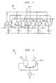
- FIG. 1 illustrates a conventional multiple differential pair circuit 100.
- the illustrative multiple differential pair circuit 100 consists of five (5) differential pairs of transistors 200-1 through 200-5 coupled in parallel.
- a representative differential transistor pair circuit 200 is discussed below in conjunction with FIG. 2.
- the differential transistor pair circuit 200-3 in the middle of the multiple differential pair circuit 100 does not have an offset voltage, while the other differential transistor pair circuits 200-1, 200-2, 200-4, 200-5 have a corresponding offset, ⁇ .
- the offset voltage, ⁇ increases progressively, taking values of ⁇ , ⁇ 2 ⁇ and so on, in a known manner.
- such circuits are referred to as equidistant-offset multiple differential pair circuits.
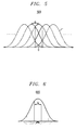
- FIG. 2 is a schematic block diagram of a representative differential transistor pair circuit 200.
- the two transistor devices 210-1 and 210-2 that comprise the differential transistor pair circuit 200 are identical (i.e., perfectly matched), in a known manner.
- a desired output current, I 1 , I 2 can be obtained from the differential transistor pair circuit 200 by varying the bias current, I O .
- Bipolar transistors and thus, bipolar differential transistor pair circuits 200, have well-defined voltage-current (V-I) characteristics.
- Differential transistor pair circuits 200 have been implemented using bipolar transistors (or CMOS transistors operating in sub-threshold ranges where they behave like bipolar transistors), where the voltage-current (V-I) characteristic is exponential.
- FIG. 3 illustrates the voltage-current (V-I) characteristic 300 of the differential transistor pair circuit 200, shown in FIG. 2.
- Transistors having exponential voltage-current (V-I) characteristics were thought to be required in order to obtain multiple differential pair circuits 100 having a transconductance, g m , that is linearly proportional to the bias current.
- V-I voltage-current
- a multiple differential pair circuit having a transconductance, g m , proportional to the bias current, I 0 , for any transistor technology.
- the transistors utilized to construct each of the differential transistor pairs in a multiple differential pair circuit are permitted to have a non-exponential voltage-current (V-I) characteristic.
- the transistors are embodied as MOS transistors. The present invention thus allows multiple differential pair circuits with transconductance, g m , proportional to bias current to be fabricated in any transistor technology.
- the effective transconductance, g m becomes (i) linearly dependent on bias current, and (ii) insensitive to the voltage-current (V-I) characteristics of the utilized devices.
- V-I voltage-current
- Methods and apparatus are disclosed that provide a linear transconductance, g m , with respect to the bias current, I 0 , using differential pairs of transistors where each transistor has a non-exponential voltage-current (V-I) characteristic.
- the multiple differential pair circuits of the present invention may be constructed in the same manner as the conventional multiple differential pair circuit 100 shown in FIG. 1, as modified herein to provide the features and functions of the present invention.
- the transistors 210-1, 210-2 in each of the differential transistor pair circuits 200-N have a non-exponential voltage-current (V-I) characteristic, such as MOS transistors. In this manner, the multiple differential pair circuits 100 of the present invention can be fabricated without regard to the transistor technology.
- V-I voltage-current
- transconductance characteristic, g m , 400 of the differential transistor pair circuit 200 is shown in FIG. 4.
- the transconductance, g m is the ratio of the incremental change in the output current, I 1 , I 2 , of the differential transistor pair circuit 200 to the incremental change in the input voltage, V IN , when the bias current, I 0 , is kept constant.
- the transconductance characteristic, g m , 400 is a symmetric function of V in .
- the shape of the transconductance characteristic, g m , 400 strongly depends on the voltage-current (V-I) characteristic of the transistors 210-1, 210-2 in each differential transistor pair circuit 200.
- the present invention recognizes, however, that the area under the transconductance characteristic, g m , 400 is completely independent of the device characteristics.
- the area under the transconductance characteristic, g m , 400 equals the absolute change of the output current, I 1 , I 2 .
- the absolute change of the output current, I 1 , I 2 is equal to the bias or tail current, I 0 .
- the following expression holds:
- the symmetry of the transconductance characteristic, g m , 400 and the constancy of the area under the transconductance characteristic, g m , 400 are the two properties exploited by the present invention.
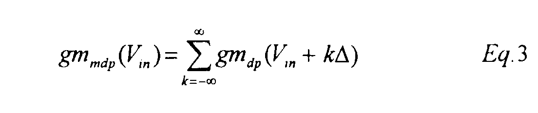
- FIG. 5 illustrates the transconductance, gm mdp , of a multiple differential pair circuit 100 as a sum of identical ⁇ -spaced gm dp functions.
- the transconductance function, g m of such a circuit is the sum of the infinitely many identical ⁇ -spaced gm dp functions.
- the transconductance, g m is clearly an even periodic function of V in (with a period of ⁇ ).
- the transconductance, g m can be written in the form: where all ak coefficients have dimensions A/V and Thus, a 0 determines the average value of gm mdp , while all higher-order coefficients (a k , k ⁇ 1) determine its ripple.
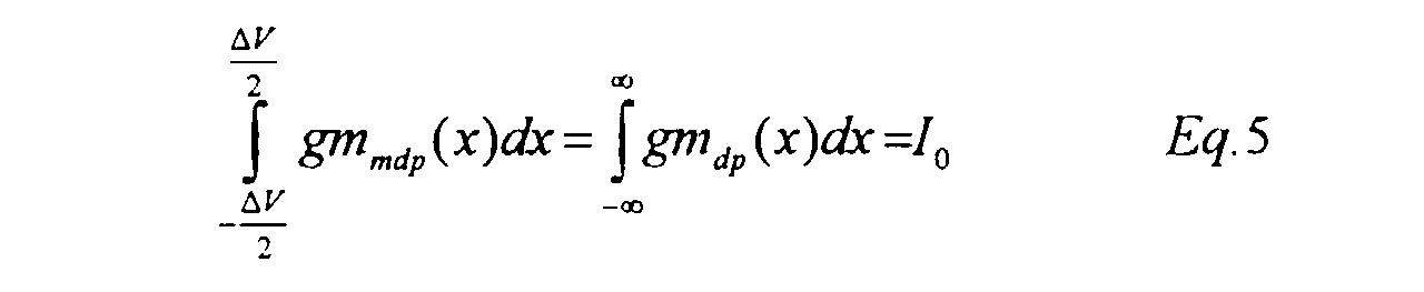
- FIG. 6 illustrates the transconductance, gm mdp , of a multiple differential pair circuit 100 in a ⁇ region as a "sliced and overlaid" gm dp function.
- the gm mdp in the region ⁇ ⁇ / 2 can be viewed as a result of slicing a single gm dp function into ⁇ -pieces and overlaying them on top of each other.
- the area under the gm mdp in the region ⁇ ⁇ / 2 equals the total area under a single gm dp curve.
- a 0 depends only on the biasing (I 0 and ⁇ ) and not on the voltage-current (V-I) characteristic of the utilized transistors. High linearity (small R(V in )) can be achieved by proper selection of the offset voltage, ⁇ .
- Equation 7 shows that as a multiple differential pair circuit 100 is being linearized, the effective transconductance, g m , becomes (i) linearly dependent on bias current, and (ii) insensitive to the voltage-current (V-I) characteristics of the utilized devices 210.
- the transconductance, g m can be made nearly temperature, supply and process independent by making I 0 and ⁇ temperature, supply and process independent. This task can be accomplished in any technology using well-known band-gap-based bias techniques.
- the transconductance, g m of a multiple differential pair circuit 100 employing a finite number of differential transistor pair circuits 200 has three different regions, namely, a middle region and two end regions.
- the middle region is the range of input voltages V in for which the following holds: Therefore, in the middle region, the operation and the properties of the finite-pair circuit 100 are identical to those of the infinite-pair circuit 100, discussed above.
- the middle region may or may not exist.
- the effect of having a finite number of transistor pairs 200 in the multiple differential pair circuit 100 is observed in the end regions.
- gm mdp has a value that is smaller than the nominal (and desired) I 0 / ⁇ .
- the end regions of a bipolar circuit do not change with I 0 while those of MOS circuits grow with I 0 .
- This difference is the direct consequence of the fact that the spread of gm dp of a bipolar differential transistor pair circuit 200 does not change with I 0 while the spread of the gm dp of a MOS differential transistor pair circuit 200 increases with I 0 2 .
- FIG. 7 illustrates the transconductance characteristic, g m , 700 of an equidistant-offset multiple differential pair circuit implemented in MOS technology.
- the increase of the end regions, such as the end regions 710, 730, in MOS multiple differential pair circuits 100 causes a decrease of the available mid-region 720.
- multiple differential pair circuit 100 implemented in MOS technology can provide reasonable input linear range and a decade of linear-with-current tuning.
Landscapes
- Engineering & Computer Science (AREA)
- Power Engineering (AREA)
- Physics & Mathematics (AREA)
- Nonlinear Science (AREA)
- Amplifiers (AREA)
- Networks Using Active Elements (AREA)
Abstract
Description





Claims (14)
- A multiple differential pair circuit having a transconductance, gm, that varies linearly with a bias current, I0, said circuit comprising a plurality of differential transistor pair circuits coupled in parallel, wherein said differential transistor pair circuits are comprised of transistors having a non-exponential voltage-current (V-I) characteristic.
- The multiple differential pair circuit of claim 1, wherein said transistors are MOS transistors.
- The multiple differential pair circuit of claim 1, wherein the control terminals of each of said differential transistor pair circuits are coupled.
- The multiple differential pair circuit of claim 1, wherein the output terminals of each of said differential transistor pair circuits are coupled.
- The multiple differential pair circuit of claim 1, wherein the transconductance, gm, is constant as an applied voltage, Vin, is varied.
- The multiple differential pair circuit of claim 1, wherein the transconductance, gm, varies linearly as said bias current, I0, is varied.
- A method of linearly varying the transconductance, gm, of a multiple differential pair circuit with respect to an bias current, I0, said method comprising the steps of:coupling a plurality of differential transistor pair circuits in parallel, wherein said differential transistor pair circuits are comprised of transistors having a non-exponential voltage-current (V-I) characteristic; andvarying the transconductance, gm, of said multiple differential pair circuit by applying said bias current, I0, to each of said differential pairs.
- The method of claim 5, wherein said transistors are MOS transistors.
- The method of claim 5, further comprising the step of coupling the control terminals of each of said differential transistor pair circuits.
- The method of claim 5, further comprising the step of coupling the output terminals of each of said differential transistor pair circuits.
- A multiple differential pair circuit having a transconductance, gm, that varies linearly with a bias current, I0, comprising:a plurality of differential transistor pair circuits coupled in parallel, wherein said differential transistor pair circuits are comprised of transistors having a non-exponential voltage-current (V-I) characteristic;at least one voltage source for applying an offset voltage, A, to each of said differential pairs; andat least one current source for applying said bias current, I0, to each of said differential pairs.
- A gain control circuit comprised of:
at least one multiple differential pair circuit having a transconductance, gm, that varies linearly with a bias current, I0, said circuit comprising a plurality of differential transistor pair circuits coupled in parallel, wherein said differential transistor pair circuits are comprised of transistors having a non-exponential voltage-current (V-I) characteristic. - An analog multiplier comprised of:
at least one multiple differential pair circuit having a transconductance, gm, that varies linearly with a bias current, I0, said circuit comprising a plurality of differential transistor pair circuits coupled in parallel, wherein said differential transistor pair circuits are comprised of transistors having a non-exponential voltage-current (V-I) characteristic. - A filter comprised of:
at least one multiple differential pair circuit having a transconductance, gm, that varies linearly with a bias current, I0, said circuit comprising a plurality of differential transistor pair circuits coupled in parallel, wherein said differential transistor pair circuits are comprised of transistors having a non-exponential voltage-current (V-I) characteristic.
Applications Claiming Priority (2)
| Application Number | Priority Date | Filing Date | Title |
|---|---|---|---|
| US322961 | 1989-03-14 | ||
| US09/322,961 US6211717B1 (en) | 1999-05-28 | 1999-05-28 | Multiple differential pair transistor architecture having transconductance proportional to bias current for any transistor technology |
Publications (3)
| Publication Number | Publication Date |
|---|---|
| EP1056195A2 true EP1056195A2 (en) | 2000-11-29 |
| EP1056195A3 EP1056195A3 (en) | 2004-07-28 |
| EP1056195B1 EP1056195B1 (en) | 2010-09-15 |
Family
ID=23257205
Family Applications (1)
| Application Number | Title | Priority Date | Filing Date |
|---|---|---|---|
| EP00304051A Expired - Lifetime EP1056195B1 (en) | 1999-05-28 | 2000-05-15 | A multiple differential pair transistor architecture having transconductance proportional to bias current for any transitor technology |
Country Status (5)
| Country | Link |
|---|---|
| US (1) | US6211717B1 (en) |
| EP (1) | EP1056195B1 (en) |
| JP (1) | JP3664946B2 (en) |
| KR (1) | KR20010029754A (en) |
| DE (1) | DE60044961D1 (en) |
Families Citing this family (6)
| Publication number | Priority date | Publication date | Assignee | Title |
|---|---|---|---|---|
| KR20050026668A (en) | 2003-09-09 | 2005-03-15 | 한국전자통신연구원 | Method for acquiring the high linearity and low distortion characteristic in triode-typed transconductor and triode-typed transconductor circuit applying the same |
| US7960436B2 (en) * | 2006-06-05 | 2011-06-14 | Valeant Pharmaceuticals International | Substituted arylamino-1,2,3,4-tetrahydro naphthalenes and-2,3-dihydro-1H-indenes as potassium channel modulators |
| KR100768091B1 (en) | 2006-08-25 | 2007-10-17 | 한국전자통신연구원 | Triode region transconductor circuit with wide linear range |
| US9018713B2 (en) | 2012-06-25 | 2015-04-28 | International Business Machines Corporation | Plural differential pair employing FinFET structure |
| US9024387B2 (en) | 2012-06-25 | 2015-05-05 | International Business Machines Corporation | FinFET with body contact |
| RU199328U1 (en) * | 2020-03-11 | 2020-08-28 | Максим Игоревич Кузьменко | Composite transistor |
Family Cites Families (3)
| Publication number | Priority date | Publication date | Assignee | Title |
|---|---|---|---|---|
| JP2687713B2 (en) * | 1990-10-30 | 1997-12-08 | 日本電気株式会社 | Logarithmic amplifier circuit |
| JPH088457B2 (en) * | 1992-12-08 | 1996-01-29 | 日本電気株式会社 | Differential amplifier circuit |
| US5602504A (en) * | 1995-09-15 | 1997-02-11 | National Science Council | Four-quadrant three-input multiplier |
-
1999
- 1999-05-28 US US09/322,961 patent/US6211717B1/en not_active Expired - Lifetime
-
2000
- 2000-05-15 DE DE60044961T patent/DE60044961D1/en not_active Expired - Lifetime
- 2000-05-15 EP EP00304051A patent/EP1056195B1/en not_active Expired - Lifetime
- 2000-05-24 JP JP2000153337A patent/JP3664946B2/en not_active Expired - Fee Related
- 2000-05-27 KR KR1020000028842A patent/KR20010029754A/en not_active Ceased
Also Published As
| Publication number | Publication date |
|---|---|
| JP3664946B2 (en) | 2005-06-29 |
| KR20010029754A (en) | 2001-04-16 |
| EP1056195A3 (en) | 2004-07-28 |
| JP2001024452A (en) | 2001-01-26 |
| US6211717B1 (en) | 2001-04-03 |
| EP1056195B1 (en) | 2010-09-15 |
| DE60044961D1 (en) | 2010-10-28 |
Similar Documents
| Publication | Publication Date | Title |
|---|---|---|
| US6304128B1 (en) | Continuous time capacitor-tuner integrator | |
| US7301391B2 (en) | Filtering variable offset amplifier | |
| US4723110A (en) | Transconductance amplifier | |
| JP3361021B2 (en) | Filter circuit | |
| EP1614218B1 (en) | Linear amplifier | |
| US20130162338A1 (en) | Tunable transconductance-capacitance filter with coefficients independent of variations in process corner, temperature, and input supply voltage | |
| JP3115741B2 (en) | Transconductance cell with improved linearity | |
| EP0438911A1 (en) | Integrated filter circuit | |
| EP1056195B1 (en) | A multiple differential pair transistor architecture having transconductance proportional to bias current for any transitor technology | |
| US6466090B1 (en) | Digitally programmable continuous-time modules for signal processing | |
| EP0052117B1 (en) | Current mode biquadratic active filter | |
| US10541675B1 (en) | Multi-gain transconductance amplifier | |
| EP0655831B1 (en) | High performance transconductance operational amplifier, of the CMOS integrated type | |
| US6545502B1 (en) | High frequency MOS fixed and variable gain amplifiers | |
| US6433626B1 (en) | Current-mode filter with complex zeros | |
| JP2783776B2 (en) | Operational transconductance amplifier | |
| US10382011B2 (en) | Grounded capacitance multipliers with electronic tuning possibility using single current feedback amplifier | |
| GB2295289A (en) | Wideband constant impedance amplifiers | |
| JPH11506580A (en) | Intermediate frequency amplifier / limiter | |
| Chaichana et al. | Current-mode MISO filter using CCCDTAs and grounded capacitors | |
| US20060214726A1 (en) | Q value correction of filter circuit | |
| JPH10126179A (en) | Gain control circuit and method | |
| US5177382A (en) | Active filter circuit | |
| US6570427B2 (en) | Variable transconductance amplifier | |
| EP1271777B1 (en) | A digital technologic attenuate control circuit of current-model step by step |
Legal Events
| Date | Code | Title | Description |
|---|---|---|---|
| PUAI | Public reference made under article 153(3) epc to a published international application that has entered the european phase |
Free format text: ORIGINAL CODE: 0009012 |
|
| AK | Designated contracting states |
Kind code of ref document: A2 Designated state(s): AT BE CH CY DE DK ES FI FR GB GR IE IT LI LU MC NL PT SE |
|
| AX | Request for extension of the european patent |
Free format text: AL;LT;LV;MK;RO;SI |
|
| PUAL | Search report despatched |
Free format text: ORIGINAL CODE: 0009013 |
|
| AK | Designated contracting states |
Kind code of ref document: A3 Designated state(s): AT BE CH CY DE DK ES FI FR GB GR IE IT LI LU MC NL PT SE |
|
| AX | Request for extension of the european patent |
Extension state: AL LT LV MK RO SI |
|
| 17P | Request for examination filed |
Effective date: 20050126 |
|
| AKX | Designation fees paid |
Designated state(s): DE FR GB |
|
| RAP3 | Party data changed (applicant data changed or rights of an application transferred) |
Owner name: LUCENT TECHNOLOGIES INC. |
|
| GRAP | Despatch of communication of intention to grant a patent |
Free format text: ORIGINAL CODE: EPIDOSNIGR1 |
|
| GRAS | Grant fee paid |
Free format text: ORIGINAL CODE: EPIDOSNIGR3 |
|
| GRAA | (expected) grant |
Free format text: ORIGINAL CODE: 0009210 |
|
| AK | Designated contracting states |
Kind code of ref document: B1 Designated state(s): DE FR GB |
|
| REG | Reference to a national code |
Ref country code: GB Ref legal event code: FG4D |
|
| REF | Corresponds to: |
Ref document number: 60044961 Country of ref document: DE Date of ref document: 20101028 Kind code of ref document: P |
|
| PLBE | No opposition filed within time limit |
Free format text: ORIGINAL CODE: 0009261 |
|
| STAA | Information on the status of an ep patent application or granted ep patent |
Free format text: STATUS: NO OPPOSITION FILED WITHIN TIME LIMIT |
|
| 26N | No opposition filed |
Effective date: 20110616 |
|
| REG | Reference to a national code |
Ref country code: DE Ref legal event code: R097 Ref document number: 60044961 Country of ref document: DE Effective date: 20110616 |
|
| PGFP | Annual fee paid to national office [announced via postgrant information from national office to epo] |
Ref country code: FR Payment date: 20140509 Year of fee payment: 15 |
|
| PGFP | Annual fee paid to national office [announced via postgrant information from national office to epo] |
Ref country code: GB Payment date: 20150424 Year of fee payment: 16 |
|
| REG | Reference to a national code |
Ref country code: FR Ref legal event code: ST Effective date: 20160129 |
|
| PG25 | Lapsed in a contracting state [announced via postgrant information from national office to epo] |
Ref country code: FR Free format text: LAPSE BECAUSE OF NON-PAYMENT OF DUE FEES Effective date: 20150601 |
|
| GBPC | Gb: european patent ceased through non-payment of renewal fee |
Effective date: 20160515 |
|
| PG25 | Lapsed in a contracting state [announced via postgrant information from national office to epo] |
Ref country code: GB Free format text: LAPSE BECAUSE OF NON-PAYMENT OF DUE FEES Effective date: 20160515 |
|
| REG | Reference to a national code |
Ref country code: DE Ref legal event code: R082 Ref document number: 60044961 Country of ref document: DE Representative=s name: DILG HAEUSLER SCHINDELMANN PATENTANWALTSGESELL, DE Ref country code: DE Ref legal event code: R081 Ref document number: 60044961 Country of ref document: DE Owner name: AVAGO TECHNOLOGIES GENERAL IP (SINGAPORE) PTE., SG Free format text: FORMER OWNER: LUCENT TECHNOLOGIES INC., MURRAY HILL, N.J., US Ref country code: DE Ref legal event code: R081 Ref document number: 60044961 Country of ref document: DE Owner name: AVAGO TECHNOLOGIES INTERNATIONAL SALES PTE. LI, SG Free format text: FORMER OWNER: LUCENT TECHNOLOGIES INC., MURRAY HILL, N.J., US |
|
| REG | Reference to a national code |
Ref country code: DE Ref legal event code: R081 Ref document number: 60044961 Country of ref document: DE Owner name: AVAGO TECHNOLOGIES INTERNATIONAL SALES PTE. LI, SG Free format text: FORMER OWNER: AVAGO TECHNOLOGIES GENERAL IP (SINGAPORE) PTE. LTD., SINGAPORE, SG Ref country code: DE Ref legal event code: R082 Ref document number: 60044961 Country of ref document: DE Representative=s name: DILG HAEUSLER SCHINDELMANN PATENTANWALTSGESELL, DE |
|
| PGFP | Annual fee paid to national office [announced via postgrant information from national office to epo] |
Ref country code: DE Payment date: 20190530 Year of fee payment: 20 |
|
| REG | Reference to a national code |
Ref country code: DE Ref legal event code: R071 Ref document number: 60044961 Country of ref document: DE |