EP1055178B1 - Data processor integrated circuit with a memory interface unit with programmable strobes to select different memory devices - Google Patents
Data processor integrated circuit with a memory interface unit with programmable strobes to select different memory devices Download PDFInfo
- Publication number
- EP1055178B1 EP1055178B1 EP99964480A EP99964480A EP1055178B1 EP 1055178 B1 EP1055178 B1 EP 1055178B1 EP 99964480 A EP99964480 A EP 99964480A EP 99964480 A EP99964480 A EP 99964480A EP 1055178 B1 EP1055178 B1 EP 1055178B1
- Authority
- EP
- European Patent Office
- Prior art keywords
- memory
- bank
- memory bank
- strobe
- address
- Prior art date
- Legal status (The legal status is an assumption and is not a legal conclusion. Google has not performed a legal analysis and makes no representation as to the accuracy of the status listed.)
- Expired - Lifetime
Links
Images



Classifications
-
- G—PHYSICS
- G06—COMPUTING OR CALCULATING; COUNTING
- G06F—ELECTRIC DIGITAL DATA PROCESSING
- G06F13/00—Interconnection of, or transfer of information or other signals between, memories, input/output devices or central processing units
- G06F13/14—Handling requests for interconnection or transfer
- G06F13/16—Handling requests for interconnection or transfer for access to memory bus
-
- G—PHYSICS
- G11—INFORMATION STORAGE
- G11C—STATIC STORES
- G11C8/00—Arrangements for selecting an address in a digital store
- G11C8/12—Group selection circuits, e.g. for memory block selection, chip selection, array selection
-
- G—PHYSICS
- G06—COMPUTING OR CALCULATING; COUNTING
- G06F—ELECTRIC DIGITAL DATA PROCESSING
- G06F13/00—Interconnection of, or transfer of information or other signals between, memories, input/output devices or central processing units
- G06F13/14—Handling requests for interconnection or transfer
- G06F13/16—Handling requests for interconnection or transfer for access to memory bus
- G06F13/1668—Details of memory controller
- G06F13/1694—Configuration of memory controller to different memory types
Definitions
- the present invention relates to a data processor integrated circuit with a memory interface unit for coupling a microprocessor to a memory external to the microprocessor, and to input/output devices of a memory-mapped type.
- a programmable memory interface for efficient transfer of different size data between a microprocessor of a given data and address bus width and memory banks of various data and address width, typically differing from the widths of the microprocessor's buses.
- the microprocessor which has a 32 bit internal architecture, can execute programming code from 16 or 32 bit wide external memories, and can load and store 8, 16, and 32 bit data units into external memory and convert them into an internally equivalent 32 bit representation.
- one external pin configures the memory width to 16 or 32 bit, and two sets of memory strobes and one I/O (input/output) strobe allow zero glue logic to two banks of memory and one bank of external peripherals.
- memory strobes and one I/O (input/output) strobe allow zero glue logic to two banks of memory and one bank of external peripherals.
- one or two of four pins, otherwise all used as strobe-byte enable pins, are used as additional address pins. The behavior of the pins is manipulated according to the contents of certain registers. All memory banks are of the same directly addressable type.
- a microcomputer with a programmable multifunction port is disclosed.
- One of a plurality of ports is user programmable by application of specific signals to mode selection pins.
- the programmable port comprises a number of lines which can be programmed as input or output lines to peripheral equipment, or, alternatively, can be programmed to serve as a bi-directional data bus to external memory.
- An output buffer includes multiplexers which permit either a program counter or a control field to be multiplexed to output pins of a device.
- the program counter is multiplexed to the output pins, the programmable controller can address external memory devices.
- US 5530965 describes a microcomputer that may be connected directly to such memories as dynamic and static RAM's and to other peripheral circuits.
- a data processor with a memory interface unit for flexibly coupling a microprocessor to a plurality of memory banks of different type, notably a mixture of generic type memory banks, such as ROM, EPROM, SRAM, Flash Memory, and memory-mapped I/O devices, and DRAMs.
- a data processor integrated circuit such as a microcontroller, with a memory interface unit for coupling a microprocessor to a memory external to the microprocessor
- said memory being provided in the form of a plurality of memory banks, each of the memory banks being provided with address lines and data lines, at least a first memory bank of the plurality of memory banks being of a first type which is directly addressable, which first memory bank has a chip select input for selecting the first memory bank, and a second memory bank of the plurality of memory banks being of a second type, which is addressable by a row address and a column address, the row address being validated by a row address strobe at a row address strobe input of the second memory bank, and the column address being validated by a column address strobe at a column address strobe input of the second memory bank
- said memory interface unit comprising:
- FIG. 1 schematically shows a microcontroller 1 with a memory interface unit 2 which is coupled to a memory 3, which comprises a plurality of memory banks of mixed generic and DRAM types.
- the microcontroller 1 further comprises a microprocessor 4, also indicated with CPU, which is coupled to the memory interface unit 2 for controlling the same when executing program code 5 stored in the memory 2, after a microcontroller reset.
- An address/data/control bus 6 is provided between the memory interface unit 2 and the memory 3.
- a DMA control unit 7 which is coupled to the memory interface unit 2.
- the DMA control unit 7 controls a plurality of peripherals (not shown) such as data communication peripherals.
- the CPU (Central Processing Unit) and the DMA (Direct Memory Access) controller 7 can request access to the bus 6, access being granted on the basis of bus arbitration and priority schemes. Such a bus requesting and granting mechanism is well-known in the art.
- active low signals as indicated in the drawing with an line above a group of characters, are indicated with the symbol - , preceding the group of characters, i.e., if a group of characters ABC indicates an active high logical signal, - ABC indicates the corresponding active low logical signal.
- FIG. 2 is a block diagram of the memory interface unit 2.
- the memory interface unit 2 comprises an address selector 20 for selecting a 24 bits CPU address or a 24 bits DMA address on the basis of a granted bus request from the CPU or the DMA controller 6, respectively, bus requesting and granting being controlled by an arbiter 21.
- the arbiter 21 is further coupled to a DRAM (Dynamic Random Access Memory) refresh timer 22 for also arbitrating DRAM refresh requests, and to a timing generator 23.
- DRAM Dynamic Random Access Memory
- the arbiter 21 controls the timing generator 23 which provides timing signals TS to a row/column address generator 24 which generates row and column addresses onto external address pins A17-A6 (i.e., 12 bits) from multiplexed CPU or DMA address bit a22-a0 (i.e., 23 bits) during various DRAM CAS (Column Address Strobe) cycles.
- the timing generator 23 further generates global strobe signals to strobe the memory banks included in the memory 3, such global strobe signals including a byte low enable signal - BLE, a byte high enable signal - BHE, an output enable signal - OE, and a write enable signal - WE.
- An external signal WAIT is available after reset.
- a chip select decoder 25 is coupled to the address selector 20.
- up to a maximum of six memory banks can be selected, six unique programmable strobes - CS0, -CS1, - CS2, - CS3, - CS4, and - CS5 being available from the chip select decoder 25 for selecting each memory bank.
- a unique programmable strobe is physically connected to a chip select pin - CS of a generic memory device such as an ROM or SRAM device, or to a - RAS pin of a DRAM device, an is programmed accordingly.
- the chip select decoder 25 compares the most significant address bits of all memory addresses to base addresses, i.e., start addresses in a microprocessor memory space, of the maximally memory banks, and asserts the - CS pin for that bank which matches.
- memory bank addresses are on 4 KByte boundary, so a maximum of 12 bits need to be compared only, namely the most significant address bits, indicated by a23-a12.
- DRAM logical address bits a22-a0 are multiplexed onto address pins A17-A6 during the row and column phases by row/column address multiplexing.
- Generic memory logical addresses, a19-a0 appear on external address pins A19-A0 directly. Correct read/write bus cycle timing for each bank, programmed in a bank's timing register, is applied via the timing generator 23 whenever the bank is selected.
- the memory interface unit 2 uses five special function registers and twenty memory mapped registers, which will be described in the following.
- Figure 3 shows an embodiment of a configuration of the memory interface unit 2.
- the memory 3 has four memory banks, a ROM memory bank 30 of 128Kx8, i.e., 128 KBytes with a data bus width of 8 bits, indicated by D7-D0, a DRAM memory bank 31 of 256Kx16, i.e., 512 KBytes of memory with a data bus width of 16 bits, indicated by D15-D0, a further DRAM memory bank 32 of 1Mx16, i.e., 16 MBytes of memory with a data bus of 16 bits, and an SRAM memory bank 33 of 2Kx16, i.e., 4 KBytes of memory with a data bus width of 16 bits.
- the memory bank 30, also being referred to as bank-0, comprises program code and starts at a hard wired fixed base address 000000h in the microprocessor's memory space, 'h' indicating a hexadecimal address notation.
- the memory interface 2 is configured to meet all type, size, base address, width, and timing requirements of the memory banks. Further shown in Figure 3 are an external address bus ABUS, an external data bus DBUS, and an external control bus CBUS.
- the memory interface chip select signals - CSO, - CS1, - CS2, and - CS3 are connected to the chip select input 34 of the ROM 30, to the row address strobe input 35 of the DRAM 31, to the row address strobe input 36 of the DRAM 32, and to the chip select input 37 of the SRAM 33, respectively.
- respective column address strobe inputs are shown, indicated by - CASL and - CASH, column address strobe high and low, respectively.
- Table I shows special function register addresses of special function memory-mapped registers used to program the memory interface unit 2, a bus timing register high BTRH, a bus timing register low BTRL, a memory mapped register base address high MRBH, a memory mapped register base address low BRBL, and a memory interface general configuration register MICFG.
- the register MRBH contains the high order byte of the MMR base address, address bits A23-A16, indicated by MA23-MA16.
- the register MRBL contains the lowest four bits of the MMR (memory mapped register) base address, address bits A15-A12, indicated by MA15, MA14, MA13, and MA12.
- the LSB (least significant bit) is MRBE, a logic "0" disabling access to the MMRs, and a logic "1" enabling access to the MMRs.
- the MMR base address is formed by the twelve bits MA23-MA12, padded by twelve zero bits, and is compared to address bits a23-a12 from the CPU to initiate MMR accesses.
- the register MICFG contains only one functional bit, the bit CLKOE (Clock Output Enable) which is set at a microprocessor reset.
- a bank-i configuration register BiCFG For each memory bank there are three registers, a bank-i configuration register BiCFG, a bank-i base address/DRAM address multiplexer control register BiAM, and a bank-i timing register BiTMG, i
- Bits of the BiAM register have different functions, depending on a memory bank's type and size.
- the bank's base address is formed by the bits of the MRBH register and the four MSBs (Most Significant Bits) of the BiAM register
- the six MSBs of the BiAM register are used as address bits a23-a18 of the base address.
- the two least significant bits of the BiAM are row/column address multiplexer control bits BiMX1 and BiMX0, to be described in more detail in relation to Figure 8 .
- Bits of the BiTMG register determine - CS to - WE delay for generic type memory banks, - RAS to - CAS delay for DRAM memory banks, in clock cycles, and other access timing parameters.
- the MCBL register's MSB enables or disables memory bank-0/bank-1 swapping, bank swapping being disables upon reset, and further bits determine configuration locking/unlocking of the different memory banks.
- Bits of the RFSH register enable/disable the refresh timer 22, and determine a seven-bit time constant for the refresh timer 22. The timer will time out once every 8xRFSH[6:0] system clock cycles, [6:0] indicating the seven LSBs of the RFSH register.
- Table III shows bank-0 size and address range selection.
- Bank-0's base address is hard wired and is set to 000000h. Shown are bit setting of the B0CFG register to set the bank's size and address range.
- Bank-0 is the boot bank. Bank-0 is always enabled for code memory access and can be enabled for data memory access.
- Table IV shows bank 1-5 size and base address selection.
- Bank-1 to bank-5 size and address selection is determined by bit settings of the BiCFG register, the MRB register, and the BiAM register, as shown, lower address bits being zero, as the case may be.
- Banks bank-1 to bank-5 can be configured as either a generic memory or a DRAM. After boot up, application code stored in bank-0, a ROM, will be written into bank-1, preferably a DRAM memory bank, for subsequent execution. After bank-0/bank-1 swapping, the application code can still be accessed from base address 000000h. Bank swapping also allows interrupt vectors, which are in low memory, to be write accessed. The advantage of such a bank swapping is that the application code is executed substantially faster.
- Table V shows a configuration of row/column multiplexer bits for specific DRAMs.
- Table VI shows the DRAM row and column address multiplexing schemes A through G in relation to the assignment of logical addresses a23-a0 to the external pins A17-A6 during the row and column address phases of a DRAM access. 'u' indicating unused pins. In the example given, so-called - CAS before - RAS refresh is performed.
- Bank 30 the boot bank, and bank 31, the first DRAM bank, are first configured after a reset.
- Bank 30 has address range 000000h-01FFFFh as indicated by the register B0CFG described in Figure 6 .
- Bank 31 has address range 100000h-17FFFFh as indicated by the registers B1CFG, MRB, and B1AM described in Table IV. Similarly, sizes and ranges of banks 32 and 33 are indicated.
- the address ranges and sizes of bank 30 and bank 31 are interchanged, the then address range of bank 31, 100000h-11FFFFh activating the ROM on - CS0, and the then address range 000000h-07ffffh activating the DRAM on - CS1.
- the MRBH register is set to FFh, indicating MMR base address bits a23-16.
- the MRBL register is set to F1h, bits [3:1] of the MRBL register being don't cares, and MMR access is enabled.
- the MCBL register is set to lock the registers for banks 4 and 5, which are not present, and to unlock the registers for banks 3-0.
- bank 30 is data access disabled.
- Bank 31 is set to two cycle - RAS to - CAS delay, and to two cycle delay from data strobes low to sampling of the data bus or latching data into memory, by appropriate settings of the B1TMG register.
- the B1CFG register is set to code and data enable the memory bank 31, and to indicate a DRAM type memory of size 512KBytes of 16 bit words.
- the B1AM register is set to 10h, indicating a bank 31 base address 100000h and indicating multiplexing scheme E as described in Figures 8 and 9.
- Banks 32 and 33 are configured correspondingly.
- the refresh timing register RFSH is configured. The two DRAMs 31 and 32 have the same refresh cycle timing requirement. If they were different, the shortest cycle would be chosen.
- Figure 4 shows a typical SRAM 16-bit bus read cycle. Access time is set to 2 clock cycles. On a rising edge of ClkOut, the address is driven onto the address bus ABUS. One clock cycle after the address changes, - CS and - OE go active. - BLE/ - BHE go active on the same cycle. The data bus DBUS is sampled on the rising edge of ClkOut, 2 cycles later. At this point the read cycle is terminated as - CS, - BLE/ - BLH, and - OE are negated, and the address bus ABUS and the data bus DBUS begin to change.
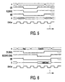
- Figure 5 shows a typical SRAM 16-bit bus write cycle.
- the address is driven onto the address bus ABUS.
- - CS goes active.
- - BLE/ - BHE go active on the same cycle.
- the data are driven onto the data bus DBUS.
- Two clock cycles later, on the rising edge of ClkOut the data are latched into memory by the rising edge of - BLE/ - BHE.
- - CS is also negated on this cycle.
- - WE is negated, terminating the write cycle, and the address bus ABUS and the data bus DBUS change.
- a - BLE/ - BHE bus strobe acts as a data strobe.
- Figure 6 shows a typical DRAM 16-bit read cycle.
- the - RAS to - CAS delay is set to two clock cycles.
- the row address is multiplexed onto pins A17-A6.
- - CS( - RAS) and - OE go active.
- the column address is multiplexed onto the address bus.
- Two clock cycles after - RAS, - BLE/ - BHE go active.
- the DRAM drives the data onto the data bus.
- Figure 7 shows a typical DRAM 16-bit write cycle.
- the register BTMG is set to an access time of two clock cycles.
- the row address is multiplexed onto the pins A17-A6.
- - CS - RAS
- - WE go active, and the data are driven onto the data bus.
- - CS - RAS
- the column address is multiplexed onto the address bus.
- Figure 8 shows a DRAM refresh cycle.
- the strobe - BLE/ - BHE acting as a - CS ( - CAS) strobe, is asserted with - WE and - OE negated.
- a - CS ( - RAS) is asserted for all memory banks configured for DRAMs.
- the - CS ( - RAS) and - BLE/ - BHE( - CAS) are negated.
- a recovery time RT is four clock cycles.
- the shown DRAM refresh cycle is a so-called - CAS before - RAS refresh cycle, in which the unique - CS( - RAS) strobe and global bus strobe - BLE/ - BHE( - CAS) cooperate to perform the refresh cycle.
- a column in the DRAM will be refreshed.
Landscapes
- Engineering & Computer Science (AREA)
- Theoretical Computer Science (AREA)
- Physics & Mathematics (AREA)
- General Engineering & Computer Science (AREA)
- General Physics & Mathematics (AREA)
- Microelectronics & Electronic Packaging (AREA)
- Dram (AREA)
- Microcomputers (AREA)
Description
- The present invention relates to a data processor integrated circuit with a memory interface unit for coupling a microprocessor to a memory external to the microprocessor, and to input/output devices of a memory-mapped type.
- In the
US Patent No. 5,761,478 , a programmable memory interface is disclosed for efficient transfer of different size data between a microprocessor of a given data and address bus width and memory banks of various data and address width, typically differing from the widths of the microprocessor's buses. In the examples given, the microprocessor, which has a 32 bit internal architecture, can execute programming code from 16 or 32 bit wide external memories, and can load and store 8, 16, and 32 bit data units into external memory and convert them into an internally equivalent 32 bit representation. Depending on the widths of the external memory banks, one external pin configures the memory width to 16 or 32 bit, and two sets of memory strobes and one I/O (input/output) strobe allow zero glue logic to two banks of memory and one bank of external peripherals. For 16 or 8 bit memories, one or two of four pins, otherwise all used as strobe-byte enable pins, are used as additional address pins. The behavior of the pins is manipulated according to the contents of certain registers. All memory banks are of the same directly addressable type. What is thus missing but needed is interfacing to mixed types of memory units, i.e., to generic memories such as ROM, SRAM, EPROM, Flash Memory, and memory-mapped I/O-devices on the one hand, and volatile memories such as DRAM which need refreshing on the other hand. - In the
US Patent No. 4,349,870 , a microcomputer with a programmable multifunction port is disclosed. One of a plurality of ports is user programmable by application of specific signals to mode selection pins. The programmable port comprises a number of lines which can be programmed as input or output lines to peripheral equipment, or, alternatively, can be programmed to serve as a bi-directional data bus to external memory. - In the
US Patent No. 4,028, 682 , a circuit is disclosed for selecting the function of connecting contacts on circuit chips. Contacts can be selectively designated as either an input or an output contact. - In the
US Patent No. 5,261,116 , a programmable, expandable controller with flexible I/O is disclosed. An output buffer includes multiplexers which permit either a program counter or a control field to be multiplexed to output pins of a device. When the program counter is multiplexed to the output pins, the programmable controller can address external memory devices. - It is remarked that
US 5530965 describes a microcomputer that may be connected directly to such memories as dynamic and static RAM's and to other peripheral circuits. - It is an object of the invention to provide a data processor with a memory interface unit for flexibly coupling a microprocessor to a plurality of memory banks of different type, notably a mixture of generic type memory banks, such as ROM, EPROM, SRAM, Flash Memory, and memory-mapped I/O devices, and DRAMs.
- It is another object of the invention to flexibly interface memory banks of different sizes, different bus width, different access times, different base addresses in a microprocessor memory space
- It is a further object of the invention to speed up program execution after booting up at a microprocessor reset.
- It is still a further object to flexibly interface directly addressable memory-mapped input/output devices.
- In accordance with the invention, a data processor integrated circuit, such as a microcontroller, with a memory interface unit for coupling a microprocessor to a memory external to the microprocessor is provided, said memory being provided in the form of a plurality of memory banks, each of the memory banks being provided with address lines and data lines, at least a first memory bank of the plurality of memory banks being of a first type which is directly addressable, which first memory bank has a chip select input for selecting the first memory bank, and a second memory bank of the plurality of memory banks being of a second type, which is addressable by a row address and a column address, the row address being validated by a row address strobe at a row address strobe input of the second memory bank, and the column address being validated by a column address strobe at a column address strobe input of the second memory bank, said memory interface unit comprising:
- unique strobes for each of the plurality of memory banks, which unique strobes are programmable in dependence of a type of memory bank to which a particular unique strobe relates, a first strobe of the unique strobes being programmed as a chip select signal which is inputted to the chip select input of the first memory bank, and a second strobe of the unique strobes being programmed as the row address strobe inputted to the row address strobe input of the second memory bank, characterized in that, the first memory bank is a non-volatile memory such as a ROM comprising executable code, located at a hard wired fixed address within the address space, and the second memory bank is volatile memory, preferably of DRAM type, the first and second memory bank being swapped after moving the executable code. Preferably memory-mapped registers are defined in the second memory bank for at least configuring types, base addresses, sizes, bus widths, and access times of the memory banks.
-
-
Figure 1 schematically shows a microcontroller with a memory interface unit which is coupled to a memory. -
Figure 2 is a block diagram of a memory interface unit. -
Figure 3 shows an embodiment of a configuration of a memory interface unit. -
Figure 4 shows a typical SRAM 16-bit bus read cycle. -
Figure 5 shows a typical SRAM 16-bit bus write cycle. -
Figure 6 shows a typical DRAM 16-bit read cycle. -
Figure 7 shows a typical DRAM 16-bit write cycle. -
Figure 8 shows a DRAM refresh cycle. -
Figure 1 schematically shows amicrocontroller 1 with amemory interface unit 2 which is coupled to amemory 3, which comprises a plurality of memory banks of mixed generic and DRAM types. Themicrocontroller 1 further comprises amicroprocessor 4, also indicated with CPU, which is coupled to thememory interface unit 2 for controlling the same when executingprogram code 5 stored in thememory 2, after a microcontroller reset. An address/data/control bus 6 is provided between thememory interface unit 2 and thememory 3. Further shown is aDMA control unit 7 which is coupled to thememory interface unit 2. TheDMA control unit 7 controls a plurality of peripherals (not shown) such as data communication peripherals. The CPU (Central Processing Unit) and the DMA (Direct Memory Access)controller 7 can request access to thebus 6, access being granted on the basis of bus arbitration and priority schemes. Such a bus requesting and granting mechanism is well-known in the art. - In the following description active low signals, as indicated in the drawing with an line above a group of characters, are indicated with the symbol-, preceding the group of characters, i.e., if a group of characters ABC indicates an active high logical signal,- ABC indicates the corresponding active low logical signal.
-
Figure 2 is a block diagram of thememory interface unit 2. Thememory interface unit 2 comprises anaddress selector 20 for selecting a 24 bits CPU address or a 24 bits DMA address on the basis of a granted bus request from the CPU or theDMA controller 6, respectively, bus requesting and granting being controlled by anarbiter 21. Thearbiter 21 is further coupled to a DRAM (Dynamic Random Access Memory)refresh timer 22 for also arbitrating DRAM refresh requests, and to atiming generator 23. Thearbiter 21 controls thetiming generator 23 which provides timing signals TS to a row/column address generator 24 which generates row and column addresses onto external address pins A17-A6 (i.e., 12 bits) from multiplexed CPU or DMA address bit a22-a0 (i.e., 23 bits) during various DRAM CAS (Column Address Strobe) cycles. Thetiming generator 23 further generates global strobe signals to strobe the memory banks included in thememory 3, such global strobe signals including a byte low enable signal -BLE, a byte high enable signal -BHE, an output enable signal - OE, and a write enable signal -WE. An external signal WAIT is available after reset. Achip select decoder 25 is coupled to theaddress selector 20. In the example given, up to a maximum of six memory banks can be selected, six unique programmable strobes -CS0, -CS1,- CS2,- CS3, - CS4, and -CS5 being available from thechip select decoder 25 for selecting each memory bank. A unique programmable strobe is physically connected to a chip select pin- CS of a generic memory device such as an ROM or SRAM device, or to a -RAS pin of a DRAM device, an is programmed accordingly. Thechip select decoder 25 compares the most significant address bits of all memory addresses to base addresses, i.e., start addresses in a microprocessor memory space, of the maximally memory banks, and asserts the -CS pin for that bank which matches. In the example given, memory bank addresses are on 4 KByte boundary, so a maximum of 12 bits need to be compared only, namely the most significant address bits, indicated by a23-a12. DRAM logical address bits a22-a0 are multiplexed onto address pins A17-A6 during the row and column phases by row/column address multiplexing. Generic memory logical addresses, a19-a0, appear on external address pins A19-A0 directly. Correct read/write bus cycle timing for each bank, programmed in a bank's timing register, is applied via thetiming generator 23 whenever the bank is selected. Thememory interface unit 2 uses five special function registers and twenty memory mapped registers, which will be described in the following. -
Figure 3 shows an embodiment of a configuration of thememory interface unit 2. In the example given, thememory 3 has four memory banks, aROM memory bank 30 of 128Kx8, i.e., 128 KBytes with a data bus width of 8 bits, indicated by D7-D0, aDRAM memory bank 31 of 256Kx16, i.e., 512 KBytes of memory with a data bus width of 16 bits, indicated by D15-D0, a furtherDRAM memory bank 32 of 1Mx16, i.e., 16 MBytes of memory with a data bus of 16 bits, and anSRAM memory bank 33 of 2Kx16, i.e., 4 KBytes of memory with a data bus width of 16 bits. Thememory bank 30, also being referred to as bank-0, comprises program code and starts at a hard wired fixed base address 000000h in the microprocessor's memory space, 'h' indicating a hexadecimal address notation. Thememory banks memory interface 2 is configured to meet all type, size, base address, width, and timing requirements of the memory banks. Further shown inFigure 3 are an external address bus ABUS, an external data bus DBUS, and an external control bus CBUS. The memory interface chip select signals - CSO, - CS1, - CS2, and -CS3 are connected to the chipselect input 34 of theROM 30, to the rowaddress strobe input 35 of theDRAM 31, to the rowaddress strobe input 36 of theDRAM 32, and to the chipselect input 37 of theSRAM 33, respectively. As regards theDRAMs memory 3.

memory interface unit 2, a bus timing register high BTRH, a bus timing register low BTRL, a memory mapped register base address high MRBH, a memory mapped register base address low BRBL, and a memory interface general configuration register MICFG. The register MRBH contains the high order byte of the MMR base address, address bits A23-A16, indicated by MA23-MA16. The register MRBL contains the lowest four bits of the MMR (memory mapped register) base address, address bits A15-A12, indicated by MA15, MA14, MA13, and MA12. The LSB (least significant bit) is MRBE, a logic "0" disabling access to the MMRs, and a logic "1" enabling access to the MMRs. The MMR base address is formed by the twelve bits MA23-MA12, padded by twelve zero bits, and is compared to address bits a23-a12 from the CPU to initiate MMR accesses. The register MICFG contains only one functional bit, the bit CLKOE (Clock Output Enable) which is set at a microprocessor reset.Table II B0CFG R/ W 8 280h MIF Bank 0 Config B0AM R/ W 8 281h MIF Bank 0 Base Address B0TMG R/ W 8 282h MIF Bank 0 Timing Params B1CFG R/ W 8 284h MIF Bank 1 Config B1AM R/ W 8 285h MIF Bank 1 Base Address B1TMG R/ W 8 286h MIF Bank 1 Timing Params B2CFG R/ W 8 288h MIF Bank 2 Config B2AM R/ W 8 289h MIF Bank 2 Base Address B2TMG R/ W 8 28Ah MIF Bank 2 Timing Params B3CFG R/ W 8 28Ch MIF Bank 3 Config B3AM R/ W 8 28Dh MIF Bank 3 Base Address B3TMG R/ W 8 28Eh MIF Bank 3 Timing Params B4CFG R/ W 8 290h MIF Bank 4 Config B4AM R/ W 8 291h MIF Bank 4 Base Address B4TMG R/ W 8 292h MIF Bank 4 Timing Params B5CFG R/ W 8 294h MIF Bank 5 Config B5AM R/ W 8 295h MIF Bank 5 Base Address B5TMG R/ W 8 296h MIF Bank 5 Timing Params MBCL R/ W 8 2Beh MIF Memory Bank Configuration Lock Register RFSH R/ W 8 2BFh MIF Refresh Control - Table II shows a set of memory-mapped memory interface unit registers. For each memory bank there are three registers, a bank-i configuration register BiCFG, a bank-i base address/DRAM address multiplexer control register BiAM, and a bank-i timing register BiTMG, i=0, 1, 2, 3,4, and 5. There are two further registers, a memory bank configuration lock register MCBL and a refresh control register RFSH. Bits of the configuration register BiCFG determine whether a bank is code and/or data memory access enabled, and determine a bank's bus width, 8 or 16 bit, type, generic or DRAM, and size, between 64KBytes and 8MBytes for bank-0 and between 4 KBytes and 8MBytes for bank-1 to bank-5. Bits of the BiAM register have different functions, depending on a memory bank's type and size. For a generic type of memory bank of 64KBytes or higher, the bank's base address is formed by the bits of the MRBH register and the four MSBs (Most Significant Bits) of the BiAM register, for a generic type of memory bank of 32KBytes or smaller, all bits of the BiAM register for the bank's base address, and for a DRAM memory bank, the six MSBs of the BiAM register are used as address bits a23-a18 of the base address. Then, the two least significant bits of the BiAM are row/column address multiplexer control bits BiMX1 and BiMX0, to be described in more detail in relation to
Figure 8 . Bits of the BiTMG register determine - CS to - WE delay for generic type memory banks, -RAS to - CAS delay for DRAM memory banks, in clock cycles, and other access timing parameters. The MCBL register's MSB enables or disables memory bank-0/bank-1 swapping, bank swapping being disables upon reset, and further bits determine configuration locking/unlocking of the different memory banks. Bits of the RFSH register enable/disable therefresh timer 22, and determine a seven-bit time constant for therefresh timer 22. The timer will time out once every 8xRFSH[6:0] system clock cycles, [6:0] indicating the seven LSBs of the RFSH register. On each refresh timer time out, a request is sent to thearbiter 21.Table III Bank 0 Size and Address Range select B0CFG[3] B0CFG[2] B0CFG[1] B0CFG[0] Bank 0 Size Bank 0 Address Range 1 0 0 0 64K Bytes 000000h- 00FFFFh 1 0 0 1 128K Bytes 000000h- 01FFFFh 1 0 1 0 256K Bytes 000000h- 03FFFFh 1 0 1 1 512K Bytes 000000h- 07FFFFh 1 1 0 0 1M Bytes 000000h- 0FFFFFh 1 1 0 1 2M Bytes 000000h- 1FFFFFh 1 1 1 0 3M Bytes 000000h- 3FFFFFh 1 1 1 1 4M Bytes 000000h-7FFFFh - Table III shows bank-0 size and address range selection. Bank-0's base address is hard wired and is set to 000000h. Shown are bit setting of the B0CFG register to set the bank's size and address range. Bank-0 is the boot bank. Bank-0 is always enabled for code memory access and can be enabled for data memory access.

- Table IV shows bank 1-5 size and base address selection. Bank-1 to bank-5 size and address selection is determined by bit settings of the BiCFG register, the MRB register, and the BiAM register, as shown, lower address bits being zero, as the case may be. Banks bank-1 to bank-5 can be configured as either a generic memory or a DRAM. After boot up, application code stored in bank-0, a ROM, will be written into bank-1, preferably a DRAM memory bank, for subsequent execution. After bank-0/bank-1 swapping, the application code can still be accessed from base address 000000h. Bank swapping also allows interrupt vectors, which are in low memory, to be write accessed. The advantage of such a bank swapping is that the application code is executed substantially faster.
Table V BiMX1 and BiMX0 Configuration Data Bus Width Number of Bytes BiMX1 BiMX0 Address Mux Scheme 8-Bit Bus 256kBytes 00 A 1 Mbytes 01 B 2Mbytes 10 C 8Mbytes 11 D 16- Bit Bus 256K deep (512 kB total) 00 E 1M deep (2Mbytes total) 01 F 4M deep (8Mbytes total) 10 G Reserved 11 - - Table V shows a configuration of row/column multiplexer bits for specific DRAMs. The two least significant bits of the BiAM register, the row/column address multiplexer control bits BiMX1 and BiMX0, determine multiplex scheme A through G for various data bus width and memory sizes.
Table VI DRAM Row and Column Address Multiplexing Address Mux Scheme Address Pin A17 A16 A15 A14 A13 A12 A11 A10 A9 A8 A7 A6 A Row a17 a16 a15 a14 a13 a12 a11 a10 a9 u u u Column a8 a7 a6 a5 a4 a3 a2 a1 a0 u u u B Row a17 a16 a15 a14 a13 a12 a11 a10 a9 a8 u u Column a18 a7 a6 a5 a4 a3 a2 a1 a0 a19 u u C Row a17 a16 a15 a14 a13 a12 a11 a10 a9 a8 a7 u Column a18 a20 a6 a5 a4 a3 a2 a1 a0 a19 a21 u D Row a17 a16 a15 a14 a13 a12 a11 a10 a9 a8 a7 a6 Column a18 a20 a22 a5 a4 a3 a2 a1 a0 a19 a21 u E Row a17 a16 a15 a14 a13 a12 a11 a10 a9 u u u Column a8 a7 a6 a5 a4 a3 a2 a1 a18 u u u F Row a17 a16 a15 a14 a13 a12 a11 a10 a9 a8 u u Column a8 a7 a6 a5 a4 a3 a2 a1 a18 a20 u u G Row a17 a16 a15 a14 a13 a12 a11 a10 a9 a8 a7 u Column a8 a7 a6 a5 a4 a3 a2 a1 a18 a20 a22 u Note 1 use Table 3-6 to determine Address Mux Scheme and [BiMX1 BiMX0] values Note 2 During RAS, the logical address and the address pin are always identical - Table VI shows the DRAM row and column address multiplexing schemes A through G in relation to the assignment of logical addresses a23-a0 to the external pins A17-A6 during the row and column address phases of a DRAM access. 'u' indicating unused pins. In the example given, so-called - CAS before -RAS refresh is performed.
- With the definition and description of all necessary memory interface registers above, the embodiment of the configuration of the
memory interface unit 2 as shown inFigure 3 will now be described in more detail. -
Bank 30, the boot bank, andbank 31, the first DRAM bank, are first configured after a reset.Bank 30 has address range 000000h-01FFFFh as indicated by the register B0CFG described inFigure 6 .Bank 31 has address range 100000h-17FFFFh as indicated by the registers B1CFG, MRB, and B1AM described in Table IV. Similarly, sizes and ranges ofbanks - After final bank swapping, the address ranges and sizes of
bank 30 andbank 31 are interchanged, the then address range ofbank 31, 100000h-11FFFFh activating the ROM on - CS0, and the then address range 000000h-07ffffh activating the DRAM on - CS1. Before bank swapping the banks are configured as follows. The MRBH register is set to FFh, indicating MMR base address bits a23-16. The MRBL register is set to F1h, bits [3:1] of the MRBL register being don't cares, and MMR access is enabled. Then, the MCBL register is set to lock the registers forbanks bank 30 is data access disabled.Bank 31 is set to two cycle -RAS to- CAS delay, and to two cycle delay from data strobes low to sampling of the data bus or latching data into memory, by appropriate settings of the B1TMG register. The B1CFG register is set to code and data enable thememory bank 31, and to indicate a DRAM type memory of size 512KBytes of 16 bit words. The B1AM register is set to 10h, indicating abank 31 base address 100000h and indicating multiplexing scheme E as described inFigures 8 and 9.Banks DRAMs ROM 30 to theDRAM 31. Then, bank swapping is performed. - The timing examples of
Figures 4-7 illustrate the effects of memory interface settings, particularly the effects of the settings of the register BiTMG. -
Figure 4 shows a typical SRAM 16-bit bus read cycle. Access time is set to 2 clock cycles. On a rising edge of ClkOut, the address is driven onto the address bus ABUS. One clock cycle after the address changes, - CS and - OE go active. - BLE/- BHE go active on the same cycle. The data bus DBUS is sampled on the rising edge of ClkOut, 2 cycles later. At this point the read cycle is terminated as - CS, - BLE/- BLH, and - OE are negated, and the address bus ABUS and the data bus DBUS begin to change. -
Figure 5 shows a typical SRAM 16-bit bus write cycle. On the rising edge of ClkOut, the address is driven onto the address bus ABUS. One clock cycle later, -CS goes active. -BLE/- BHE go active on the same cycle. At this point, the data are driven onto the data bus DBUS. Two clock cycles later, on the rising edge of ClkOut, the data are latched into memory by the rising edge of -BLE/-BHE. -CS is also negated on this cycle. One clock cycle later, - WE is negated, terminating the write cycle, and the address bus ABUS and the data bus DBUS change. For a generic type of memory bank, such as an SRAM, a -BLE/- BHE bus strobe acts as a data strobe. -
Figure 6 shows a typical DRAM 16-bit read cycle. In the BTMG register, the - RAS to - CAS delay is set to two clock cycles. On the rising edge of ClkOut, the row address is multiplexed onto pins A17-A6. One clock cycle later, -CS(-RAS) and -OE go active. One clock cycle after RAS, the column address is multiplexed onto the address bus. Two clock cycles after -RAS, -BLE/-BHE go active. After the DRAM's access time has elapsed, the DRAM drives the data onto the data bus. One clock cycle before the negation of -BLE/-BHE (-CAS) are asserted, the data bus is sampled on the rising edge of -BLE/-BHE, -OE is also negated, and the address bus changes. For a DRAM type of memory, the -BLE/-BHE bus strobe acts as a -CAS strobe. -
Figure 7 shows a typical DRAM 16-bit write cycle. The register BTMG is set to an access time of two clock cycles. On a rising edge of ClkOut, the row address is multiplexed onto the pins A17-A6. One clock cycle later, -CS (-RAS) and -WE go active, and the data are driven onto the data bus. One clock cycle after -CS (-RAS), the column address is multiplexed onto the address bus. Two clock cycles after -CS (-RAS), because the -RAS to -CAS delay is two clock cycles, -BLE/-BHE go active. Two clock cycles after -BLE/-BHE, because access time is two clock cycles, the data are latched into memory by the rising edge of -BLE/-BHE, and -CS (-RAS) is negated simultaneously. Write data will remain valid for another clock cycle. One clock cycle after -CS (-RAS) goes high, the address bus changes, and the write cycle is terminated by the rising edge of -WE. -
Figure 8 shows a DRAM refresh cycle. First the strobe -BLE/-BHE, acting as a -CS (-CAS) strobe, is asserted with -WE and -OE negated. One clock cycle later, a -CS (-RAS) is asserted for all memory banks configured for DRAMs. Then, for all DRAMs, after a given number of clock cycles after the falling edge of -CS (- RAS), the -CS (-RAS) and -BLE/-BHE(-CAS) are negated. In the example given, a recovery time RT is four clock cycles. The shown DRAM refresh cycle is a so-called -CAS before -RAS refresh cycle, in which the unique -CS(-RAS) strobe and global bus strobe -BLE/-BHE(-CAS) cooperate to perform the refresh cycle. At every occurrence of the combined -CS(-RAS) and -BLE/-BHE(-CAS) strobes, a column in the DRAM will be refreshed. - In view of the foregoing it will be evident to a person skilled in the art that various modifications may be made as hereinafter defined by the appended claims and that the invention is thus not limited to the examples provided.
Claims (11)
- A data processor integrated circuit (1) comprising a microprocessor (4) and memory interface unit (2) for coupling the microprocessor (4) to a memory (3) external to the microprocessor (4), said memory (3) being provided in the form of a plurality of memory banks (30,31,32,33), each of the memory banks being provided with address lines (A16-A0)and data lines(D15-D0), at least a first memory bank (30) of the plurality of memory banks being of a first type which is directly addressable, which first memory (30) bank has a chip select input (-CS) for selecting the first memory bank (30), and a second memory bank (31) of the plurality of memory banks being of a second type, which is addressable by a row address and a column address, the row address being validated by a row address strobe (-RAS) at a row address strobe input of the second memory bank, and the column address being validated by a column address strobe (-CAS) at a column address strobe input of the second memory bank, said memory interface unit comprising:unique strobes (-CS5--CS0) for each of the plurality of memory banks(30,31,32,33), which unique strobes are programmable in dependence of a type of memory bank to which a particular unique strobe relates, a first strobe (-CS0) of the unique strobes being programmed as a chip select signal which is inputted to the chip select input of the first memory bank, and a second strobe (-CS1) of the unique strobes being programmed as the row address strobe inputted to the row address strobe input of the second memory bank(31),characterized in that the first memory bank (30) is of non-volatile type in which executable code is stored including boot up code, and after execution of the boot up code at a microprocessor reset the executable code is moved from the first memory bank to the second memory bank(31) and that after moving the executable code the first and second memory banks are swapped so that the executable code is executable from the same base address as before swapping.
- A data processor integrated circuit of claim 1, comprising first configuration means (BiCFG) for configuring types of the memory banks.
- A data processor integrated circuit of claim 1, comprising second configuration means (BiAM) for configuring base addresses and sizes of the memory banks, within an addressable range of the microprocessor.
- A data processor integrated circuit of claim 1, comprising third configuration means for configuring bus widths of the memory banks.
- A data processor integrated circuit of claim 1, comprising fourth configuration (BiCFG) means for configuring access times of the memory banks.
- A data processor integrated circuit of claim 5, wherein the memory bank to be configured is a memory bank (30) of the first type and an access time is configured as being a multiple of microprocessor clock cycles between asserting a data strobe (-BLE/-BLH) to the memory bank (30) of the first type and sampling of a data bus, in case of a read operation, and between asserting the data strobe and latching of data into the memory bank, in case of a write operation.
- A data processor integrated circuit of claim 5, wherein the memory bank to be configured is a memory bank of the second type (31) and an access time is configured as a being a multiple of microprocessor clock cycles between asserting a row address strobe (-RAS) and a column address strobe(-CAS).
- A data processor integrated circuit of claim 1, for further coupling the microprocessor to an input/output device of a directly addressable memory-mapped input/output type.
- A data processor integrated circuit of claim 1, wherein configuration means including a selection of configuring types, base addresses, sizes, bus widths, and access times of the memory banks are comprised in the second memory bank in the form of a set of memory-mapped read-write registers.
- A data processor integrated circuit of claim 1, wherein a global bus strobe (-BLE/-BLH) is asserted which acts as a data strobe for a memory bank of the first type and which acts as a column address (-CAS) strobe for a memory bank of the second type.
- A memory interface unit (2) for coupling a microprocessor (4) to a memory external (3) to the microprocessor (4), said memory (3) being provided in the form of a plurality of memory banks (30,31,32,33), each of the memory banks being provided with address lines (A16-A0) and data lines (D15-D0), at least a first memory bank (30) of the plurality of memory banks being of a first type which is directly addressable, which first memory bank (30) has a chip select input (-CS) for selecting the first memory bank (30), and a second memory bank (31) of the plurality of memory banks being of a second type, which is addressable by a row address and a column address, the row address being validated by a row address strobe (-RAS) at a row address strobe input of the second memory bank, and the column address being validated by a column address strobe (-CAS) at a column address strobe input of the second memory bank, said memory interface unit comprising:unique strobes (-CS5- -CS0) for each of the plurality of memory banks(30,31,32,33), which unique strobes are programmable in dependence of a type of memory bank to which a particular unique strobe relates, a first strobe (-CS0) of the unique strobes being programmed as a chip select signal which is inputted to the chip select input of the first memory bank(30), and a second strobe (-CS1) of the unique strobes being programmed as the row address strobe inputted to the row address strobe input of the second memory bank(31),characterized in that the first memory bank (30) is of non-volatile type in which executable code is stored including boot up code, and after execution of the boot up code at a microprocessor reset the executable code is moved from the first memory bank to the second memory bank(31) and that after moving the executable code the first and second memory banks are swapped so that the executable code is executable from the same base address as before swapping.
Applications Claiming Priority (3)
| Application Number | Priority Date | Filing Date | Title |
|---|---|---|---|
| US198925 | 1994-02-18 | ||
| US09/198,925 US6601130B1 (en) | 1998-11-24 | 1998-11-24 | Memory interface unit with programmable strobes to select different memory devices |
| PCT/EP1999/008614 WO2000031646A2 (en) | 1998-11-24 | 1999-11-03 | Data processor integrated circuit with a memory interface unit with programmable strobes to select different memory devices |
Publications (2)
| Publication Number | Publication Date |
|---|---|
| EP1055178A2 EP1055178A2 (en) | 2000-11-29 |
| EP1055178B1 true EP1055178B1 (en) | 2009-02-11 |
Family
ID=22735474
Family Applications (1)
| Application Number | Title | Priority Date | Filing Date |
|---|---|---|---|
| EP99964480A Expired - Lifetime EP1055178B1 (en) | 1998-11-24 | 1999-11-03 | Data processor integrated circuit with a memory interface unit with programmable strobes to select different memory devices |
Country Status (6)
| Country | Link |
|---|---|
| US (1) | US6601130B1 (en) |
| EP (1) | EP1055178B1 (en) |
| JP (1) | JP2002530777A (en) |
| KR (1) | KR100679758B1 (en) |
| DE (1) | DE69940397D1 (en) |
| WO (1) | WO2000031646A2 (en) |
Families Citing this family (20)
| Publication number | Priority date | Publication date | Assignee | Title |
|---|---|---|---|---|
| JP2001290697A (en) * | 2000-04-06 | 2001-10-19 | Hitachi Ltd | Information processing system |
| US6792499B1 (en) * | 2000-11-14 | 2004-09-14 | Cypress Semiconductor Corp. | Dynamic swapping of memory bank base addresses |
| JP2002342256A (en) * | 2001-05-14 | 2002-11-29 | Hitachi Ltd | Data processor and data table updating method |
| US6721227B2 (en) * | 2002-02-11 | 2004-04-13 | Micron Technology, Inc. | User selectable banks for DRAM |
| US6981122B2 (en) * | 2002-09-26 | 2005-12-27 | Analog Devices, Inc. | Method and system for providing a contiguous memory address space |
| US6876563B1 (en) * | 2002-12-20 | 2005-04-05 | Cypress Semiconductor Corporation | Method for configuring chip selects in memories |
| US20040143696A1 (en) * | 2003-01-21 | 2004-07-22 | Francis Hsieh | Data storage system for fast booting of computer |
| US20050041453A1 (en) * | 2003-08-22 | 2005-02-24 | Brazis Paul W. | Method and apparatus for reading and writing to solid-state memory |
| US7564735B2 (en) * | 2006-07-05 | 2009-07-21 | Qimonda Ag | Memory device, and method for operating a memory device |
| US7913022B1 (en) * | 2007-02-14 | 2011-03-22 | Xilinx, Inc. | Port interface modules (PIMs) in a multi-port memory controller (MPMC) |
| US7711907B1 (en) | 2007-02-14 | 2010-05-04 | Xilinx, Inc. | Self aligning state machine |
| US7720636B1 (en) | 2007-02-14 | 2010-05-18 | Xilinx, Inc. | Performance monitors (PMs) for measuring performance in a system and providing a record of transactions performed |
| US8479124B1 (en) | 2007-02-14 | 2013-07-02 | Xilinx, Inc. | Graphical user interface (GUI) including input files with information that determines representation of subsequent content displayed by the GUI |
| CN101464845B (en) * | 2009-01-09 | 2012-09-05 | 威盛电子股份有限公司 | Prefetch device, prefetch system and data prefetch method for bus system |
| US8971094B2 (en) * | 2011-09-16 | 2015-03-03 | Inphi Corporation | Replacement of a faulty memory cell with a spare cell for a memory circuit |
| US9158726B2 (en) | 2011-12-16 | 2015-10-13 | Inphi Corporation | Self terminated dynamic random access memory |
| US9069717B1 (en) | 2012-03-06 | 2015-06-30 | Inphi Corporation | Memory parametric improvements |
| US10452561B2 (en) | 2016-08-08 | 2019-10-22 | Raytheon Company | Central processing unit architecture and methods for high availability systems |
| TWI692759B (en) * | 2019-05-15 | 2020-05-01 | 瑞昱半導體股份有限公司 | Method for simultaneously accessing first dram device and second dram device and associated memory controller |
| US11798604B2 (en) * | 2021-09-01 | 2023-10-24 | Dell Products L.P. | Memory architecture having ranks with variable data widths |
Family Cites Families (13)
| Publication number | Priority date | Publication date | Assignee | Title |
|---|---|---|---|---|
| DE2364253A1 (en) | 1973-12-22 | 1975-06-26 | Olympia Werke Ag | CIRCUIT ARRANGEMENT FOR MICROPROGRAMMED DATA PROCESSING DEVICES |
| US4349870A (en) | 1979-09-05 | 1982-09-14 | Motorola, Inc. | Microcomputer with programmable multi-function port |
| US5261116A (en) | 1986-07-02 | 1993-11-09 | Advanced Micro Devices, Inc. | Programmable, expandable controller with flexible I/O |
| US4903197A (en) * | 1987-02-27 | 1990-02-20 | Bull Hn Information Systems Inc. | Memory bank selection arrangement generating first bits identifying a bank of memory and second bits addressing identified bank |
| US5307320A (en) | 1992-09-23 | 1994-04-26 | Intel Corporation | High integration DRAM controller |
| JPH0845269A (en) * | 1994-07-27 | 1996-02-16 | Hitachi Ltd | Semiconductor memory device |
| US5784700A (en) | 1994-12-12 | 1998-07-21 | Texas Instruments Incorporated | Memory interface with address shift for different memory types |
| JPH09180431A (en) | 1995-12-26 | 1997-07-11 | Nec Niigata Ltd | Single in-line memory module system |
| US5715207A (en) | 1996-03-28 | 1998-02-03 | International Business Machines Corporation | Memory presence and type detection using multiplexed memory line function |
| KR100252254B1 (en) * | 1996-06-26 | 2000-04-15 | 윤종용 | Interoperable computer system of heterogeneous memory modules |
| JP3761635B2 (en) * | 1996-07-12 | 2006-03-29 | 株式会社ダックス | Memory board, memory access method, and memory access device |
| US5781492A (en) * | 1997-02-04 | 1998-07-14 | Advanced Micro Devices, Inc. | System and method for mapping memory to DRAM after system boot from non-volatile memory |
| US6023750A (en) * | 1997-03-07 | 2000-02-08 | Advanced Micro Devices, Inc. | Microcontroller having dedicated hardware for memory address space expansion via auxilliary address signal generation |
-
1998
- 1998-11-24 US US09/198,925 patent/US6601130B1/en not_active Expired - Lifetime
-
1999
- 1999-11-03 EP EP99964480A patent/EP1055178B1/en not_active Expired - Lifetime
- 1999-11-03 DE DE69940397T patent/DE69940397D1/en not_active Expired - Lifetime
- 1999-11-03 JP JP2000584395A patent/JP2002530777A/en not_active Withdrawn
- 1999-11-03 WO PCT/EP1999/008614 patent/WO2000031646A2/en not_active Ceased
- 1999-11-03 KR KR1020007008064A patent/KR100679758B1/en not_active Expired - Fee Related
Also Published As
| Publication number | Publication date |
|---|---|
| KR20010034334A (en) | 2001-04-25 |
| US6601130B1 (en) | 2003-07-29 |
| WO2000031646A3 (en) | 2000-10-05 |
| EP1055178A2 (en) | 2000-11-29 |
| DE69940397D1 (en) | 2009-03-26 |
| JP2002530777A (en) | 2002-09-17 |
| WO2000031646A2 (en) | 2000-06-02 |
| KR100679758B1 (en) | 2007-02-07 |
Similar Documents
| Publication | Publication Date | Title |
|---|---|---|
| KR100679758B1 (en) | Memory Interface Units and Data Processor Integrated Circuits Including the Same | |
| US5226134A (en) | Data processing system including a memory controller for direct or interleave memory accessing | |
| US20040098549A1 (en) | Apparatus and methods for programmable interfaces in memory controllers | |
| US6330647B1 (en) | Memory bandwidth allocation based on access count priority scheme | |
| US5546548A (en) | Arbiter and arbitration process for a dynamic and flexible prioritization | |
| US5129069A (en) | Method and apparatus for automatic memory configuration by a computer | |
| EP0473275B1 (en) | Memory control unit and memory unit | |
| US10403333B2 (en) | Memory controller with flexible address decoding | |
| KR860000541B1 (en) | Refresh circuit of dynamic memory | |
| US6047347A (en) | Computer system with programmable bus size | |
| US20020032829A1 (en) | Microprocessor memory device controller | |
| US5574866A (en) | Method and apparatus for providing a data write signal with a programmable duration | |
| US5784642A (en) | System for establishing a transfer mode between system controller and peripheral device | |
| US5724604A (en) | Data processing system for accessing an external device and method therefor | |
| US5638520A (en) | Method and apparatus for distributing bus loading in a data processing system | |
| US6622203B2 (en) | Embedded memory access method and system for application specific integrated circuits | |
| JPS61112221A (en) | Multi-writable initialization word for writable read-only-memory | |
| JPS629456A (en) | Data transfer unit | |
| US5748982A (en) | Apparatus for selecting a user programmable address for an I/O device | |
| US5901298A (en) | Method for utilizing a single multiplex address bus between DRAM, SRAM and ROM | |
| US5781492A (en) | System and method for mapping memory to DRAM after system boot from non-volatile memory | |
| US5630098A (en) | System and method for interleaving memory addresses between memory banks based on the capacity of the memory banks | |
| US5271098A (en) | Method and apparatus for use of expanded memory system (EMS) to access cartridge memory | |
| EP0798644A2 (en) | Method and apparatus for accessing a chip-selectable device in a data processing system | |
| US5748922A (en) | Method and apparatus for reading data from a write only port |
Legal Events
| Date | Code | Title | Description |
|---|---|---|---|
| PUAI | Public reference made under article 153(3) epc to a published international application that has entered the european phase |
Free format text: ORIGINAL CODE: 0009012 |
|
| AK | Designated contracting states |
Kind code of ref document: A2 Designated state(s): AT BE CH CY DE DK ES FI FR GB GR IE IT LI LU MC NL PT SE |
|
| 17P | Request for examination filed |
Effective date: 20010405 |
|
| RBV | Designated contracting states (corrected) |
Designated state(s): DE FR GB IT |
|
| 17Q | First examination report despatched |
Effective date: 20061204 |
|
| RAP1 | Party data changed (applicant data changed or rights of an application transferred) |
Owner name: NXP B.V. |
|
| GRAP | Despatch of communication of intention to grant a patent |
Free format text: ORIGINAL CODE: EPIDOSNIGR1 |
|
| GRAS | Grant fee paid |
Free format text: ORIGINAL CODE: EPIDOSNIGR3 |
|
| GRAS | Grant fee paid |
Free format text: ORIGINAL CODE: EPIDOSNIGR3 |
|
| GRAA | (expected) grant |
Free format text: ORIGINAL CODE: 0009210 |
|
| AK | Designated contracting states |
Kind code of ref document: B1 Designated state(s): DE FR GB IT |
|
| REG | Reference to a national code |
Ref country code: GB Ref legal event code: FG4D |
|
| REF | Corresponds to: |
Ref document number: 69940397 Country of ref document: DE Date of ref document: 20090326 Kind code of ref document: P |
|
| PLBE | No opposition filed within time limit |
Free format text: ORIGINAL CODE: 0009261 |
|
| STAA | Information on the status of an ep patent application or granted ep patent |
Free format text: STATUS: NO OPPOSITION FILED WITHIN TIME LIMIT |
|
| 26N | No opposition filed |
Effective date: 20091112 |
|
| PGFP | Annual fee paid to national office [announced via postgrant information from national office to epo] |
Ref country code: FR Payment date: 20091123 Year of fee payment: 11 |
|
| PGFP | Annual fee paid to national office [announced via postgrant information from national office to epo] |
Ref country code: DE Payment date: 20101027 Year of fee payment: 12 |
|
| PG25 | Lapsed in a contracting state [announced via postgrant information from national office to epo] |
Ref country code: IT Free format text: LAPSE BECAUSE OF FAILURE TO SUBMIT A TRANSLATION OF THE DESCRIPTION OR TO PAY THE FEE WITHIN THE PRESCRIBED TIME-LIMIT Effective date: 20090211 |
|
| REG | Reference to a national code |
Ref country code: FR Ref legal event code: ST Effective date: 20110801 |
|
| PG25 | Lapsed in a contracting state [announced via postgrant information from national office to epo] |
Ref country code: FR Free format text: LAPSE BECAUSE OF NON-PAYMENT OF DUE FEES Effective date: 20101130 |
|
| REG | Reference to a national code |
Ref country code: DE Ref legal event code: R119 Ref document number: 69940397 Country of ref document: DE Effective date: 20120601 |
|
| PG25 | Lapsed in a contracting state [announced via postgrant information from national office to epo] |
Ref country code: DE Free format text: LAPSE BECAUSE OF NON-PAYMENT OF DUE FEES Effective date: 20120601 |
|
| PGFP | Annual fee paid to national office [announced via postgrant information from national office to epo] |
Ref country code: GB Payment date: 20141028 Year of fee payment: 16 |
|
| GBPC | Gb: european patent ceased through non-payment of renewal fee |
Effective date: 20151103 |
|
| PG25 | Lapsed in a contracting state [announced via postgrant information from national office to epo] |
Ref country code: GB Free format text: LAPSE BECAUSE OF NON-PAYMENT OF DUE FEES Effective date: 20151103 |