EP1054491A2 - Gallium nitride based semiconductor light emitting device - Google Patents
Gallium nitride based semiconductor light emitting device Download PDFInfo
- Publication number
- EP1054491A2 EP1054491A2 EP00110206A EP00110206A EP1054491A2 EP 1054491 A2 EP1054491 A2 EP 1054491A2 EP 00110206 A EP00110206 A EP 00110206A EP 00110206 A EP00110206 A EP 00110206A EP 1054491 A2 EP1054491 A2 EP 1054491A2
- Authority
- EP
- European Patent Office
- Prior art keywords
- layer
- waveguide
- based semiconductor
- type cladding
- cladding layer
- Prior art date
- Legal status (The legal status is an assumption and is not a legal conclusion. Google has not performed a legal analysis and makes no representation as to the accuracy of the status listed.)
- Withdrawn
Links
- 239000004065 semiconductor Substances 0.000 title claims abstract description 27
- 229910002601 GaN Inorganic materials 0.000 title claims description 28
- JMASRVWKEDWRBT-UHFFFAOYSA-N Gallium nitride Chemical compound [Ga]#N JMASRVWKEDWRBT-UHFFFAOYSA-N 0.000 title claims description 11
- 238000005253 cladding Methods 0.000 claims abstract description 44
- 239000000758 substrate Substances 0.000 claims abstract description 8
- 230000001902 propagating effect Effects 0.000 claims abstract description 5
- 238000000151 deposition Methods 0.000 claims description 2
- 238000009826 distribution Methods 0.000 description 7
- 230000000644 propagated effect Effects 0.000 description 5
- 150000001875 compounds Chemical class 0.000 description 4
- 230000003287 optical effect Effects 0.000 description 4
- 229910052594 sapphire Inorganic materials 0.000 description 4
- 239000010980 sapphire Substances 0.000 description 4
- 238000010586 diagram Methods 0.000 description 3
- 238000004519 manufacturing process Methods 0.000 description 3
- 238000000034 method Methods 0.000 description 3
- 230000008878 coupling Effects 0.000 description 2
- 238000010168 coupling process Methods 0.000 description 2
- 238000005859 coupling reaction Methods 0.000 description 2
- 239000013078 crystal Substances 0.000 description 1
- 239000002019 doping agent Substances 0.000 description 1
- 230000002349 favourable effect Effects 0.000 description 1
Images


Classifications
-
- H—ELECTRICITY
- H01—ELECTRIC ELEMENTS
- H01S—DEVICES USING THE PROCESS OF LIGHT AMPLIFICATION BY STIMULATED EMISSION OF RADIATION [LASER] TO AMPLIFY OR GENERATE LIGHT; DEVICES USING STIMULATED EMISSION OF ELECTROMAGNETIC RADIATION IN WAVE RANGES OTHER THAN OPTICAL
- H01S5/00—Semiconductor lasers
- H01S5/30—Structure or shape of the active region; Materials used for the active region
- H01S5/32—Structure or shape of the active region; Materials used for the active region comprising PN junctions, e.g. hetero- or double- heterostructures
- H01S5/323—Structure or shape of the active region; Materials used for the active region comprising PN junctions, e.g. hetero- or double- heterostructures in AIIIBV compounds, e.g. AlGaAs-laser, InP-based laser
- H01S5/32308—Structure or shape of the active region; Materials used for the active region comprising PN junctions, e.g. hetero- or double- heterostructures in AIIIBV compounds, e.g. AlGaAs-laser, InP-based laser emitting light at a wavelength less than 900 nm
- H01S5/32341—Structure or shape of the active region; Materials used for the active region comprising PN junctions, e.g. hetero- or double- heterostructures in AIIIBV compounds, e.g. AlGaAs-laser, InP-based laser emitting light at a wavelength less than 900 nm blue laser based on GaN or GaP
-
- H—ELECTRICITY
- H01—ELECTRIC ELEMENTS
- H01S—DEVICES USING THE PROCESS OF LIGHT AMPLIFICATION BY STIMULATED EMISSION OF RADIATION [LASER] TO AMPLIFY OR GENERATE LIGHT; DEVICES USING STIMULATED EMISSION OF ELECTROMAGNETIC RADIATION IN WAVE RANGES OTHER THAN OPTICAL
- H01S5/00—Semiconductor lasers
- H01S5/20—Structure or shape of the semiconductor body to guide the optical wave ; Confining structures perpendicular to the optical axis, e.g. index or gain guiding, stripe geometry, broad area lasers, gain tailoring, transverse or lateral reflectors, special cladding structures, MQW barrier reflection layers
- H01S5/22—Structure or shape of the semiconductor body to guide the optical wave ; Confining structures perpendicular to the optical axis, e.g. index or gain guiding, stripe geometry, broad area lasers, gain tailoring, transverse or lateral reflectors, special cladding structures, MQW barrier reflection layers having a ridge or stripe structure
- H01S5/223—Buried stripe structure
- H01S5/2231—Buried stripe structure with inner confining structure only between the active layer and the upper electrode
-
- H—ELECTRICITY
- H01—ELECTRIC ELEMENTS
- H01S—DEVICES USING THE PROCESS OF LIGHT AMPLIFICATION BY STIMULATED EMISSION OF RADIATION [LASER] TO AMPLIFY OR GENERATE LIGHT; DEVICES USING STIMULATED EMISSION OF ELECTROMAGNETIC RADIATION IN WAVE RANGES OTHER THAN OPTICAL
- H01S5/00—Semiconductor lasers
- H01S5/20—Structure or shape of the semiconductor body to guide the optical wave ; Confining structures perpendicular to the optical axis, e.g. index or gain guiding, stripe geometry, broad area lasers, gain tailoring, transverse or lateral reflectors, special cladding structures, MQW barrier reflection layers
- H01S5/2004—Confining in the direction perpendicular to the layer structure
Definitions
- the present invention relates to a gallium nitride based semiconductor light emitting device.
- GaN gallium nitride based semiconductor laser device using a GaN based compound is employed in an optical pickup device for an optical disk as a short wavelength semiconductor laser device for a wavelength range of about 300 to 500 nm.
- a conventional GaN based semiconductor laser device is made of a multilayer structure formed by providing semiconductor single crystal layers each composed of a GaN based compound on a sapphire substrate 1.
- the conventional example shown in FIG. 1 is a multilayer structure in which an underlying layer 2, an n-type cladding layer 3, an n-type guiding layer 4, an active layer 5, a p-type guiding layer 6, a p-type cladding layer 7, and a p-type contact layer 8 are deposited on the sapphire substrate 1.
- each of the layers is formed of a GaN based compound of which a component ratio is expressed as follows.
- Each of the layers is properly doped with a dopant so as to make the layer as an n-type semiconductor or a p-type semiconductor.
- a dopant so as to make the layer as an n-type semiconductor or a p-type semiconductor.
- the underlying layer 2 and the p-type contact layer 8 there are disposed an n-side electrode 9 and a p-side electrode 10.
- the p-type cladding layer 7 and the p-type contact layer 8 are provided with a ridge so as to improve the light emission efficiency as a light emitting device. Because by using the ridge structure, a current flow and optical field are concentrated at a part thereof.
- the n-side electrode 9 and the p-side electrode 10 if a potential is applied between the n-side electrode 9 and the p-side electrode 10, an electron and a hole are recombined with each other in the active layer 5 to emit a light beam.
- the light beam is propagated through a waveguide formed by the n-type guiding layer 4 and the p-type guiding layer 6 (hereinafter the n-type guiding layer 4, the active layer 5 and the p-type guiding layer 6 are referred to as a waveguide layer).
- the GaN based compound it is difficult for the GaN based compound to be greatly changed in its refractive index even if a third element is doped therein.
- a difference in refractive index between the n-type cladding layer 3 and the n-type guiding layer 4 is small, a main lobe 20 of light beams emitted from the active layer 5 can be propagated through the guiding layer.
- side lobes 21, 22, 23 leak from the guiding layer 4 through the n-type cladding layer 3 to the underlying layer 2.
- a far-field distribution of a laser light beam emitted from the device is deviated from a Gaussian distribution. That is, undesirable large magnitude of ripples are observed in the far-field distribution.
- the n-type cladding layer 3 can be designed to have a sufficient thickness so as to prevent the leakage of the light to the underlying layer 2. However, if the n-type cladding layer 3 is made too thick, then the manufacturing cost thereof will unfavorably increase.
- an object of the present invention is to provide a GaN based semiconductor laser device which can prevent the leakage of the light, which emits from the active layer, through the cladding layer to the underlying layer without making the cladding layer excessively thick.
- a gallium nitride based semiconductor light emitting device having a multilayer structure obtained by depositing at least an underlying layer, an n-type cladding layer, a waveguide layer containing an active layer, and a p-type cladding layer in this order on a substrate, wherein if the n-type cladding layer, the waveguide layer and the p-type cladding layer are collectively defined as a first three-layer waveguide path and the sapphire substrate, the underlying layer and the n-type cladding layer collectively defined as a second three-layer waveguide path, then effective refractive indices of light propagating through the first and second three-layer waveguide paths are set to be different from each other.
- the effective refractive index of light propagating through the first three-layer waveguide path is different from the effective refractive index of light propagating through the second three-layer waveguide path. Therefore, it becomes possible to prevent the leakage of the light, which emits from the active layer, through the cladding layer to the underlying layer due to the mode coupling.
- the GaN based semiconductor laser device according to the present invention has the same structure as that of the conventional GaN based semiconductor laser device shown in FIG. 1.
- n sub and n CL are taken as refractive indices of the underlying layer 2 and the n-type cladding layer 3, respectively. Further, the refractive indices of the n-type guiding layer 4, the active layer 5 and the p-type guiding layer 6 are simply averaged to yield a refractive index, n wg as the refractive index of the wave guide layer.
- a first three-layer waveguide path is composed of the n-type cladding layer 3, the waveguide layer and the p-type cladding layer 7.
- a second three-layer waveguide path is composed of the sapphire substrate 1, the underlying layer 2, and the n-type cladding layer 3. Refractive indices of the first and second three-layer waveguide paths are given by refractive index distributions (2) and (3), respectively. See in FIG. 3.
- a normalized frequency V wg1 can be expressed by the following equation 1.
- V wg1 (2 ⁇ / ⁇ )r wg n wg 2 -n CL 2 where ⁇ represents the wavelength of the light generated from the active layer 5; and r wg a thickness of the waveguide layer, i.e., the total thickness of the n-type guiding layer 4, the active layer 5, and the p-type guiding layer 6.
- the normalized frequency V wg1 calculated by Equation 1 is utilized for determining a normalized effective refractive index b wg when zero-order mode light propagates through the waveguide layer.
- a value 24 is determined for the first three-layer waveguide path.
- light beams of high-order mode are respectively propagated through mode fields having normalized frequencies of value 26 (for second-order light beam), value 27 (for third-order light beam), value 28 (for fourth-order light beam), and value 29 (for fifth-order light beam), and so on.
- the normalized frequency V wg2 of the second three-layer waveguide path is to be selected differently from the values 25 to 29 so that the mode coupling of the second three-layer waveguide and the first three-layer waveguide path is neglected.
- the normalized frequency V wg2 of the second three-layer waveguide path can be calculated by the following equation similarly to the case of the normalized frequency V wg1 .
- V wg2 (2 ⁇ / ⁇ )r sub n sub 2 -n CL 2 where r sub represents a thickness of the underlying layer 2.
- a set of r sub and n sub can be obtained by selecting a value different from the values 25 to 29 for the normalized frequency V wg2 and calculating Equation 2 with the selected value.
- the present inventors carried out calculation by using an FEM (Finite Element Method) to plot a diagram of leakage ratio indicative of a relation between the thickness of the n-type cladding layer 3 and a molar fraction ratio x of AlN contained in the n-type Al X Ga 1-X N cladding layer 3.
- FEM Finite Element Method
- reference numeral 30 represents a region where the light leakage ratio is smaller than 10%, or where the thickness of the n-type cladding layer 3 and the molar fraction ratio x of AlN contained in the n-type cladding layer 3 constitute a favorable characteristic of the light emitting device.
- the undesired region i.e., a region other than the region 30
- the AlN molar fraction ratio of the Al X Ga 1-X N cladding layer 3 is selected to the values 31, the increase of the thickness will not contribute to suppress the leakage of the guided light.
- the GaN based semiconductor laser device of the present invention it becomes possible to avoid an undesired AlN molar fraction ratio and corresponding refractive index from the manufacturing standpoint, with the result that it becomes possible to find a proper combination of the AlN molar fraction ratio and corresponding refractive index which satisfies the condition represented by the region 30.
- the GaN based semiconductor laser device of the present invention it is possible to prevent the guided mode light generated at the active layer from leaking through the cladding layer with a small refractive index to the underlying layer.
- the semiconductor laser device of the present invention will exhibit an excellent light emitting characteristic.
Landscapes
- Physics & Mathematics (AREA)
- Condensed Matter Physics & Semiconductors (AREA)
- General Physics & Mathematics (AREA)
- Electromagnetism (AREA)
- Optics & Photonics (AREA)
- Geometry (AREA)
- Semiconductor Lasers (AREA)
- Led Devices (AREA)
Abstract
Description
- The present invention relates to a gallium nitride based semiconductor light emitting device.
- A gallium nitride (hereinafter referred to as GaN) based semiconductor laser device using a GaN based compound is employed in an optical pickup device for an optical disk as a short wavelength semiconductor laser device for a wavelength range of about 300 to 500 nm.
- As shown in FIG. 1, a conventional GaN based semiconductor laser device is made of a multilayer structure formed by providing semiconductor single crystal layers each composed of a GaN based compound on a sapphire substrate 1. The conventional example shown in FIG. 1 is a multilayer structure in which an underlying layer 2, an n-type cladding layer 3, an n-type guiding layer 4, an active layer 5, a p-type guiding layer 6, a p-type cladding layer 7, and a p-type contact layer 8 are deposited on the sapphire substrate 1. In this case, each of the layers is formed of a GaN based compound of which a component ratio is expressed as follows.
(AlXGa1-X)1-yInyN (0 ≦ x ≦ 1, 0 ≦ y ≦ 1)
Each of the layers is properly doped with a dopant so as to make the layer as an n-type semiconductor or a p-type semiconductor. Further, on the underlying layer 2 and the p-type contact layer 8, there are disposed an n-side electrode 9 and a p-side electrode 10. Furthermore, the p-type cladding layer 7 and the p-type contact layer 8 are provided with a ridge so as to improve the light emission efficiency as a light emitting device. Because by using the ridge structure, a current flow and optical field are concentrated at a part thereof. - In the above arrangement, if a potential is applied between the n-side electrode 9 and the p-side electrode 10, an electron and a hole are recombined with each other in the active layer 5 to emit a light beam. The light beam is propagated through a waveguide formed by the n-type guiding layer 4 and the p-type guiding layer 6 (hereinafter the n-type guiding layer 4, the active layer 5 and the p-type guiding layer 6 are referred to as a waveguide layer).
- Incidentally, it is difficult for the GaN based compound to be greatly changed in its refractive index even if a third element is doped therein. As shown in FIG. 2, if a difference in refractive index between the n-type cladding layer 3 and the n-type guiding layer 4 is small, a main lobe 20 of light beams emitted from the active layer 5 can be propagated through the guiding layer. However, side lobes 21, 22, 23 leak from the guiding layer 4 through the n-type cladding layer 3 to the underlying layer 2. For this reason, a far-field distribution of a laser light beam emitted from the device is deviated from a Gaussian distribution. That is, undesirable large magnitude of ripples are observed in the far-field distribution.
- In this case, the n-type cladding layer 3 can be designed to have a sufficient thickness so as to prevent the leakage of the light to the underlying layer 2. However, if the n-type cladding layer 3 is made too thick, then the manufacturing cost thereof will unfavorably increase.
- Therefore, an object of the present invention is to provide a GaN based semiconductor laser device which can prevent the leakage of the light, which emits from the active layer, through the cladding layer to the underlying layer without making the cladding layer excessively thick.
- According to the present invention, there is provided a gallium nitride based semiconductor light emitting device having a multilayer structure obtained by depositing at least an underlying layer, an n-type cladding layer, a waveguide layer containing an active layer, and a p-type cladding layer in this order on a substrate, wherein if the n-type cladding layer, the waveguide layer and the p-type cladding layer are collectively defined as a first three-layer waveguide path and the sapphire substrate, the underlying layer and the n-type cladding layer collectively defined as a second three-layer waveguide path, then effective refractive indices of light propagating through the first and second three-layer waveguide paths are set to be different from each other.
- According to the above arrangement of the device, the effective refractive index of light propagating through the first three-layer waveguide path is different from the effective refractive index of light propagating through the second three-layer waveguide path. Therefore, it becomes possible to prevent the leakage of the light, which emits from the active layer, through the cladding layer to the underlying layer due to the mode coupling.
-
- FIG. 1 is a cross-sectional view showing a structure of a GaN based semiconductor laser device;
- FIG. 2 is a graph illustrating an optical intensity distribution of a conventional GaN based semiconductor laser device;
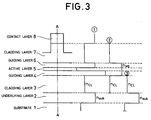
- FIG. 3 is a graph illustrating a refractive index distribution of a GaN based semiconductor laser device according to the present invention;
- FIG. 4 is a graph illustrating a relationship between a normalized frequency and an effective refractive index; and
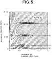
- FIG. 5 is a two-dimentional diagram illustrating how leakage light intensity varies in response to variation of a thickness of a cladding layer and an AlN molar fraction ration of the cladding of AlXGa1-XN in the GaN based semiconductor laser device according to the present invention.
-
- The GaN based semiconductor laser device according to the present invention has the same structure as that of the conventional GaN based semiconductor laser device shown in FIG. 1.
- In a refractive index distribution (1) along the line A-A in FIG. 3, nsub and nCL are taken as refractive indices of the underlying layer 2 and the n-type cladding layer 3, respectively. Further, the refractive indices of the n-type guiding layer 4, the active layer 5 and the p-type guiding layer 6 are simply averaged to yield a refractive index, nwg as the refractive index of the wave guide layer.
- In this case, two three-layer waveguide paths are defined. A first three-layer waveguide path is composed of the n-type cladding layer 3, the waveguide layer and the p-type cladding layer 7. A second three-layer waveguide path is composed of the sapphire substrate 1, the underlying layer 2, and the n-type cladding layer 3. Refractive indices of the first and second three-layer waveguide paths are given by refractive index distributions (2) and (3), respectively. See in FIG. 3.
- In the first three-layer waveguide path, a normalized frequency Vwg1 can be expressed by the following equation 1.
- As shown in FIG. 4, the normalized frequency Vwg1 calculated by Equation 1 is utilized for determining a normalized effective refractive index bwg when zero-order mode light propagates through the waveguide layer. Thus, a value 24 is determined for the first three-layer waveguide path. When the zero-order mode light, as a main lobe, is propagated through the waveguide layer having the normalized effective refractive index bwg, a high-order mode light other than the zero-order mode light, such as a first-order mode light is propagated through a mode field having a normalized frequency of a value 25. Similarly, light beams of high-order mode, for example second order or greater as side lobes, are respectively propagated through mode fields having normalized frequencies of value 26 (for second-order light beam), value 27 (for third-order light beam), value 28 (for fourth-order light beam), and value 29 (for fifth-order light beam), and so on.
- In order to prevent the leakage from the first three-layer waveguide through the n-type cladding layer 3 to the second three-layer waveguide, i.e., the underlying layer 2, the normalized frequency Vwg2 of the second three-layer waveguide path is to be selected differently from the values 25 to 29 so that the mode coupling of the second three-layer waveguide and the first three-layer waveguide path is neglected.
- The normalized frequency Vwg2 of the second three-layer waveguide path can be calculated by the following equation similarly to the case of the normalized frequency Vwg1.
- As described above, it is difficult to greatly change the refractive index of the GaN compound. Thus, if it is difficult to manufacture the underlying layer 2 so that the layer has the obtained nsub from a practical standpoint, then values of rwg or the like are differently selected in the process of calculation of Equation 1, and the calculation is repeatedly carried out to find proper solutions.
- With respect to the GaN based semiconductor laser devices composed of a waveguide layer having a thickness rwg, an underlying layer having a thickness rsub and a refractive index nsub, and an n-type cladding layer 3 having a refractive index nCL of which thickness rsub and the refractive index nsub were determined by the above calculation process, the present inventors carried out calculation by using an FEM (Finite Element Method) to plot a diagram of leakage ratio indicative of a relation between the thickness of the n-type cladding layer 3 and a molar fraction ratio x of AlN contained in the n-type AlXGa1-XN cladding layer 3. Wherein the refractive index of the n-type cladding layer 3 changes in proportion to the molar fraction ratio x of AlN contained in the n-type AlXGa1-XN cladding layer 3.
- As FIG. 5 shows, reference numeral 30 represents a region where the light leakage ratio is smaller than 10%, or where the thickness of the n-type cladding layer 3 and the molar fraction ratio x of AlN contained in the n-type cladding layer 3 constitute a favorable characteristic of the light emitting device. As will be understood from the diagram, the undesired region (i.e., a region other than the region 30) expand toward the thickness direction of the cladding layer 3 at several values 31 of the AlN molar fraction ratio. If the AlN molar fraction ratio of the AlXGa1-XN cladding layer 3 is selected to the values 31, the increase of the thickness will not contribute to suppress the leakage of the guided light. According to the GaN based semiconductor laser device of the present invention, it becomes possible to avoid an undesired AlN molar fraction ratio and corresponding refractive index from the manufacturing standpoint, with the result that it becomes possible to find a proper combination of the AlN molar fraction ratio and corresponding refractive index which satisfies the condition represented by the region 30.
- According to the GaN based semiconductor laser device of the present invention, it is possible to prevent the guided mode light generated at the active layer from leaking through the cladding layer with a small refractive index to the underlying layer. Thus, the semiconductor laser device of the present invention will exhibit an excellent light emitting characteristic.
Claims (6)
- A gallium nitride based semiconductor light emitting device having a multilayer structure obtained by depositing at least an underlying layer, an n-type cladding layer, a waveguide layer containing an active layer, and a p-type cladding layer in this order on a substrate, whereinthe n-type cladding layer, the waveguide layer and the p-type cladding layer are collectively defined as a first three-layer waveguide path and the substrate, the underlying layer and the n-type cladding layer are collectively defined as a second three-layer waveguide path, and effective refractive indices of light propagating through the first and second three-layer waveguide paths are set different from each other.
- The gallium nitride based semiconductor light emitting device according to claim 1, wherein the waveguide layer is composed of an n-type guiding layer, an active layer, and a p-type guiding layer.
- The gallium nitride based semiconductor light emitting device according to claim 1, wherein said underlying layer is GaN and has a larger refractive index than said n-type cladding layer.
- The gallium nitride based semiconductor light emitting device according to claim 1, wherein a normalized frequency of a high-order mode light corresponding to an effective refractive index of zero-order mode light determined by a normalized frequency of the first three-layer waveguide path is set different from a normalized frequency of a high-order mode light of the second three-layer waveguide path.
- The gallium nitride based semiconductor light emitting device according to claim 4, wherein the waveguide layer is composed of an n-type guiding layer, an active layer, and a p-type guiding layer.
- The gallium nitride based semiconductor light emitting device according to claim 4, wherein said underlying layer is GaN and has a larger refractive index than said n-type cladding layer.
Applications Claiming Priority (2)
| Application Number | Priority Date | Filing Date | Title |
|---|---|---|---|
| JP14161799A JP2000332361A (en) | 1999-05-21 | 1999-05-21 | Gallium-nitride-based semiconductor luminous element |
| JP14161799 | 1999-05-21 |
Publications (2)
| Publication Number | Publication Date |
|---|---|
| EP1054491A2 true EP1054491A2 (en) | 2000-11-22 |
| EP1054491A3 EP1054491A3 (en) | 2004-01-02 |
Family
ID=15296215
Family Applications (1)
| Application Number | Title | Priority Date | Filing Date |
|---|---|---|---|
| EP00110206A Withdrawn EP1054491A3 (en) | 1999-05-21 | 2000-05-17 | Gallium nitride based semiconductor light emitting device |
Country Status (3)
| Country | Link |
|---|---|
| US (1) | US6515311B1 (en) |
| EP (1) | EP1054491A3 (en) |
| JP (1) | JP2000332361A (en) |
Families Citing this family (3)
| Publication number | Priority date | Publication date | Assignee | Title |
|---|---|---|---|---|
| JP2002314203A (en) * | 2001-04-12 | 2002-10-25 | Pioneer Electronic Corp | Group iii nitride semiconductor laser and its manufacturing method |
| JP2013229638A (en) * | 2013-08-12 | 2013-11-07 | Toshiba Corp | Semiconductor light-emitting element and light-emitting device |
| CN115088149B (en) * | 2020-02-13 | 2024-12-17 | 三菱电机株式会社 | Semiconductor laser device |
Family Cites Families (1)
| Publication number | Priority date | Publication date | Assignee | Title |
|---|---|---|---|---|
| US6015979A (en) * | 1997-08-29 | 2000-01-18 | Kabushiki Kaisha Toshiba | Nitride-based semiconductor element and method for manufacturing the same |
-
1999
- 1999-05-21 JP JP14161799A patent/JP2000332361A/en active Pending
-
2000
- 2000-05-17 EP EP00110206A patent/EP1054491A3/en not_active Withdrawn
- 2000-05-22 US US09/576,859 patent/US6515311B1/en not_active Expired - Fee Related
Non-Patent Citations (4)
| Title |
|---|
| M J BERGMANN AND H C CASEY JR.: "Optical field calculations for lossy multiple-layer Al/sub x/Ga/sub 1-x/N/In/sub x/Ga/sub 1-x/N laser diodes" JOURNAL OF APPLIED PHYSICS, vol. 84, no. 3, 1 August 1998 (1998-08-01), pages 1196-1203, XP001155763 * |
| M P MACK ET AL: "Characteristics of Indium-Gallium Nitride Multiple-Quantum-Well Blue Laser Diodes Grown by MOCVD" MRS INTERNET JOURNAL OF NITRIDE SEMICONDUCTOR RESEARCH, vol. 2, 1997, XP000115596 Article 41 * |
| P G ELISEEV AND A E DRAKIN: "Analysis of the mode internal coupling in InGaAs/GaAs laser diodes" LASER PHYSICS, vol. 4, no. 3, 1994, pages 485-492, XP009019824 Interperiodica Publishing (Russia) * |
| P G ELISEEV, G A SMOLYAKOV AND M OSINSKI: "Ghost Modes and Resonant Effects in AlGaN-InGaN-GaN Lasers" IEEE JOURNAL OF SELECTED TOPICS IN QUANTUM ELECTRONICS, vol. 5, no. 3, 1999, pages 771-779, XP001155995 * |
Also Published As
| Publication number | Publication date |
|---|---|
| EP1054491A3 (en) | 2004-01-02 |
| US6515311B1 (en) | 2003-02-04 |
| JP2000332361A (en) | 2000-11-30 |
Similar Documents
| Publication | Publication Date | Title |
|---|---|---|
| JP5323087B2 (en) | Laser light source | |
| US4901123A (en) | Superluminescent diode | |
| US6593602B2 (en) | Edge emission type semiconductor device for emitting super luminescent light, its manufacture and spatial optical communication device | |
| JPH09283841A (en) | Distributed feedback semiconductor laser device, manufacturing method thereof, and exposure method | |
| US8537872B2 (en) | Light emitting device | |
| US6301283B1 (en) | Distributed feedback semiconductor laser | |
| US20140217425A1 (en) | Radiation-Emitting Semiconductor Component | |
| US8767788B2 (en) | Semiconductor laser device | |
| KR100860696B1 (en) | Vertical Resonant Surface Emission Laser | |
| US6825505B2 (en) | Phase-shifted distributed feedback type semiconductor laser diode capable of improving wavelength chirping and external reflection return light characteristics | |
| JP5069262B2 (en) | Semiconductor light emitting device and optical pulse tester using the same | |
| EP1191651A1 (en) | Distributed feedback semiconductor laser | |
| CN111129945B (en) | Method for integrally manufacturing isolator-saving edge-emitting laser chip | |
| US6515311B1 (en) | Gallium nitride based semiconductor light emitting device | |
| JP2010097032A (en) | Optical modulator | |
| JP2017139319A (en) | Semiconductor laser element | |
| US20240396306A1 (en) | Nitride semiconductor light-emitting element | |
| US20170194766A1 (en) | Optical device and optical module | |
| US20090213891A1 (en) | Semiconductor laser | |
| JPH03268379A (en) | Semiconductor laser-chip and manufacture thereof | |
| US7838444B2 (en) | Semiconductor device and fabrication method of the same | |
| JPH10150242A (en) | Grating coupled surface emitting device | |
| US6771681B2 (en) | Distributed feedback semiconductor laser | |
| JP2011192856A (en) | Semiconductor light-emitting element and optical pulse tester using the same | |
| JPH11307874A (en) | Optical isolator, distributed feedback laser and optical integrated device |
Legal Events
| Date | Code | Title | Description |
|---|---|---|---|
| PUAI | Public reference made under article 153(3) epc to a published international application that has entered the european phase |
Free format text: ORIGINAL CODE: 0009012 |
|
| AK | Designated contracting states |
Kind code of ref document: A2 Designated state(s): AT BE CH CY DE DK ES FI FR GB GR IE IT LI LU MC NL PT SE |
|
| AX | Request for extension of the european patent |
Free format text: AL;LT;LV;MK;RO;SI |
|
| PUAL | Search report despatched |
Free format text: ORIGINAL CODE: 0009013 |
|
| AK | Designated contracting states |
Kind code of ref document: A3 Designated state(s): AT BE CH CY DE DK ES FI FR GB GR IE IT LI LU MC NL PT SE |
|
| AX | Request for extension of the european patent |
Extension state: AL LT LV MK RO SI |
|
| 17P | Request for examination filed |
Effective date: 20040226 |
|
| 17Q | First examination report despatched |
Effective date: 20040413 |
|
| AKX | Designation fees paid |
Designated state(s): DE FR GB |
|
| STAA | Information on the status of an ep patent application or granted ep patent |
Free format text: STATUS: THE APPLICATION IS DEEMED TO BE WITHDRAWN |
|
| 18D | Application deemed to be withdrawn |
Effective date: 20050521 |