EP1054290A2 - Light modulator controlled by surface plasmon waves - Google Patents
Light modulator controlled by surface plasmon waves Download PDFInfo
- Publication number
- EP1054290A2 EP1054290A2 EP00304024A EP00304024A EP1054290A2 EP 1054290 A2 EP1054290 A2 EP 1054290A2 EP 00304024 A EP00304024 A EP 00304024A EP 00304024 A EP00304024 A EP 00304024A EP 1054290 A2 EP1054290 A2 EP 1054290A2
- Authority
- EP
- European Patent Office
- Prior art keywords
- light
- thin metal
- metal films
- light modulator
- mirror
- Prior art date
- Legal status (The legal status is an assumption and is not a legal conclusion. Google has not performed a legal analysis and makes no representation as to the accuracy of the status listed.)
- Granted
Links
Images







Classifications
-
- G—PHYSICS
- G02—OPTICS
- G02F—OPTICAL DEVICES OR ARRANGEMENTS FOR THE CONTROL OF LIGHT BY MODIFICATION OF THE OPTICAL PROPERTIES OF THE MEDIA OF THE ELEMENTS INVOLVED THEREIN; NON-LINEAR OPTICS; FREQUENCY-CHANGING OF LIGHT; OPTICAL LOGIC ELEMENTS; OPTICAL ANALOGUE/DIGITAL CONVERTERS
- G02F1/00—Devices or arrangements for the control of the intensity, colour, phase, polarisation or direction of light arriving from an independent light source, e.g. switching, gating or modulating; Non-linear optics
- G02F1/01—Devices or arrangements for the control of the intensity, colour, phase, polarisation or direction of light arriving from an independent light source, e.g. switching, gating or modulating; Non-linear optics for the control of the intensity, phase, polarisation or colour
- G02F1/13—Devices or arrangements for the control of the intensity, colour, phase, polarisation or direction of light arriving from an independent light source, e.g. switching, gating or modulating; Non-linear optics for the control of the intensity, phase, polarisation or colour based on liquid crystals, e.g. single liquid crystal display cells
- G02F1/133—Constructional arrangements; Operation of liquid crystal cells; Circuit arrangements
- G02F1/1333—Constructional arrangements; Manufacturing methods
- G02F1/1335—Structural association of cells with optical devices, e.g. polarisers or reflectors
- G02F1/1336—Illuminating devices
- G02F1/133621—Illuminating devices providing coloured light
-
- B—PERFORMING OPERATIONS; TRANSPORTING
- B82—NANOTECHNOLOGY
- B82Y—SPECIFIC USES OR APPLICATIONS OF NANOSTRUCTURES; MEASUREMENT OR ANALYSIS OF NANOSTRUCTURES; MANUFACTURE OR TREATMENT OF NANOSTRUCTURES
- B82Y20/00—Nanooptics, e.g. quantum optics or photonic crystals
-
- G—PHYSICS
- G02—OPTICS
- G02B—OPTICAL ELEMENTS, SYSTEMS OR APPARATUS
- G02B6/00—Light guides; Structural details of arrangements comprising light guides and other optical elements, e.g. couplings
- G02B6/10—Light guides; Structural details of arrangements comprising light guides and other optical elements, e.g. couplings of the optical waveguide type
- G02B6/12—Light guides; Structural details of arrangements comprising light guides and other optical elements, e.g. couplings of the optical waveguide type of the integrated circuit kind
- G02B6/122—Basic optical elements, e.g. light-guiding paths
- G02B6/1226—Basic optical elements, e.g. light-guiding paths involving surface plasmon interaction
-
- G—PHYSICS
- G02—OPTICS
- G02F—OPTICAL DEVICES OR ARRANGEMENTS FOR THE CONTROL OF LIGHT BY MODIFICATION OF THE OPTICAL PROPERTIES OF THE MEDIA OF THE ELEMENTS INVOLVED THEREIN; NON-LINEAR OPTICS; FREQUENCY-CHANGING OF LIGHT; OPTICAL LOGIC ELEMENTS; OPTICAL ANALOGUE/DIGITAL CONVERTERS
- G02F1/00—Devices or arrangements for the control of the intensity, colour, phase, polarisation or direction of light arriving from an independent light source, e.g. switching, gating or modulating; Non-linear optics
- G02F1/01—Devices or arrangements for the control of the intensity, colour, phase, polarisation or direction of light arriving from an independent light source, e.g. switching, gating or modulating; Non-linear optics for the control of the intensity, phase, polarisation or colour
- G02F1/19—Devices or arrangements for the control of the intensity, colour, phase, polarisation or direction of light arriving from an independent light source, e.g. switching, gating or modulating; Non-linear optics for the control of the intensity, phase, polarisation or colour based on variable-reflection or variable-refraction elements not provided for in groups G02F1/015 - G02F1/169
- G02F1/195—Devices or arrangements for the control of the intensity, colour, phase, polarisation or direction of light arriving from an independent light source, e.g. switching, gating or modulating; Non-linear optics for the control of the intensity, phase, polarisation or colour based on variable-reflection or variable-refraction elements not provided for in groups G02F1/015 - G02F1/169 by using frustrated reflection
-
- G—PHYSICS
- G02—OPTICS
- G02F—OPTICAL DEVICES OR ARRANGEMENTS FOR THE CONTROL OF LIGHT BY MODIFICATION OF THE OPTICAL PROPERTIES OF THE MEDIA OF THE ELEMENTS INVOLVED THEREIN; NON-LINEAR OPTICS; FREQUENCY-CHANGING OF LIGHT; OPTICAL LOGIC ELEMENTS; OPTICAL ANALOGUE/DIGITAL CONVERTERS
- G02F1/00—Devices or arrangements for the control of the intensity, colour, phase, polarisation or direction of light arriving from an independent light source, e.g. switching, gating or modulating; Non-linear optics
- G02F1/01—Devices or arrangements for the control of the intensity, colour, phase, polarisation or direction of light arriving from an independent light source, e.g. switching, gating or modulating; Non-linear optics for the control of the intensity, phase, polarisation or colour
- G02F1/23—Devices or arrangements for the control of the intensity, colour, phase, polarisation or direction of light arriving from an independent light source, e.g. switching, gating or modulating; Non-linear optics for the control of the intensity, phase, polarisation or colour for the control of the colour
-
- G—PHYSICS
- G02—OPTICS
- G02F—OPTICAL DEVICES OR ARRANGEMENTS FOR THE CONTROL OF LIGHT BY MODIFICATION OF THE OPTICAL PROPERTIES OF THE MEDIA OF THE ELEMENTS INVOLVED THEREIN; NON-LINEAR OPTICS; FREQUENCY-CHANGING OF LIGHT; OPTICAL LOGIC ELEMENTS; OPTICAL ANALOGUE/DIGITAL CONVERTERS
- G02F1/00—Devices or arrangements for the control of the intensity, colour, phase, polarisation or direction of light arriving from an independent light source, e.g. switching, gating or modulating; Non-linear optics
- G02F1/01—Devices or arrangements for the control of the intensity, colour, phase, polarisation or direction of light arriving from an independent light source, e.g. switching, gating or modulating; Non-linear optics for the control of the intensity, phase, polarisation or colour
- G02F1/13—Devices or arrangements for the control of the intensity, colour, phase, polarisation or direction of light arriving from an independent light source, e.g. switching, gating or modulating; Non-linear optics for the control of the intensity, phase, polarisation or colour based on liquid crystals, e.g. single liquid crystal display cells
- G02F1/133—Constructional arrangements; Operation of liquid crystal cells; Circuit arrangements
- G02F1/1333—Constructional arrangements; Manufacturing methods
- G02F1/133394—Piezoelectric elements associated with the cells
-
- G—PHYSICS
- G02—OPTICS
- G02F—OPTICAL DEVICES OR ARRANGEMENTS FOR THE CONTROL OF LIGHT BY MODIFICATION OF THE OPTICAL PROPERTIES OF THE MEDIA OF THE ELEMENTS INVOLVED THEREIN; NON-LINEAR OPTICS; FREQUENCY-CHANGING OF LIGHT; OPTICAL LOGIC ELEMENTS; OPTICAL ANALOGUE/DIGITAL CONVERTERS
- G02F1/00—Devices or arrangements for the control of the intensity, colour, phase, polarisation or direction of light arriving from an independent light source, e.g. switching, gating or modulating; Non-linear optics
- G02F1/01—Devices or arrangements for the control of the intensity, colour, phase, polarisation or direction of light arriving from an independent light source, e.g. switching, gating or modulating; Non-linear optics for the control of the intensity, phase, polarisation or colour
- G02F1/13—Devices or arrangements for the control of the intensity, colour, phase, polarisation or direction of light arriving from an independent light source, e.g. switching, gating or modulating; Non-linear optics for the control of the intensity, phase, polarisation or colour based on liquid crystals, e.g. single liquid crystal display cells
- G02F1/133—Constructional arrangements; Operation of liquid crystal cells; Circuit arrangements
- G02F1/1333—Constructional arrangements; Manufacturing methods
- G02F1/1335—Structural association of cells with optical devices, e.g. polarisers or reflectors
- G02F1/1336—Illuminating devices
- G02F1/133621—Illuminating devices providing coloured light
- G02F1/133622—Colour sequential illumination
-
- G—PHYSICS
- G02—OPTICS
- G02F—OPTICAL DEVICES OR ARRANGEMENTS FOR THE CONTROL OF LIGHT BY MODIFICATION OF THE OPTICAL PROPERTIES OF THE MEDIA OF THE ELEMENTS INVOLVED THEREIN; NON-LINEAR OPTICS; FREQUENCY-CHANGING OF LIGHT; OPTICAL LOGIC ELEMENTS; OPTICAL ANALOGUE/DIGITAL CONVERTERS
- G02F2203/00—Function characteristic
- G02F2203/10—Function characteristic plasmon
Definitions
- the present invention relates to a light modulator.
- a light modulator utilizing surface plasmon, a light source and a display apparatus using the light modulator, and a method for driving the light modulator will be described below, by way of example in illustration of the invention.
- a field sequential display apparatus using a colour filter disk has previously been proposed in a publication entitled "Colour Liquid Crystal Display” written and edited by Shunsuke Kobayashi and published on Dec. 14, 1990, at page 117.
- a colour filter disc coloured in red, green, and blue i.e., the three primary colours of light
- a colour display is also made possible by placing the colour filter disc in front of a white light source, combined with a black-and-white shutter type display device.
- a light modulator utilizing an electromagnetic wave supported by the interface between a metal and an insulator (a dielectric material), referred to as a surface plasmon wave (SPW) device, a display apparatus which permits colour display by utilizing this light modulator, and a light source thereof as a display apparatus, whereby a colour display is implemented without using the foregoing colour filter and colour light source.
- SPW surface plasmon wave
- Conductors such as metals, which can be defined as a gas of electrons in electrostatic equilibrium inside a continuum of positive fixed charges, can be considered as a "condensed" electron plasma with an electron density approximately equal to 10 23 electrons per cm 3 , in which a longitudinal wave, referred to as a surface plasma oscillation, is able to exist in addition to a volume plasma oscillation, which is a normal plasma oscillation.
- the electric field due to the surface plasma oscillation has a periodic wave form in a direction parallel to the metal surface, while having the form of an evanescent wave which evanesces exponentially in a direction perpendicular to the metal surface.
- Plasmons are quanta associated with the plasma oscillation (collective wave excitation of a conductive electronic gas) in the metal. Because of the high electron density, quantum effects dominate.
- the surface plasmon waves can be optically excited by resonant coupling. The condition for resonance is strongly dependent on the refractive indices and thickness of the media near to the metal-insulator interface.
- the intensity of the light wave can be modulated by coupling the light wave with the surface plasmon wave. Generally, if coupling between the surface plasmon wave and the light wave is strong, the attenuation of the emitted light wave is strong, and, if coupling is weak, there occurs almost no attenuation of the emitted light wave.
- Attenuated total reflection (ATR) effect has been utilized to optically excite surface plasmon waves through a high-index prism.
- Light traveling in free-space, is sent towards the metal-insulator interface through the prism with an angle larger than the critical angle, producing an evanescent wave field which may overlap the surface plasmon wave field.
- Kev of the evanescent wave is in harmony with the propagation constant Ksp of the surface plasmon, the surface plasmon resonance is excited on the metal surface.
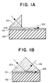
- Two configurations are mainly used for optically exciting the surface plasmon wave. The first is Otto's ATR configuration. This Otto's configuration is shown in Fig. 1A.
- c the speed of light in vacuum
- ⁇ the angular frequency
- ⁇ the wavelength
- n( ⁇ ) and n( ⁇ ) are the refractive indices of the prism in the case of an angular frequency ⁇ and a wavelength ⁇
- K 0 ( ⁇ ) is the wave number in the case of an angular frequency ⁇ in vacuum
- ⁇ is the incident angle of light with respect to the underside of the prism. Therefore, the wave number of the evanescent waves can be harmonized with the propagation constant of the metal surface plasmon by adjusting the refractive index n( ⁇ ) or
- the propagation constant Ksp is also a complex number.
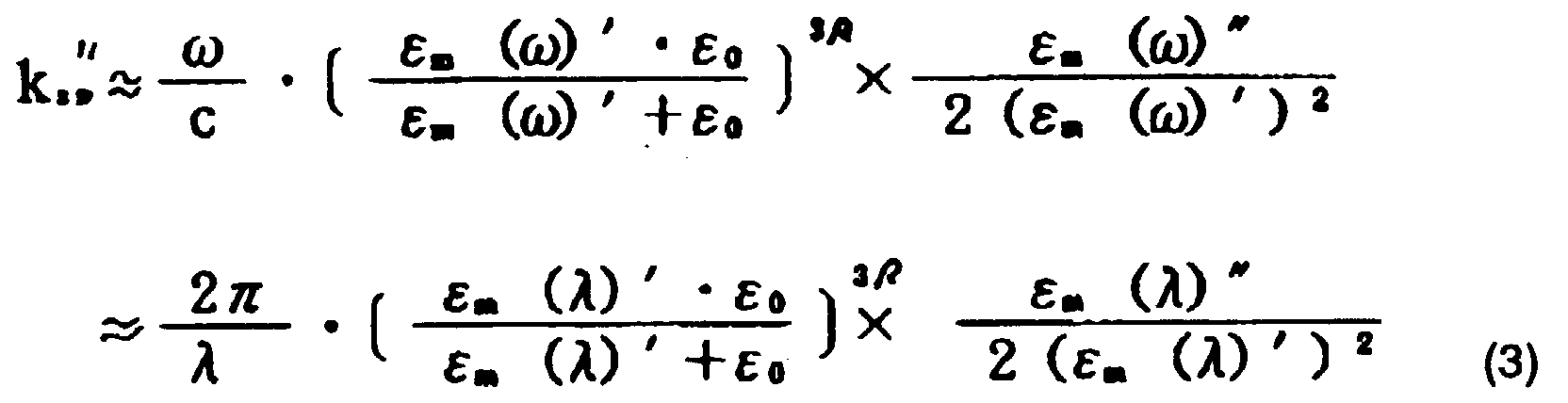
- the metal surface plasmon itself must be a wave with a long life. That is, it is required that the imaginary part of the propagation constant Ksp is small, and the attenuation associated with propagation is small.
- the factor which decides the intensity of the metal surface plasmon is ⁇ m'' / ( ⁇ m') 2 ( ⁇ , to be precise, depends on the angular frequency or the wavelength), and the metal to excite the metal surface plasmon is desirably a metal whose value of
- silver (Ag), gold (Au), copper (Cu), aluminum (Al) and the like are usable.
- FIG. 2A there is illustrated a device whereby the absorption wavelength is made variable, and the wavelength region of the reflected light is electrically changed using a liquid crystal.
- Fig. 2B shows the measurements (a broken curve) and the calculated results (solid curve) of the characteristics of the reflected light intensity with respect to wavelengths when the voltage value in the aforesaid device is varied.
- a 60° SF 6 glass prism is used as a prism 103, and a 50-nm silver thin film is evaporated thereon as a thin metal film 101.
- a 50-nm MgF 2 layer is then evaporated at a 50° oblique angle on to the silver film as an alignment layer 108.
- a substrate 110 is so configured that the same alignment layer 108 is obliquely evaporated on to an ITO film, which is a transparent electrode formed on a glass substrate.
- a 4- ⁇ m cell gap is ensured by spacers 109, and then filled with BL009 manufactured by Merck KGaA as a liquid crystal 107.
- a white light is incident on the device through a sheet polarizer as a p- and linearly polarized light, and a voltage is applied thereto to determine the dependence of the reflected light on the wavelength.
- the results are shown in Fig. 2B.
- At a voltage of 0 V there is an absorption maximum in the vicinity of 640 nm. The absorption maximum shifts towards the lower wavelengths with the application of a voltage.
- 10V it is at 560 nm, and at 30 V, it is at 450 nm.
- the measured results are in good agreement with the calculated results.
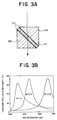
- Fig. 3A is a cross sectional view of a device for obtaining transmitted light in a specific wavelength range by implementing the Kretschmann method in a symmetrical structure.
- Fig. 3B is a diagram showing the calculated results of the transmitted light intensity with respect to the wavelength when the refractive index of the central medium is changed in the device.
- This device is considered in the same way as the one obtained by removing the substrate 110 side, and providing a structure identical with the upper side structure on the lower side in symmetrical relation to the device having the structure shown in Fig. 2A.
- the film thickness of the electro-optical material 111 of the central part is much thinner compared to that of the device of Fig. 2A.
- This symmetrical structure and the very thin central electro-optical material 111 enable the surface plasmon wave generated at the interface on the incident side to be coupled to the surface plasmon wave at the next interface with the metal to generate another surface plasmon wave on the outgoing side.
- This surface plasmon wave re-radiates the light with the same wavelength. In this manner, it is possible to re-radiate the absorbed light.
- 3B shows theoretical calculated results when the anisotropic refractive index dn of the central material is changed from 0 to 0.2, and 0.5 in this device.
- the device radiates light at a wavelength of 450 nm.
- dn at 0.2 and 0.5, light at respective wavelengths of 530-nm and 650-nm are radiated.
- surface plasmon is a surface effect, the film thickness of the central material is arranged to be very thin, or about one wavelength in order to effect such re-radiation.
- the response speed can be about two orders of magnitude faster than the response speed of a conventional liquid crystal device, because of the thinness of the film.
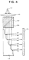
- FIG. 4 shows an example of the configuration of a direct-view type liquid crystal display apparatus for performing a field sequential display utilizing surface plasmon.
- one device of Fig. 3A is used as a device 100.
- the light from a line source 112 is incident through a cylindrical lens 113 on to the device 100, and one colour of the three primary colours of light is selected for each time period.
- the light is applied on to the whole surface of a liquid crystal panel 115 by a reflector 114 having a stepped surface to permit field sequential display.
- a reflector 114 having a stepped surface to permit field sequential display.
- 5,570,139 provides an example of a light source for a liquid crystal display device using a surface plasmon and will be described with reference to Fig. 5.
- White light is applied from the upper right to be sequentially incident on a plurality of (three) unit devices 100A, 100B, and 100C.
- the outgoing light therefrom establishes itself as a light source.
- light beams of specific wavelength ranges i.e., blue, green, and red light beams are individually absorbed to obtain respective colours of yellow, magenta, and cyan. This cycle is repeated in the three devices to obtain a light of a prescribed colour.
- FIG. 6 is a cross sectional view of an example of the projector utilizing surface plasmon according to this technique.
- a central surface plasmon device 100D has almost the same structure as the one shown in Fig. 5, except that the prisms 103 of Fig. 5 are integrated into one unit.
- a reflection type liquid crystal display apparatus or the like which performs monochrome modulation through a projection lens 121 to obtain an image on the outgoing side, thus providing an image display.
- the light from the lamp is collected in one direction by the reflector, and then brought close to a parallel beam in a narrow region by the relay lens and the integrator.
- the light beam is then aligned into either polarized light by the sheet polarizer, and the selection of colour and image display are carried out at the surface plasmon device.
- the image is projected through the projection lens.
- the projection can be accomplished based on a field sequential display.
- a light modulator in which a metal-insulator interface is formed adjacent to a planar wave guide for carrying a light wave.
- a high frequency voltage applied to the interface causes the insulator to resonate, generating a surface plasmon wave on the interface.
- the resulting wave is coupled to a gradually vanishing light wave in the wave guide, thus changing the intensity of the light wave.
- the foregoing light modulators especially, the light modulator using surface plasmon, and a display apparatus using the same, encounter the following problems.
- the first problem lies in that the structure is complicated. This is attributable to the fact that, in the previous proposals, three unit devices each having a wavelength variable by an electric field are required for simultaneously obtaining light beams of the three primary colours in specific wavelength ranges.
- the second problem lies in that the loss of light is high. The reason for this is that there is used only the reflected light from which light has been absorbed by the surface plasmon, or the re-radiated light of the absorbed light. Therefore, the whole of the light is not used which results in a loss. For example, with the technique of Fig. 4, during the period in which one colour produced by the field sequential display is displayed, the other two colours of the three primary colours are not used at all.
- the third problem lies in that there exists no light modulator capable of ensuring a division both temporally and spatially.
- the present invention relates to a light modulator utilizing surface plasmon generated at the interface between a thin metal film and an electro-optical material.
- a particular arrangement to be described in illustration of the present invention has two unit devices, and a mirror, the two unit devices, each having a pair of prisms individually provided with thin metal films at their respective undersides, in which the thin metal films are oppositely disposed, and an electro-optical material sandwiched between the oppositely disposed thin metal films, in which the two unit devices are disposed in parallel to each other such that respective surfaces of the prisms of the unit devices are in contact with each other so as to ensure the arrangement of the thin metal films in a parallel relation to each other, and the mirror is disposed such that the mirror side thereof faces a direction in parallel with the thin metal films, and extends along the top of the prism of one unit device on the side thereof not in contact with another unit device.
- a liquid crystal material is used in the particular arrangement.
- an air gap can be employed in place of the electro-optical material.
- the thickness of the air gap may also be changed by a piezo material provided between the prisms constituting the unit device.
- the maximum amount of the incident light can be utilized in the final outgoing light with a minimum of loss by making both of the transmitted light due to absorption and re-radiation generated by the unit device and the reflected light into the outgoing light, the light incident on the next unit device, or the light incident on the mirror.
- the colour of light can be spatially divided. Still further, it can also be divided temporally by changing the wavelength by means of a voltage.
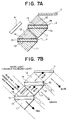
- the apparatus of the first configuration includes first and second unit devices 1 and 2 each implementing the Kretschmann method in a symmetrical structure, and one mirror 3. If required, a device for aligning the polarization direction in one direction may be added. Here, a polarization conversion device 4 is provided in a light incident path.
- the first and second unit devices 1 and 2 each implementing the Kretschmann method in a symmetrical structure are so configured that the respective inclined surfaces of two prisms 11 and 12, each having a right triangle cross section, are oppositely disposed, and thin metal films 13 and 14 are respectively formed on the inclined surfaces. Further an electro-optical material 15 whose refractive index varies in accordance with the electric field strength is inserted between the oppositely disposed thin metal films 13 and 14.
- the first and second unit devices 1 and 2 are arranged in a parallel relation to each other with a respective surface of each of the prisms substantially in contact with each other.
- each underside of the prisms 11 and 12 and the thin metal films 13 and 14 are arranged in a parallel relation to one another.
- the surface side of the mirror 3 is also disposed so that it is parallel to the aforesaid parallel plane, and one end thereof is substantially in contact with the top of the prism of the second unit device 2 on the side thereof not in contact with the first unit device 1.
- the polarization conversion device 4 is disposed at the incident light side position of the first unit device 1 not in contact with the mirror 3, i.e., at a position opposing the side of the prism 12 not in contact with the second unit device 2.
- FIG. 7B is a diagram suitable for use in illustrating the operation of the apparatus of the first configuration. It is a diagram schematically showing how the light beams of three primary colours of R, G, and B (red, green, and blue) are transmitted.
- the white light which has been converted into linearly polarized light by the polarization conversion device 4 is incident on one surface of the prism 12 of the first unit device 1, and reaches the thin metal film 14.
- the first unit device 1 on the incident side absorbs red light, and re-radiates it. Therefore, red light is emitted.
- the reflected light including the other green and blue light is incident on the second unit device 2.
- the light reaches the thin metal film 13 through the prism 11, and blue light is absorbed, and re-radiated. Therefore, green light is emitted as reflected light. Further, blue light passes through the second unit device 2, and then it is reflected by the mirror 3, and emitted therefrom. Thus, white light is spatially divided in the order of red, green, and blue. Further, the refractive index of the electro- optical material 15 is changed by individually applying to the first unit device 3 and the second unit device 2 a voltage. Therefore it is possible to change the wavelength of the light to be absorbed and re-radiated.
- the white light is spatially divided in the order of green, blue, and red.
- the spatially divided light can also be divided temporally by performing temporal switching in this manner.
- the loss of light is also very low.
- the polarization conversion device 4 for aligning non-polarized light with linearly polarized light on the incident side there is almost no loss of light.
- a liquid crystal material is used as the electro-optical material 15 whose refractive index varies with the electric field of the arrangement of the first configuration.
- an alignment layer is formed for aligning the liquid crystal material, as required.
- the operation of the second configuration is similar to that of the first configuration.
- the liquid crystal alignment of the liquid crystal material serving as the electro-optical material 15 is changed by the application of a voltage, and the refractive index of the liquid crystal material changes due to the anisotropic refractive index which the liquid crystal has. Consequently, it is possible to change the wavelength by means of a voltage. Especially noteworthy is the following fact.
- the liquid crystal material region is a very thin film with a thickness of about one wavelength, switching is done based not on the bulk of the material, but based on only the surface of the material. Accordingly, a response can be obtained which is about two orders of magnitude faster than by using the usually employed liquid crystal material. Consequently, a light modulator capable of giving a comparatively fast response can be obtained.
- prisms of 60° SF 6 glass are used as the prisms 11 and 12 of the first and second unit devices 1 and 2, and silver thin films are evaporated thereon as the thin metal films 13 and 14. Further, MgF 2 is obliquely evaporated thereon as an alignment layer, which is not shown. A liquid crystal is sandwiched as the electro-optical material 15 between the prisms 11 and 12. Thus, the prisms 11 and 12 are joined together without using an adhesive.
- the thin metal films 13 and 14 are wired so as to enable a voltage to be applied to them.
- the first and second unit devices 1 and 2 are each thus configured and are optically cemented to each other using a matching oil with a refractive index of 1.805, almost the same as that of SF 6 . Further, a mirror 3 is included.
- the light from a white light source is shone thereon through a sheet polarizer serving as the polarization conversion device 4.
- the light is then spatially divided into red, green, and blue by applying a voltage via the wiring, i.e., between the thin metal films 13 and 14. Further, it is possible to achieve temporal switching by adjusting the voltage value. It is also possible to provide high-speed switching in the order of (1) red, green, and blue, (2) green, blue, and red, and (3) blue, red, and green.
- one of the prisms 11 or 12 at least has a rutile crystal structure obtained by heating titanium oxide.
- the refractive index is about 2.8.
- the first and second unit devices 1 and 2 are made using the prisms, and are arranged in a parallel relation to each other, and the mirror 3 is included.
- the efficiency is enhanced by the effects of the polarization conversion device and the use of the high refractive index prisms much more than with the previously described configuration.
- the efficiency using the rutile prism was found to be higher.
- FIG. 8A is a diagram showing the configuration of the third configuration. Piezo materials 16 are disposed respectively on both ends of the space between the prisms 11 and 12 in place of the electro-optical material 15 provided in the first configuration, and thus, there is an air gap 17 between the prisms 11 and 12 provided by the piezo materials 16.
- FIGS. 8B and 8C are diagrams for use in describing the operation of the third configuration, in which, as distinct from the first and second configurations, the application of a voltage changes not the refractive index, but the thickness of the air gap 17.
- the application to the piezo materials 16 of a voltage causes distortion according to the voltage value.
- elongation, as shown FIG. 8B, or shrinkage, as shown in FIG. 8C occurs, thereby making it possible to change the thickness of the air gap 17.
- the coupling conditions for the surface plasmon are changed by utilizing this property to obtain the same effects as in the first and second configurations.
- the advantage of this method is that, since the region of the air gap 17 has a lower refractive index than a liquid crystal as compared with the case where the liquid crystal is used, the prisms 11 and 12 are not required to have high refractive indices. This is advantageous in achieving a lower cost.
- a specific example of the third configuration includes the use of zinc oxide (ZnO) which enables a thinner film for the material having the piezoelectric effect to be achieved more easily.
- the device of this arrangement can be manufactured in the same manner. as in the second configuration, except that a liquid crystal is not used, and the following process is employed for using the piezo material.
- Thin films 16 of zinc oxide are formed and patterned on both ends of the silver thin film 13 on each prism 11 of the unit devices 1 and 2. Then, a silver paste is applied thereon in a very small amount by means of a control type dispenser to be joined together with the side of the prism 12 on which the silver thin film 14 is formed.
- the air gap 17 is formed between respective silver thin films 13 and 14 of the prisms 11 and 12 by the zinc oxide thin film 16.
- the mirror 3 and the polarization conversion device 4 are used.
- This specific example can provide the same high efficiency as in the specific example of the first configuration.
- zinc oxide is used as the piezo material, but any material can be employed as long as they can be formed into sufficiently thin films.
- AIN aluminum nitride
- a good thin film can be formed by means of a magnetron sputtering method or a dual beam sputtering method.
- zinc oxide a better thin film can be obtained by means of an ECR plasma sputtering method.
- a comparatively thin film can also be achieved with a PZT system.
- the material exhibiting a piezoelectric effect in the same manner as in the third configuration.
- an air gap 17 is provided in place of the electro-optical material 15 in the first configuration.
- Materials 16 exhibiting a piezoelectric effect are respectively placed on the surfaces of the respective prisms 11 and 12 of the unit devices 1 and 2 through which light of incidence, transmission, reflection, or the like will not pass.
- the thickness of the air gap is varied in the same manner as in the third configuration.
- the application to the piezo materials 16 of a voltage causes distortion according to the value of a voltage. As a result, elongation, as shown FIG.
- the piezo material 16 is not required to be formed into a thin film, and when disposed on the whole surface of each prism as shown in FIGS. 9A, 9B, and 9C, patterning accuracy is not required, because patterning is not necessary, resulting in a lower manufacturing cost. Further, the electrode for the piezo material 16 is easy to extract.
- diffraction gratings are used in place of the prisms 11 and 12 of the first to the fourth configurations.
- a diffraction grating 18 is used at each portion on which the prism of the first configuration was placed. That is, thin metal films 13 and 14 are respectively formed on both surfaces of the electro-optical material 15, with a desired thickness.
- the diffraction gratings 18 are individually disposed on their respective surfaces of the thin metal films 13 and 14. For the diffraction grating 18, a diffraction grating having a shorter period than the wavelength of the incident light is selected.
- either the electro-optical material such as a liquid crystal, or a material exhibiting a piezoelectric effect may be used.
- the same operation as in the first configuration is possible.
- a particularly large prism is not required. As a result, the whole apparatus becomes compact in size, and there is a reduction in weight.
- FIG. 11 shows the configuration adapted to the first configuration as the sixth configuration.
- a filter 19 for improving the wavelength characteristics is arranged at the outgoing side of the second unit device 2.
- the filter 19 has characteristics that compensate for differences in wavelength range and intensity between the outgoing light which has been absorbed and re-radiated at each unit device and the outgoing light which has undergone only absorption, and has been reflected at the unit device 1 and the unit device 2.
- the characteristics of the filter 19 are, if required, also the characteristics for cutting the wavelength region wherein absorption will not arise satisfactorily from the surface plasmon absorption under the conditions such as the voltage, film thickness, and refractive index to be used.
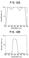
- FIG. 12A shows one example of the characteristics of the filter used in this sixth embodiment.
- the characteristics are of the absorption and re-radiation close to the characteristics shown in FIG. 8B. It is indicated that the characteristics are for cutting the light within the unnecessary wavelength region included in the light reflected from the second unit device when the light modulator has peaks at wavelengths of 460 nm, 550 nm, and 680 nm.
- FIG. 12B shows the wavelength characteristics of the outgoing light in each unit space spatially divided when the sixth configuration is implemented. It shows the case where red light and blue light is absorbed and re-radiated at the first unit device 1 and the second unit device 2, respectively, and green light is reflected from the second unit device 2. It is indicated that the unnecessary wavelength region is cut so that the spatial division of colours is satisfactorily achieved.
- the seventh configuration relates to a method for applying an electric field, i.e., a driving method for use in the first to the sixth configurations.
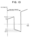
- FIG. 13 shows one example of the driving method in the seventh configuration.
- This example of the driving method includes the feature that it does not set as a constant the wavelength of the light absorbed within the field sequential sub-field time, but shifts it, as shown in the Figure. That is, the amplitude of the voltage to be applied within the sub-field is changed.
- FIG. 14A is a graph showing the wavelength characteristic range to be shifted by the driving method.
- FIG. 14 B is a graph showing the difference in wavelength characteristics between the case in which the driving method is utilized (solid curve) and the case in which it is not used (a broken curve).
- the driving method of this seventh configuration since the amplitude of the voltage to be applied within the sub-field time is varied, the emitted light corresponds to the time average of the one which has shifted its wavelength characteristics in accordance with the change. Therefore, it is possible to adjust the width of the wavelength region. At the same time, the wavelength region of the light reflected from the second unit device can also be adjusted.
- FIG. 14B although a positive and a negative symmetrical voltage are to be applied on the liquid crystal portion, the application of a voltage of only either polarity is sufficient, whereby problems, such as image persistence, will not occur. Even in the case of the piezo material, the conditions for the applied voltage value differs therefrom, but the implementation is possible in the similar manner.
- a compression colour division light source is configured by using one light modulator of the first to the seventh configurations.
- the compression colour division light source denotes a source of both temporally and spatially divided light, and having a low loss of light.
- the arrangement can be implemented by a combination of a white light source including light beams covering a large number of wavelength regions, or the like, and the light modulator of the first configuration.
- the arrangement can be implemented by a combination of the white light source, or the like, and any one light modulator of the second to the seventh configurations.
- the light source of this eighth configuration minimises any loss of light in the field sequential display.
- a liquid crystal display apparatus of the field sequential method is configured by using any one light modulator of the first to the seventh configurations, or the compression colour division light source of the eighth configuration.
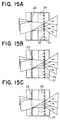
- FIGS. 15A to 15C are views illustrating a part of the liquid crystal display apparatus of the ninth configuration, and the operation thereof. That is, a liquid crystal 20 of the liquid crystal display apparatus is configured as a liquid crystal panel of the direct-view type, the reflection type, or the projection type.
- One micro lens 23 is disposed opposite to every set of three aperture portions 22 out of the aperture portions individually defined by the respective light-shielding portions 21 of the liquid crystal 20.
- any one light modulator or light source of the first to the eighth configurations is placed at the left-hand side outside the Figure with respect to each micro lens 23.
- the optical path of light of each divided colour is adjusted by the lens, and the light is to be incident from the left hand side of the Figure.
- the light enters the liquid crystal layer through each micro lens, and passes through a picture element structure from the aperture portions and the light shielding portions.
- red, blue, and green light are sequentially displayed on their respective pixels, vertically from the highest one.
- green, red, and blue are displayed in this order, as shown in FIG. 15B, and in the final period, blue, green, and red are displayed in this order as shown in FIG. 15C.
- Repetition of this procedure permits the field sequential display by a method whereby colours are switched individually on each picture element. Consequently, a liquid crystal display apparatus with a relatively low loss of light can be obtained.
- a projector is configured on the basis of the first to the ninth configurations.
- this tenth configuration is implemented by adapting the first to the ninth configurations to a part of the projector apparatus. The operation thereof similar to that described above.
- the projection type such as the use of a projector shows a high loss of light, and hence requires a high intensity of the light from the source.
- this arrangement has presented problems due to an increase in dissipation power, a reduction in the size of the apparatus, and the like. With the configuration of this arrangement, a projector with a minimum loss of light can be obtained.
- a display method with a projector there are methods using other various apparatuses such as a DMD (digital mirror device) and a TMA (thin film micro-mirror array), other than the method using the liquid crystal display apparatus of the particular ninth configuration described. Further, an arrangement using a large number of these devices is also possible.
- DMD digital mirror device
- TMA thin film micro-mirror array
- the eleventh configuration illustrative of the present invention relates to a method for driving the liquid crystal display apparatus used in the ninth configuration, or the projector used in the tenth configuration.
- the light beams which have been spatially divided and emitted, have different intensities for every unit space. This is attributable to the design and manufacturing conditions of the unit device, differences in the reflectance of the mirror, and the optical path difference, and the medium for the optical path, and the like, other than the difference in intensity between the light emitted due to the absorption and re-radiation, and the light emitted due to only double absorption and reflection.
- the liquid crystal display apparatus or the projector is driven so as to correct the differences by an apparatus for monochrome modulation, or the like to be used therein.
- FIGS. 16A and 16B are graphs for use in describing the operation of the eleventh configuration.
- FIG. 16A shows the intensity of each spatially divided light beam obtained by the light modulator.
- FIG. 16B shows the range in which the intensity of the monochrome modulation for the characteristics of FIG. 16A is set.
- the result of the synergistic effect between the characteristics of FIGS. 16A and 16B can be obtained as an actual display. This method can minimise the difference in intensity generated by the light modulator.
- the light modulator has two unit devices utilizing the surface plasmon generated at the interface between a thin metal film and an electro-optical material, and a mirror. Both the transmitted light due to absorption and re-radiation, and the reflected light generated by the unit device are outgoing light, incident light on the next unit device, or incident light on the mirror. Consequently, all light beams can be utilized as the final outgoing light beams with no loss of light. Further, the colour of the light can be spatially divided, and still further, it can also be temporally divided by changing the wavelength by means of a voltage.
- the structure is very simple.
- the transmitted light which has been re-coupled by a symmetrical structure and the reflected light are used carefully and effectively, the light can be utilized effectively with a very low loss of light.
- the light can be spatially divided into respective wavelength regions by means of the device structure, while it can also be temporally divided as a result of the variance of the wavelength due to the application of an electric field, there can be provided a light modulator capable of performing a division both temporally and spatially.
- the apparatus can be implemented at a comparatively low cost.
- a diffraction grating may be used in place of the prisms, the whole apparatus may be compact in size, and of a reduced weight.
- a filter for correcting the wavelength characteristics is used, and the wavelength characteristics are improved by means of the particular driving method, the wavelength characteristics of the emitted light are enhanced.
Landscapes
- Physics & Mathematics (AREA)
- Nonlinear Science (AREA)
- Optics & Photonics (AREA)
- General Physics & Mathematics (AREA)
- Engineering & Computer Science (AREA)
- Chemical & Material Sciences (AREA)
- Nanotechnology (AREA)
- Crystallography & Structural Chemistry (AREA)
- Life Sciences & Earth Sciences (AREA)
- Biophysics (AREA)
- Microelectronics & Electronic Packaging (AREA)
- Mathematical Physics (AREA)
- Liquid Crystal (AREA)
- Optical Modulation, Optical Deflection, Nonlinear Optics, Optical Demodulation, Optical Logic Elements (AREA)
- Electrochromic Elements, Electrophoresis, Or Variable Reflection Or Absorption Elements (AREA)
Abstract
Description
Claims (11)
- A light modulator using surface plasmon waves generated at the interface between a thin metal film and an electro-optical material, including two unit devices (1,2) and a mirror (3), the two unit devices (1,2), each having a pair of prisms (11,12) individually provided with thin metal films (13,14) on their respective undersides, the thin metal films being oppositely disposed, and an electro-optical material (15) sandwiched between the oppositely disposed thin metal films, and the two unit devices being disposed in parallel to each other such that respective ones of the surfaces of the prisms of the unit devices are in contact with each other so as to ensure the arrangement of the thin metal films in a parallel relation to each other, and the mirror being disposed such that the mirror faces in a direction parallel to the thin metal films, and extends along the top of the prism of one unit device on the side thereof not in contact with another unit device.
- A light modulator as claimed in claim 1, in which liquid crystal material is used as the electro-optical material (15).
- A light modulator using surface plasmon waves generated at the interface between a thin metal film and an electro-optical material, including, two unit devices (1,2) and a mirror (3), in which the two unit devices (1,2), each have a pair of prisms (11,12) individually provided with thin metal films (13,14) on their respective undersides, and the thin metal films are oppositely disposed with an air gap in between, and a piezo material (16) is sandwiched between the thin metal films so as to ensure the air gap, the two unit devices being disposed in parallel to each other such that a respective surface of one of the prisms of each of the unit devices is in contact with that of another so as to ensure the arrangement of the thin metal films in a parallel relation to each other, and the mirror being disposed such that the side of the mirror faces the direction in parallel to the thin metal films, and extends along the top of the prism of one unit device on the side thereof not in contact with another unit device.
- A light modulator using surface plasmon waves generated at the interface between a thin metal film and an electro-optical material, including two unit devices (1,2) and a mirror (3), in which two unit devices (1,2), each have a pair of prisms (11,12) individually provided with thin metal films (13,14) at their respective undersides, the thin metal films being oppositely disposed with an air gap in between, and a piezo material (16) being disposed on one surface of the prism through which the light to be modulated will not pass, and the two unit devices being disposed in parallel to each other such that respective ones of the surfaces of the prisms of the unit devices are in contact with each other so as to ensure the arrangement of the thin metal films in a parallel relation to each other, the mirror being disposed such that the mirror side thereof faces the direction in parallel to the thin metal films, and extends along the top of the prism of one unit device on the side thereof not in contact with another unit device.
- A light modulator as claimed in any one of claims 1 to 4, including a diffraction grating (18) in place of a prism.
- A light modulator as claimed in any one of claims 1 to 5, including a device for aligning the polarization direction into one direction, the device being disposed on the incident light side of the other unit device not in contact with the mirror.
- A light modulator as claimed in any one of claims 1 to 6, including a filter for adjusting the wavelength characteristics disposed on the outgoing side of the one unit device.
- A method for driving a light modulator as claimed in any one of claims 1 to 7, including the steps of spatially dividing the incident light into light beams of a plurality of wavelengths, and changing the voltage to be applied to the thin metal films.
- A light source of a compression colour division system, including a combination of the light modulator as claimed in any one of claims 1 to 7 and a source of white light to be incident on the light modulator.
- A display apparatus including an illumination unit using the light modulator as claimed in any one of claims 1 to 7, or the light source as claimed in claim 9, which illuminates a liquid crystal panel, and a display unit to display a projected image on the liquid crystal panel or a screen.
- A method for driving a display apparatus as claimed in claim 10, including the step of driving the display apparatus so as to correct a difference in intensity of optical power on spatial division due to the light modulator.
Priority Applications (1)
| Application Number | Priority Date | Filing Date | Title |
|---|---|---|---|
| EP04016812A EP1473586B1 (en) | 1999-05-14 | 2000-05-12 | Light modulator controlled by surface plasmon waves |
Applications Claiming Priority (2)
| Application Number | Priority Date | Filing Date | Title |
|---|---|---|---|
| JP13358599A JP3402253B2 (en) | 1999-05-14 | 1999-05-14 | Light modulation element, light source and display device using the same, and method of driving the same |
| JP13358599 | 1999-05-14 |
Related Child Applications (1)
| Application Number | Title | Priority Date | Filing Date |
|---|---|---|---|
| EP04016812A Division EP1473586B1 (en) | 1999-05-14 | 2000-05-12 | Light modulator controlled by surface plasmon waves |
Publications (3)
| Publication Number | Publication Date |
|---|---|
| EP1054290A2 true EP1054290A2 (en) | 2000-11-22 |
| EP1054290A3 EP1054290A3 (en) | 2004-02-04 |
| EP1054290B1 EP1054290B1 (en) | 2005-02-02 |
Family
ID=15108255
Family Applications (2)
| Application Number | Title | Priority Date | Filing Date |
|---|---|---|---|
| EP00304024A Expired - Lifetime EP1054290B1 (en) | 1999-05-14 | 2000-05-12 | Light modulator controlled by surface plasmon waves |
| EP04016812A Expired - Lifetime EP1473586B1 (en) | 1999-05-14 | 2000-05-12 | Light modulator controlled by surface plasmon waves |
Family Applications After (1)
| Application Number | Title | Priority Date | Filing Date |
|---|---|---|---|
| EP04016812A Expired - Lifetime EP1473586B1 (en) | 1999-05-14 | 2000-05-12 | Light modulator controlled by surface plasmon waves |
Country Status (4)
| Country | Link |
|---|---|
| US (3) | US6504651B1 (en) |
| EP (2) | EP1054290B1 (en) |
| JP (1) | JP3402253B2 (en) |
| KR (1) | KR100438220B1 (en) |
Cited By (4)
| Publication number | Priority date | Publication date | Assignee | Title |
|---|---|---|---|---|
| US6534798B1 (en) * | 1999-09-08 | 2003-03-18 | California Institute Of Technology | Surface plasmon enhanced light emitting diode and method of operation for the same |
| EP1860485A4 (en) * | 2005-03-03 | 2010-02-10 | Yury Petrovich Guscho | METHOD FOR MODULATING OPTICAL RADIATION, ELECTROOPTIC MODULATOR (VARIANTS) AND ELECTROOPTIC DEVICE (VARIANTS) |
| US8368050B2 (en) | 2008-01-30 | 2013-02-05 | Hewlett-Packard Development Company, L.P. | Plasmon enhanced light-emitting diodes |
| CN110161600A (en) * | 2019-07-09 | 2019-08-23 | 京东方科技集团股份有限公司 | A kind of array substrate and preparation method thereof and liquid crystal display device |
Families Citing this family (40)
| Publication number | Priority date | Publication date | Assignee | Title |
|---|---|---|---|---|
| US7043134B2 (en) | 1999-12-23 | 2006-05-09 | Spectalis Corp. | Thermo-optic plasmon-polariton devices |
| US6801691B2 (en) * | 1999-12-23 | 2004-10-05 | Spectalis Corp. | Optical waveguide structures |
| US6667807B2 (en) * | 2001-03-30 | 2003-12-23 | Optech Ventures, Llc | Surface plasmon resonance apparatus and method |
| JP3884433B2 (en) | 2001-11-10 | 2007-02-21 | キム、デシック | Surface plasmon optical device and light emitting surface plasmon source for photolithography |
| AU2003233704A1 (en) * | 2002-05-31 | 2003-12-19 | Spectalis Corp. | Electro-optic modulators |
| US7027689B2 (en) | 2003-01-24 | 2006-04-11 | Lucent Technologies Inc. | Optical routers based on surface plasmons |
| US6956221B2 (en) * | 2003-02-03 | 2005-10-18 | Agilent Technologies, Inc. | Tunable cross-coupling evanescent mode optical devices and methods of making the same |
| KR100623522B1 (en) * | 2004-03-09 | 2006-09-18 | 한국생산기술연구원 | Manufacturing method of optical modulator |
| KR100623521B1 (en) * | 2004-03-09 | 2006-09-18 | 한국생산기술연구원 | Light modulator |
| KR100791574B1 (en) * | 2004-05-10 | 2008-01-03 | 막스-보른 인스티튜트 푸트 니히트리네아데 옵틱 운트 쿠르짜이트쉬펙트로시코피 | Light-emitting surface plasmon source for surface plasmon optics and photolithography |
| US7193719B2 (en) * | 2004-05-17 | 2007-03-20 | Virginia Tech Intellectual Properties, Inc. | Device and method for tuning an SPR device |
| JP2006024640A (en) * | 2004-07-06 | 2006-01-26 | Fujitsu Ltd | Multilayer circuit board |
| US7221440B2 (en) * | 2004-07-22 | 2007-05-22 | Eastman Kodak Company | System and method for controlling ink concentration using a refractometer |
| US20060077148A1 (en) * | 2004-09-27 | 2006-04-13 | Gally Brian J | Method and device for manipulating color in a display |
| US7911428B2 (en) * | 2004-09-27 | 2011-03-22 | Qualcomm Mems Technologies, Inc. | Method and device for manipulating color in a display |
| US7898521B2 (en) * | 2004-09-27 | 2011-03-01 | Qualcomm Mems Technologies, Inc. | Device and method for wavelength filtering |
| US7375813B2 (en) * | 2004-10-21 | 2008-05-20 | Eastman Kodak Company | Method and system for diffusion attenuated total reflection based concentration sensing |
| US7518570B2 (en) * | 2005-01-10 | 2009-04-14 | International Business Machines Corporation | Method and apparatus for miniaturizing digital light processing displays using high refractive index crystals |
| US7271914B2 (en) * | 2005-02-02 | 2007-09-18 | National Taiwan University | Biomolecular sensor system utilizing a transverse propagation wave of surface plasmon resonance (SPR) |
| US7388181B2 (en) * | 2005-10-28 | 2008-06-17 | Samsung Electro-Mechanics Co., Ltd. | Apparatus for adjusting applied voltage in display system using diffractive optical modulator |
| US20080068295A1 (en) * | 2006-09-19 | 2008-03-20 | Hajjar Roger A | Compensation for Spatial Variation in Displayed Image in Scanning Beam Display Systems Using Light-Emitting Screens |
| US20100188443A1 (en) * | 2007-01-19 | 2010-07-29 | Pixtronix, Inc | Sensor-based feedback for display apparatus |
| US9081251B2 (en) | 2008-07-31 | 2015-07-14 | Nxp B.V. | Display device |
| US20100157406A1 (en) * | 2008-12-19 | 2010-06-24 | Qualcomm Mems Technologies, Inc. | System and method for matching light source emission to display element reflectivity |
| US8302845B2 (en) * | 2009-03-09 | 2012-11-06 | Packaging Corporation Of America | Shipper display container |
| CN101997948B (en) * | 2009-08-18 | 2014-02-19 | 鸿富锦精密工业(深圳)有限公司 | Detection method of portable electronic device |
| WO2011089243A1 (en) * | 2010-01-22 | 2011-07-28 | Vrije Universiteit Brussel | Evanescent wave absorption based devices |
| KR101129223B1 (en) | 2010-01-26 | 2012-03-26 | 중앙대학교 산학협력단 | All optical logic device and optical modulator using surface plasmon resonance |
| US8848294B2 (en) | 2010-05-20 | 2014-09-30 | Qualcomm Mems Technologies, Inc. | Method and structure capable of changing color saturation |
| JP5270738B2 (en) * | 2011-04-12 | 2013-08-21 | シャープ株式会社 | Optical filter, display cell and display device |
| GB2493698B (en) * | 2011-08-08 | 2018-02-28 | Univ Nottingham Trent | Surface plasmon resonance in thin films |
| KR101942972B1 (en) | 2011-10-13 | 2019-01-29 | 삼성전자주식회사 | Spatial light modulator, Apparatus for holography 3-dimensional display and Method for modulating spatial light |
| US8749538B2 (en) | 2011-10-21 | 2014-06-10 | Qualcomm Mems Technologies, Inc. | Device and method of controlling brightness of a display based on ambient lighting conditions |
| KR101238052B1 (en) | 2011-10-25 | 2013-02-27 | 중앙대학교 산학협력단 | All optical switch using surface plasmon resonance |
| US9183812B2 (en) | 2013-01-29 | 2015-11-10 | Pixtronix, Inc. | Ambient light aware display apparatus |
| KR102067763B1 (en) | 2013-03-13 | 2020-01-17 | 삼성전자주식회사 | Spatial light modulator, apparatus for holography 3-dimensional display and method for modulating spatial light |
| US10197793B2 (en) * | 2016-05-12 | 2019-02-05 | The Chinese University Of Hong Kong | Light modulator using total internal reflection at an interface with a tunable conductive layer |
| US11009398B2 (en) * | 2018-05-30 | 2021-05-18 | Samsung Electronics Co., Ltd. | Tunable optical filter based upon liquid crystal cell and wavelength sweeping method |
| WO2022088180A1 (en) * | 2020-11-02 | 2022-05-05 | 深圳市速腾聚创科技有限公司 | Phase shifter, optical phased array, and method for preparing optical phased array |
| US12480874B2 (en) * | 2021-01-28 | 2025-11-25 | Universidad De Los Andes | Plasmonic device, system and method |
Family Cites Families (17)
| Publication number | Priority date | Publication date | Assignee | Title |
|---|---|---|---|---|
| US4451123A (en) * | 1982-12-20 | 1984-05-29 | Gte Laboratories Incorporated | High frequency light modulation device |
| JPS60117210A (en) | 1983-11-29 | 1985-06-24 | Olympus Optical Co Ltd | Space light modulator |
| EP0332953B1 (en) * | 1988-03-16 | 1993-09-15 | Texas Instruments Incorporated | Spatial light modulator and method |
| JPH02254405A (en) | 1989-03-28 | 1990-10-15 | Matsushita Electric Ind Co Ltd | spatial light modulator |
| DE3914377A1 (en) * | 1989-04-29 | 1990-11-08 | Basf Ag | METHOD FOR OPTICALLY FILTERING POLARIZED LIGHT |
| JP2956977B2 (en) | 1989-10-27 | 1999-10-04 | キヤノン株式会社 | Projection display device |
| US5115336A (en) * | 1990-03-09 | 1992-05-19 | Eastman Kodak Company | Photorefractive system and process for its use |
| US5067788A (en) | 1990-03-21 | 1991-11-26 | Physical Optics Corporation | High modulation rate optical plasmon waveguide modulator |
| GB9012162D0 (en) * | 1990-05-31 | 1990-07-18 | Kodak Ltd | Optical article for reflection modulation |
| GB9012099D0 (en) * | 1990-05-31 | 1990-07-18 | Kodak Ltd | Optical article for multicolour imaging |
| US5155617A (en) * | 1991-06-13 | 1992-10-13 | The Board Of Trustees Of The Leland Stanford Junior University | Electro-optic attenuated total internal reflection modulator and method |
| US5221982A (en) * | 1991-07-05 | 1993-06-22 | Faris Sadeg M | Polarizing wavelength separator |
| US5451980A (en) | 1993-10-19 | 1995-09-19 | The University Of Toledo | Liquid crystal flat panel color display with surface plasmon scattering |
| US5570139A (en) | 1994-05-13 | 1996-10-29 | Wang; Yu | Surface plasmon high efficiency HDTV projector |
| TW357271B (en) * | 1996-02-26 | 1999-05-01 | Seiko Epson Corp | Light regulator, display and the electronic machine |
| US6034809A (en) * | 1998-03-26 | 2000-03-07 | Verifier Technologies, Inc. | Optical plasmon-wave structures |
| US6040936A (en) * | 1998-10-08 | 2000-03-21 | Nec Research Institute, Inc. | Optical transmission control apparatus utilizing metal films perforated with subwavelength-diameter holes |
-
1999
- 1999-05-14 JP JP13358599A patent/JP3402253B2/en not_active Expired - Fee Related
-
2000
- 2000-05-12 EP EP00304024A patent/EP1054290B1/en not_active Expired - Lifetime
- 2000-05-12 EP EP04016812A patent/EP1473586B1/en not_active Expired - Lifetime
- 2000-05-12 US US09/570,354 patent/US6504651B1/en not_active Expired - Fee Related
- 2000-05-12 KR KR10-2000-0025272A patent/KR100438220B1/en not_active Expired - Fee Related
-
2002
- 2002-09-25 US US10/254,710 patent/US6618027B2/en not_active Expired - Lifetime
- 2002-09-25 US US10/254,493 patent/US6618204B2/en not_active Expired - Lifetime
Cited By (5)
| Publication number | Priority date | Publication date | Assignee | Title |
|---|---|---|---|---|
| US6534798B1 (en) * | 1999-09-08 | 2003-03-18 | California Institute Of Technology | Surface plasmon enhanced light emitting diode and method of operation for the same |
| EP1860485A4 (en) * | 2005-03-03 | 2010-02-10 | Yury Petrovich Guscho | METHOD FOR MODULATING OPTICAL RADIATION, ELECTROOPTIC MODULATOR (VARIANTS) AND ELECTROOPTIC DEVICE (VARIANTS) |
| KR101233422B1 (en) * | 2005-03-03 | 2013-02-13 | 유리 페트로비치 구스쵸 | Optical radiation modulation method, an electrooptical modulator(variants) and an electrooptical device(variants) |
| US8368050B2 (en) | 2008-01-30 | 2013-02-05 | Hewlett-Packard Development Company, L.P. | Plasmon enhanced light-emitting diodes |
| CN110161600A (en) * | 2019-07-09 | 2019-08-23 | 京东方科技集团股份有限公司 | A kind of array substrate and preparation method thereof and liquid crystal display device |
Also Published As
| Publication number | Publication date |
|---|---|
| KR20000077236A (en) | 2000-12-26 |
| US6618027B2 (en) | 2003-09-09 |
| US20030016188A1 (en) | 2003-01-23 |
| EP1473586B1 (en) | 2005-09-14 |
| JP2000321542A (en) | 2000-11-24 |
| JP3402253B2 (en) | 2003-05-06 |
| EP1054290A3 (en) | 2004-02-04 |
| US6504651B1 (en) | 2003-01-07 |
| EP1054290B1 (en) | 2005-02-02 |
| EP1473586A1 (en) | 2004-11-03 |
| KR100438220B1 (en) | 2004-07-02 |
| US20030020672A1 (en) | 2003-01-30 |
| US6618204B2 (en) | 2003-09-09 |
Similar Documents
| Publication | Publication Date | Title |
|---|---|---|
| EP1054290B1 (en) | Light modulator controlled by surface plasmon waves | |
| US6297907B1 (en) | Devices based on surface plasmon interference filters | |
| US5986808A (en) | Surface-plasmon-wave-coupled tunable filter | |
| US6097456A (en) | Efficient color display using low-absorption in-pixel color filters | |
| US6552842B2 (en) | Reflective coherent spatial light modulator | |
| US7050219B2 (en) | Light-modulating element, display element, and exposure element | |
| EP1731951B1 (en) | Spatial light modulator | |
| WO2020123506A1 (en) | Methods and apparatuses for providing a single grating layer color holographic waveguide display | |
| EP0838715A1 (en) | Projection liquid crystal display | |
| JP4637370B2 (en) | Optical system for forming modulated color images | |
| WO2008059787A1 (en) | Liquid crystal optical modulation element, liquid crystal optical modulation device and method for driving liquid crystal optical modulation element | |
| JP2001356701A (en) | Optical element, light source unit and display device | |
| US6278540B1 (en) | Efficient color filtering and beam steering based on controlled total internal reflection | |
| US20100002979A1 (en) | Slot waveguide for color display | |
| JP4920996B2 (en) | Light control element, display device and stress measuring device | |
| JP3729162B2 (en) | Light modulation element, light source and display device using the same, and driving method thereof | |
| JP2002517012A (en) | Efficient color display using non-absorbing color filters | |
| JP2000098323A (en) | Color selection light quantity adjusting device | |
| JP5218564B2 (en) | Optical switch, image display device, image forming apparatus, and method of manufacturing optical switch | |
| JP2003195235A (en) | Video display element | |
| Wang | Surface plasmon tunable filters and flat panel display device | |
| Wang | Electronically tunable color filter with surface plasmon waves | |
| JPH10111505A (en) | Reflective color liquid crystal display | |
| JP2006126567A (en) | Optical switch, and optical distributing device, and optical multiplexing device using the same |
Legal Events
| Date | Code | Title | Description |
|---|---|---|---|
| PUAI | Public reference made under article 153(3) epc to a published international application that has entered the european phase |
Free format text: ORIGINAL CODE: 0009012 |
|
| AK | Designated contracting states |
Kind code of ref document: A2 Designated state(s): AT BE CH CY DE DK ES FI FR GB GR IE IT LI LU MC NL PT SE |
|
| AX | Request for extension of the european patent |
Free format text: AL;LT;LV;MK;RO;SI |
|
| PUAL | Search report despatched |
Free format text: ORIGINAL CODE: 0009013 |
|
| RIC1 | Information provided on ipc code assigned before grant |
Ipc: 7G 02F 1/19 A Ipc: 7G 02F 1/13357B |
|
| AK | Designated contracting states |
Kind code of ref document: A3 Designated state(s): AT BE CH CY DE DK ES FI FR GB GR IE IT LI LU MC NL PT SE |
|
| AX | Request for extension of the european patent |
Extension state: AL LT LV MK RO SI |
|
| 17P | Request for examination filed |
Effective date: 20031230 |
|
| 17Q | First examination report despatched |
Effective date: 20040311 |
|
| GRAP | Despatch of communication of intention to grant a patent |
Free format text: ORIGINAL CODE: EPIDOSNIGR1 |
|
| AKX | Designation fees paid |
Designated state(s): FR GB |
|
| REG | Reference to a national code |
Ref country code: DE Ref legal event code: 8566 |
|
| GRAS | Grant fee paid |
Free format text: ORIGINAL CODE: EPIDOSNIGR3 |
|
| GRAA | (expected) grant |
Free format text: ORIGINAL CODE: 0009210 |
|
| AK | Designated contracting states |
Kind code of ref document: B1 Designated state(s): FR GB |
|
| REG | Reference to a national code |
Ref country code: GB Ref legal event code: FG4D |
|
| REG | Reference to a national code |
Ref country code: IE Ref legal event code: FG4D |
|
| PLBE | No opposition filed within time limit |
Free format text: ORIGINAL CODE: 0009261 |
|
| STAA | Information on the status of an ep patent application or granted ep patent |
Free format text: STATUS: NO OPPOSITION FILED WITHIN TIME LIMIT |
|
| ET | Fr: translation filed | ||
| 26N | No opposition filed |
Effective date: 20051103 |
|
| REG | Reference to a national code |
Ref country code: GB Ref legal event code: 732E Free format text: REGISTERED BETWEEN 20110728 AND 20110803 |
|
| REG | Reference to a national code |
Ref country code: FR Ref legal event code: TP Owner name: GETNER FOUNDATION LLC, US Effective date: 20110905 |
|
| PGFP | Annual fee paid to national office [announced via postgrant information from national office to epo] |
Ref country code: GB Payment date: 20120426 Year of fee payment: 13 Ref country code: FR Payment date: 20120510 Year of fee payment: 13 |
|
| GBPC | Gb: european patent ceased through non-payment of renewal fee |
Effective date: 20130512 |
|
| REG | Reference to a national code |
Ref country code: FR Ref legal event code: ST Effective date: 20140131 |
|
| PG25 | Lapsed in a contracting state [announced via postgrant information from national office to epo] |
Ref country code: GB Free format text: LAPSE BECAUSE OF NON-PAYMENT OF DUE FEES Effective date: 20130512 |
|
| PG25 | Lapsed in a contracting state [announced via postgrant information from national office to epo] |
Ref country code: FR Free format text: LAPSE BECAUSE OF NON-PAYMENT OF DUE FEES Effective date: 20130531 |