EP1052648A1 - Response time measurement - Google Patents
Response time measurement Download PDFInfo
- Publication number
- EP1052648A1 EP1052648A1 EP00302836A EP00302836A EP1052648A1 EP 1052648 A1 EP1052648 A1 EP 1052648A1 EP 00302836 A EP00302836 A EP 00302836A EP 00302836 A EP00302836 A EP 00302836A EP 1052648 A1 EP1052648 A1 EP 1052648A1
- Authority
- EP
- European Patent Office
- Prior art keywords
- circuitry
- output
- input
- clock
- circuit
- Prior art date
- Legal status (The legal status is an assumption and is not a legal conclusion. Google has not performed a legal analysis and makes no representation as to the accuracy of the status listed.)
- Withdrawn
Links
- 230000004044 response Effects 0.000 title claims abstract description 22
- 238000005259 measurement Methods 0.000 title description 5
- 238000000034 method Methods 0.000 claims abstract description 11
- 230000003068 static effect Effects 0.000 claims description 6
- 238000012544 monitoring process Methods 0.000 claims description 2
- 230000009467 reduction Effects 0.000 claims description 2
- 230000001934 delay Effects 0.000 abstract 1
- 239000000872 buffer Substances 0.000 description 10
- 238000012360 testing method Methods 0.000 description 6
- 238000010586 diagram Methods 0.000 description 4
- 230000007704 transition Effects 0.000 description 4
- 230000000295 complement effect Effects 0.000 description 3
- 230000009471 action Effects 0.000 description 1
- 230000004913 activation Effects 0.000 description 1
- 230000005540 biological transmission Effects 0.000 description 1
- 230000008859 change Effects 0.000 description 1
- 230000003247 decreasing effect Effects 0.000 description 1
- 238000007562 laser obscuration time method Methods 0.000 description 1
- 239000011159 matrix material Substances 0.000 description 1
- 230000000630 rising effect Effects 0.000 description 1
- 238000005070 sampling Methods 0.000 description 1
Images


Classifications
-
- G—PHYSICS
- G11—INFORMATION STORAGE
- G11C—STATIC STORES
- G11C29/00—Checking stores for correct operation ; Subsequent repair; Testing stores during standby or offline operation
- G11C29/02—Detection or location of defective auxiliary circuits, e.g. defective refresh counters
- G11C29/028—Detection or location of defective auxiliary circuits, e.g. defective refresh counters with adaption or trimming of parameters
-
- G—PHYSICS
- G11—INFORMATION STORAGE
- G11C—STATIC STORES
- G11C29/00—Checking stores for correct operation ; Subsequent repair; Testing stores during standby or offline operation
- G11C29/02—Detection or location of defective auxiliary circuits, e.g. defective refresh counters
-
- G—PHYSICS
- G11—INFORMATION STORAGE
- G11C—STATIC STORES
- G11C29/00—Checking stores for correct operation ; Subsequent repair; Testing stores during standby or offline operation
- G11C29/04—Detection or location of defective memory elements, e.g. cell constructio details, timing of test signals
- G11C29/50—Marginal testing, e.g. race, voltage or current testing
-
- G—PHYSICS
- G11—INFORMATION STORAGE
- G11C—STATIC STORES
- G11C29/00—Checking stores for correct operation ; Subsequent repair; Testing stores during standby or offline operation
- G11C29/04—Detection or location of defective memory elements, e.g. cell constructio details, timing of test signals
- G11C29/50—Marginal testing, e.g. race, voltage or current testing
- G11C29/50012—Marginal testing, e.g. race, voltage or current testing of timing
-
- G—PHYSICS
- G11—INFORMATION STORAGE
- G11C—STATIC STORES
- G11C11/00—Digital stores characterised by the use of particular electric or magnetic storage elements; Storage elements therefor
- G11C11/21—Digital stores characterised by the use of particular electric or magnetic storage elements; Storage elements therefor using electric elements
- G11C11/34—Digital stores characterised by the use of particular electric or magnetic storage elements; Storage elements therefor using electric elements using semiconductor devices
- G11C11/40—Digital stores characterised by the use of particular electric or magnetic storage elements; Storage elements therefor using electric elements using semiconductor devices using transistors
- G11C11/41—Digital stores characterised by the use of particular electric or magnetic storage elements; Storage elements therefor using electric elements using semiconductor devices using transistors forming static cells with positive feedback, i.e. cells not needing refreshing or charge regeneration, e.g. bistable multivibrator or Schmitt trigger
Definitions
- the present invention relates to a device for measuring the response time of a circuit and to a method of measuring the response time of a circuit.
- the invention relates to a method of determining the response time of a deeply embedded memory, for example a static RAM and to a device for determining the response time of a deeply embedded memory, for example a static RAM.
- a device for measuring the response time of a circuit the circuit having an output for providing a response to a stimulus at an input node thereof, the device comprising first circuitry having a clock node and an output, said first circuitry being connected to store an output condition, said output condition corresponding to a state of said circuit output at the time of occurrence of a clock pulse at said clock node, the device further comprising second circuitry and third circuitry, said second circuitry being responsive to a second circuitry input signal at its input to provide said stimulus at said input node of said circuit, and said third circuitry being responsive to a third circuitry input signal at its input to provide a clock pulse at said clock node whereby said response time is determined by the time between said second circuitry input signal and said third circuitry input signal, wherein said second circuitry has an output connected to said input node, and said third circuitry has an output connected to said clock node, and a delay between the input to said second circuitry and its output is substantially the same as
- said circuit comprises a memory, having address latch circuitry with a clock input as said circuit input node, an array of memory cells coupled to said address latch circuitry and sense amplifier circuitry connected to said array, said sense amplifier circuitry having a sense amplifier output as said circuit output.
- said memory is an embedded memory.
- said embedded memory comprises a SRAM.
- the first circuitry comprises flip-flop circuitry.
- a device for measuring a response time of a circuit between an input node and a circuit output thereof, wherein said circuit output is connected via first connecting circuitry to an output pad said device comprising a first timing signal source for providing a first timing signal to said input node via a first path having a first delay, clocked circuitry having a clock node and being connected at said circuit output, said clocked circuitry having an output to said first connecting circuitry, said clocked circuitry being responsive to a clock signal at said clock node to provide to said first connecting circuitry a signal existing at said circuit output immediately prior to the occurrence of said clock signal, the device further comprising a second timing signal source for providing a second timing signal as said clock signal to said clock node via a second path having a second delay substantially equal to said first delay, and means for determining a time period between said first and second timing signals.
- said clocked circuitry comprises a flip-flop.
- the device further comprises a sensing device connected to said output pad for sensing a desired output thereat.
- said circuit comprises a static RAM.
- said static RAM comprises address latch circuitry having a latch clock node as said input node, an array of memory cells coupled to said address latch circuitry, and sense amplifier circuitry having a sense amplifier output node as said output node.
- said second circuitry is coupled to an output pad, and said determining step comprises monitoring said output pad.
- said desired output condition is a valid condition such that reduction of said variable delay produces an invalid condition.
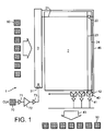
- a SRAM test chip 1 consists of a matrix memory array 2 which has an address register 3 connected to its plural wordlines 21, of which only one is shown.
- the wordlines 21 connect to a regular array of memory cells 22, of which again only one is shown.
- an exemplary memory cell 22 consists of two cross-coupled inverter circuits 26, 27; 28, 29.
- the left hand inverter as shown consists of a P channel FET 26 connected between a positive supply VDD and a first common node and an N channel FET 27 connected between the first common node and a negative supply VSS.
- the right hand inverter similarly consists of a second P conductivity FET 28 connected between the positive supply VDD and a second common node, and a second N channel FET 29 connected between the second common node and the negative supply VSS.
- the gates of the first P and first N transistors 26, 27 are connected together and to the second common node, and the gates of the second P transistor 28 and the second N transistor 29 are connected together and to the first common node.
- the first common node is connected via an N type pass transistor 24 to a first bitline 23 and the second common node is connected via a second N channel pass transistor 25 to a second bitline 24.
- the wordline 21 forms the gate connection to both the first and second pass transistors 24 and 25.
- the bitlines 23, 24 are complementary and form the column lines of the memory array whereas the wordlines form the row lines of the array.
- bitline 23 is connected to a logic 1 and bitline 24 to a logic 0
- the pass transistors 24, 25 will turn on and the cross-coupled inverters will latch into a corresponding state with the first common node at a high potential and the second common node at a low potential.
- the wordline is once again connected to a logic 1 and the pass transistors 24, 25 will then turn on causing the bitline potential to tend towards the respective potential of the common node to which it is connected.
- each pair of bitlines is connected to a respective sense amplifier 40.
- the outputs of the sense amplifiers 40 feed via buffers 41 to a corresponding number of output pads 50.
- An input to the address register 3 is provided from a plurality of input pads 60 and the address register itself is clocked at an address register clock input 31.
- An address register clock input pad 70 is connected to the address register clock input 31 via a circuit path containing the three series elements 71, 72, 73 which figuratively illustrate the delay entailed.
- the sense amplifiers 40 are also clocked, each having a clock terminal 42.
- a clock pulse line 46 is connected between the address register 3 and the sense amplifier clock terminal 42, and has a delay sufficient to ensure that the sense amplifier 40 will operate correctly, as later described herein.
- a clock signal 100 is provided at address register clock input pad 70. After passing through the series elements 71-73, the clock pulse becomes an internal clock pulse 101 at a time T1 after the instant of application of the clock pulse 100 at the pad 70.
- the time period T1 is the delay induced by the path comprising series elements 71-73.
- the action of the internal clock 101 on the address register 3 causes the register to apply a transition 102 to the wordlines 21 after a further time delay T2.
- This time delay T2 is predominantly due to the switching time of the address register 3.
- the transition 102 on the wordlines 21 causes the memory cells 22 to become connected to the complementary bitlines 23, 24.
- the bitlines 23, 24 have a relatively high capacitance and the memory cells 22 have a relatively low current driving capability which means that the change of potential of 104 is relatively slow.
- the sense amplifier 42 were activated before the differential between the complementary bitlines had achieved a sufficiently high value, the sense amplifier might latch into an incorrect state. Accordingly, a clock pulse 105 is applied to the clock input 42 of the sense amplifiers 40 at a time T3 where it is expected that the bitlines will have a sufficiently high differential voltage to ensure correct sensing. In turn, the sense amplifiers require a further interval T4 before the outputs at the output nodes of the buffers 41 have achieved a reliable level. Finally, the data output circuitry 43 causes a yet further delay T5 before the response to the access caused by the clock pulse 100 applied to terminal 70 is accessible at the output pads 50.
- the access time of the memory array 2 is defined as the period between the application of the clock pulse 101 at clock node 31 to the appearance of the data output at the buffer output node 41.
- access is normally available only to the input pads 60, 70 and the output pads 50. Measurements taken at these points will give a false access time measurement due to the inability to eliminate the time T1 and the final delay T5. This is especially serious where the memory 2 is a highly embedded memory due to the path length between the memory and the terminals.
- a device incorporating a first embodiment of the invention has clocked flip-flop circuitry 44 at the outputs from the buffers 41.
- the flip-flop circuitry 44 has a clock input 45 and is operable at the time of transition of the clock input 45 to store at its outputs the states pertaining at its inputs immediately before the clock pulse transition.
- the clock input 45 of the flip-flop circuitry 44 is provided with a clocking signal from a pad 75 via a path consisting of the series connection of elements 76, 77 and 78. These elements are so configured that the delay between the flip-flop circuitry clock pad 75 and clock input 45 is as near as possible equal to the delay between the address register clock input pad 70 and the clock input terminal 31 of the address register 3.
- the device further comprises a clock generator 80 which has two clock outputs 81, 82 the first clock output 81 being connected to the address register clock input pad 70 of the device and the clock output 82 being connected to the flip-flop circuitry clock pad 75 of the device.
- the clock circuit 80 is capable of generating the first clock signal 81 at selected intervals, each such generation being followed by generation of the second clock signal 82 at a controllable variable delay afterwards.
- the variable delay is controllably set to establish the access time of the memory array 2 as will now be described:-
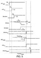
- a clock pulse 100 is applied from the first clock signal line 81 to the address register clock input pad 70 and after propagation along the path comprising elements 71, 72, 73 arrives at the clock input 31 of the address register 3 to form an internal clock signal 101 at a time T1.
- this results in the wordline transition 102 at time T2, differential bitline activation followed by sense amplifier clocking at time T3 and internal data determination at the outputs of buffers 41 at time T4.
Landscapes
- For Increasing The Reliability Of Semiconductor Memories (AREA)
- Tests Of Electronic Circuits (AREA)
Abstract
A method and device for measuring the response time of a circuit
are described in which clocking pulses are applied to the circuit
at input pads, the input pads being connected to the circuit by
circuitry having substantially the same delays. By adjusting the
timing of the later clock pulse relative to the earlier clock
pulse until a valid output is just achieved, the response time of
the circuit can be measured using a register circuit.
Description
The present invention relates to a device for measuring the
response time of a circuit and to a method of measuring the
response time of a circuit.
More particularly, but not exclusively the invention relates to a
method of determining the response time of a deeply embedded
memory, for example a static RAM and to a device for determining
the response time of a deeply embedded memory, for example a
static RAM.
Current techniques for evaluating embedded fast SRAM designs use
either extremely high performance testing devices, which are
costly or alternatively require physical access to internal
nodes. The latter tends to be inaccurate and is not capable of
providing statistical sampling over long periods of time.
It will be desirable to provide a method and device capable of
providing statistical data on a number of circuits and to use
conventional test apparatus to collect statistically significant
data.
According to a first aspect of the present invention there is
provided a device for measuring the response time of a circuit,
the circuit having an output for providing a response to a
stimulus at an input node thereof, the device comprising first
circuitry having a clock node and an output, said first circuitry
being connected to store an output condition, said output
condition corresponding to a state of said circuit output at the
time of occurrence of a clock pulse at said clock node, the
device further comprising second circuitry and third circuitry,
said second circuitry being responsive to a second circuitry
input signal at its input to provide said stimulus at said input
node of said circuit, and said third circuitry being responsive
to a third circuitry input signal at its input to provide a clock
pulse at said clock node whereby said response time is determined
by the time between said second circuitry input signal and said
third circuitry input signal, wherein said second circuitry has
an output connected to said input node, and said third circuitry
has an output connected to said clock node, and a delay between
the input to said second circuitry and its output is
substantially the same as a delay between the input and output of
the third circuitry.
Preferably, said circuit comprises a memory, having address latch
circuitry with a clock input as said circuit input node, an array
of memory cells coupled to said address latch circuitry and sense
amplifier circuitry connected to said array, said sense amplifier
circuitry having a sense amplifier output as said circuit output.
Advantageously said memory is an embedded memory.
Advantageously said embedded memory comprises a SRAM.
Advantageously the first circuitry comprises flip-flop circuitry.
According to a second aspect of the present invention there is
provided a device for measuring a response time of a circuit
between an input node and a circuit output thereof, wherein said
circuit output is connected via first connecting circuitry to an
output pad, said device comprising a first timing signal source
for providing a first timing signal to said input node via a
first path having a first delay, clocked circuitry having a clock
node and being connected at said circuit output, said clocked
circuitry having an output to said first connecting circuitry,
said clocked circuitry being responsive to a clock signal at said
clock node to provide to said first connecting circuitry a signal
existing at said circuit output immediately prior to the
occurrence of said clock signal, the device further comprising a
second timing signal source for providing a second timing signal
as said clock signal to said clock node via a second path having
a second delay substantially equal to said first delay, and means
for determining a time period between said first and second
timing signals.
Advantageously said clocked circuitry comprises a flip-flop.
Preferably the device further comprises a sensing device
connected to said output pad for sensing a desired output
thereat.
Preferably again said circuit comprises a static RAM.
Conveniently said static RAM comprises address latch circuitry
having a latch clock node as said input node, an array of memory
cells coupled to said address latch circuitry, and sense
amplifier circuitry having a sense amplifier output node as said
output node.
According to a further aspect of the present invention there is
provided a method of measuring the response time of a circuit
having a circuit output for providing an output in response to a
stimulus applied to a circuit input, the circuit input being
connected to a first input pad via first circuitry having a
predetermined delay, the method comprising:-
Preferably said second circuitry is coupled to an output pad, and
said determining step comprises monitoring said output pad.
Advantageously said desired output condition is a valid condition
such that reduction of said variable delay produces an invalid
condition.
Embodiments of the invention will now be described, by way of
example only, with reference to the accompanying drawings in
which:-
In the various figures, like reference numerals refer to like
parts.
Referring first to Figure 1 a SRAM test chip 1 consists of a
matrix memory array 2 which has an address register 3 connected
to its plural wordlines 21, of which only one is shown. The
wordlines 21 connect to a regular array of memory cells 22, of
which again only one is shown.
Referring now to Figure 2, an exemplary memory cell 22 consists
of two cross-coupled inverter circuits 26, 27; 28, 29. The left
hand inverter as shown consists of a P channel FET 26 connected
between a positive supply VDD and a first common node and an N
channel FET 27 connected between the first common node and a
negative supply VSS. The right hand inverter, as shown,
similarly consists of a second P conductivity FET 28 connected
between the positive supply VDD and a second common node, and a
second N channel FET 29 connected between the second common node
and the negative supply VSS. The gates of the first P and first
N transistors 26, 27 are connected together and to the second
common node, and the gates of the second P transistor 28 and the
second N transistor 29 are connected together and to the first
common node. The first common node is connected via an N type
pass transistor 24 to a first bitline 23 and the second common
node is connected via a second N channel pass transistor 25 to a
second bitline 24. The wordline 21 forms the gate connection to
both the first and second pass transistors 24 and 25. As is
known to those skilled in the art the bitlines 23, 24 are
complementary and form the column lines of the memory array
whereas the wordlines form the row lines of the array.
In operation, information is written into the memory cell 22 by
providing a differential potential on the bitlines 23, 24. If
for example bitline 23 is connected to a logic 1 and bitline 24
to a logic 0, then when the wordline 21 goes logic 1 the pass
transistors 24, 25 will turn on and the cross-coupled inverters
will latch into a corresponding state with the first common node
at a high potential and the second common node at a low
potential. To read from the memory the wordline is once again
connected to a logic 1 and the pass transistors 24, 25 will then
turn on causing the bitline potential to tend towards the
respective potential of the common node to which it is connected.
Returning again to Figure 1, each pair of bitlines is connected
to a respective sense amplifier 40. The outputs of the sense
amplifiers 40 feed via buffers 41 to a corresponding number of
output pads 50.
In the illustrated memory, 32 pairs of bitlines are provided and
thus there are 32 sense amplifiers 40, connected to 32 output
terminals 50 via output circuitry 43.
An input to the address register 3 is provided from a plurality
of input pads 60 and the address register itself is clocked at an
address register clock input 31. An address register clock input
pad 70 is connected to the address register clock input 31 via a
circuit path containing the three series elements 71, 72, 73
which figuratively illustrate the delay entailed.
Thesense amplifiers 40 are also clocked, each having a clock
terminal 42. A clock pulse line 46 is connected between the
address register 3 and the sense amplifier clock terminal 42, and
has a delay sufficient to ensure that the sense amplifier 40 will
operate correctly, as later described herein.
The
Referring now to Figure 3, in operation, a clock signal 100 is
provided at address register clock input pad 70. After passing
through the series elements 71-73, the clock pulse becomes an
internal clock pulse 101 at a time T1 after the instant of
application of the clock pulse 100 at the pad 70. The time
period T1 is the delay induced by the path comprising series
elements 71-73.
The action of the internal clock 101 on the address register 3
causes the register to apply a transition 102 to the wordlines 21
after a further time delay T2. This time delay T2 is
predominantly due to the switching time of the address register
3.
As previously discussed, the transition 102 on the wordlines 21
causes the memory cells 22 to become connected to the
complementary bitlines 23, 24. The bitlines 23, 24 have a
relatively high capacitance and the memory cells 22 have a
relatively low current driving capability which means that the
change of potential of 104 is relatively slow. If the sense
amplifier 42 were activated before the differential between the
complementary bitlines had achieved a sufficiently high value,
the sense amplifier might latch into an incorrect state.
Accordingly, a clock pulse 105 is applied to the clock input 42
of the sense amplifiers 40 at a time T3 where it is expected that
the bitlines will have a sufficiently high differential voltage
to ensure correct sensing. In turn, the sense amplifiers require
a further interval T4 before the outputs at the output nodes of
the buffers 41 have achieved a reliable level. Finally, the data
output circuitry 43 causes a yet further delay T5 before the
response to the access caused by the clock pulse 100 applied to
terminal 70 is accessible at the output pads 50.
The access time of the memory array 2 is defined as the period
between the application of the clock pulse 101 at clock node 31
to the appearance of the data output at the buffer output node
41. Where the memory 2 is embedded, access is normally available
only to the input pads 60, 70 and the output pads 50.
Measurements taken at these points will give a false access time
measurement due to the inability to eliminate the time T1 and the
final delay T5. This is especially serious where the memory 2 is
a highly embedded memory due to the path length between the
memory and the terminals.
Referring now to Figure 4 a device incorporating a first
embodiment of the invention has clocked flip-flop circuitry 44 at
the outputs from the buffers 41. The flip-flop circuitry 44 has
a clock input 45 and is operable at the time of transition of the
clock input 45 to store at its outputs the states pertaining at
its inputs immediately before the clock pulse transition. The
clock input 45 of the flip-flop circuitry 44 is provided with a
clocking signal from a pad 75 via a path consisting of the series
connection of elements 76, 77 and 78. These elements are so
configured that the delay between the flip-flop circuitry clock
pad 75 and clock input 45 is as near as possible equal to the
delay between the address register clock input pad 70 and the
clock input terminal 31 of the address register 3.
The device further comprises a clock generator 80 which has two
clock outputs 81, 82 the first clock output 81 being connected to
the address register clock input pad 70 of the device and the
clock output 82 being connected to the flip-flop circuitry clock
pad 75 of the device. The clock circuit 80 is capable of
generating the first clock signal 81 at selected intervals, each
such generation being followed by generation of the second clock
signal 82 at a controllable variable delay afterwards. The
variable delay is controllably set to establish the access time
of the memory array 2 as will now be described:-
Referring now to Figure 5 a clock pulse 100 is applied from the
first clock signal line 81 to the address register clock input
pad 70 and after propagation along the path comprising elements
71, 72, 73 arrives at the clock input 31 of the address register
3 to form an internal clock signal 101 at a time T1. As
previously described with respect to Figure 3, this results in
the wordline transition 102 at time T2, differential bitline
activation followed by sense amplifier clocking at time T3 and
internal data determination at the outputs of buffers 41 at time
T4.
Transmission of the state at the output of the buffers 41 to the
circuit output pads 50 will only occur if a second clock pulse
from the second clock signal line 82 is applied to the flip-flop
circuitry clock terminal pad 75 to arrive at the clock terminal
45 of the flip-flop circuitry 44 after the buffers 41 have
produced their output. If a clock pulse is applied to the clock
input 45 of the flip-flop circuitry 44 at the instant that the
buffers 41 produce their output, then the access time of the
memory is equal to the period between the application of the
internal clock to the address buffer 3 and the application of the
second internal clock to the clock node 45. Such a period is not
itself directly capable of measurement, but it will be recalled
that the time delay of the path from address register clock input
pad 70 to the clock input 31 of the address register 3 is, in
this embodiment, identical to the delay between flip-flop clock
input pad 75 and clock input 45 of the flip-flop circuitry 44.
Hence the time spacing between application of the first clock to
the clock input pad 70 and application of that second clock 110
to clock input pad 75 which give rise to the second internal
clock being coincident with the output from buffers 41, is equal
to the memory access time.
It will thus be clear that if the memory is successively accessed
with an ever increasing time difference between application of
the first and second clocks, then that time spacing which first
allows the output conditions to reach the output pads 50 will
correspond to the access time of the circuit. Similarly, if the
memory is successfully accessed with an ever decreasing time
difference between application of the first and second clocks,
then that time spacing which last allows the output conditions to
reach the output pads 50 will correspond to the access time of
the circuit.
Those skilled in the art will be aware that because measurement
is made only at the external connection pads of the circuit
arrangement, there is no requirement to obtain physical access to
internal nodes. Similarly, since it is only the accuracy with
which the rising edges of two clock pulses are placed that is
important, it is not necessary to use a high performance testing
device.
Claims (13)
- A device for measuring the response time of a circuit, the circuit having an output for providing a response to a stimulus at an input node thereof, the device comprising first circuitry having a clock node and an output, said first circuitry being connected to store an output condition, said output condition corresponding to a state of said circuit output at the time of occurrence of a clock pulse at said clock node, the device further comprising second circuitry and third circuitry, said second circuitry being responsive to a second circuitry input signal at its input to provide said stimulus at said input node of said circuit, and said third circuitry being responsive to a third circuitry input signal at its input to provide a clock pulse at said clock node whereby said response time is determined by the time between said second circuitry input signal and said third circuitry input signal, wherein said second circuitry has an output connected to said input node, and said third circuitry has an output connected to said clock node, and a delay between the input to said second circuitry and its output is substantially the same as a delay between the input and output of the third circuitry.
- The device of claim 1 wherein said circuit comprises a memory, having address latch circuitry with a clock input as said circuit input node, an array of memory cells coupled to said address latch circuitry and sense amplifier circuitry connected to said array, said sense amplifier circuitry having a sense amplifier output as said circuit output.
- The device of claim 2 wherein said memory is an embedded memory.
- The device of claim 3 wherein said embedded memory comprises a SRAM.
- The device of any preceding claim wherein the first circuitry comprises flip-flop circuitry.
- A device for measuring a response time of a circuit between an input node and a circuit output thereof, wherein said circuit output is connected via first connecting circuitry to an output pad, said device comprising a first timing signal source for providing a first timing signal to said input node via a first path having a first delay, clocked circuitry having a clock node and being connected at said circuit output, said clocked circuitry having an output to said first connecting circuitry, said clocked circuitry being responsive to a clock signal at said clock node to provide to said first connecting circuitry a signal existing at said circuit output immediately prior to the occurrence of said clock signal, the device further comprising a second timing signal source for providing a second timing signal as said clock signal to said clock node via a second path having a second delay substantially equal to said first delay, and means for determining a time period between said first and second timing signals.
- The device of claim 6 wherein said clock circuitry comprises a flip-flop.
- The device of claim 6 or claim 7 and further comprising a sensing device connected to said output pad for sensing a desired output thereat.
- The device of any of claims 6-8 wherein said circuit comprises a static RAM.
- The device of claim 9 wherein said static RAM comprises address latch circuitry having a latch clock node as said input node, an array of memory cells coupled to said address latch circuitry, and sense amplifier circuitry having a sense amplifier output node as said output node.
- A method of measuring the response time of a circuit having a circuit output for providing an output in response to a stimulus applied to a circuit input, the circuit input being connected to a first input pad via first circuitry having a predetermined delay, the method comprising: providing second circuitry having a clock node, said clock node being connected to a second input pad via third circuitry, said third circuitry having said predetermined delay, and said second circuitry having an output for storing an output condition, said output condition corresponding to the state of said circuit output at the time of occurrence of a clock pulse at said clock node; repeatedly applying a stimulus to said first input pad and at a variable delay after each application, providing a clock pulse to said second input pad; and determining, as said response time, a value of said variable delay corresponding to a desired output condition of said second circuitry.
- A method of claim 11 wherein said second circuitry is coupled to an output pad, and said determining step comprises monitoring said output pad.
- The method of claim 11 or 12 wherein said desired output condition is a valid condition such that reduction of said variable delay produces an invalid condition.
Applications Claiming Priority (2)
| Application Number | Priority Date | Filing Date | Title |
|---|---|---|---|
| GB9910942 | 1999-05-11 | ||
| GBGB9910942.3A GB9910942D0 (en) | 1999-05-11 | 1999-05-11 | Response time measurement |
Publications (1)
| Publication Number | Publication Date |
|---|---|
| EP1052648A1 true EP1052648A1 (en) | 2000-11-15 |
Family
ID=10853253
Family Applications (1)
| Application Number | Title | Priority Date | Filing Date |
|---|---|---|---|
| EP00302836A Withdrawn EP1052648A1 (en) | 1999-05-11 | 2000-04-04 | Response time measurement |
Country Status (3)
| Country | Link |
|---|---|
| US (1) | US6584577B1 (en) |
| EP (1) | EP1052648A1 (en) |
| GB (1) | GB9910942D0 (en) |
Families Citing this family (2)
| Publication number | Priority date | Publication date | Assignee | Title |
|---|---|---|---|---|
| US7310752B2 (en) * | 2003-09-12 | 2007-12-18 | Micron Technology, Inc. | System and method for on-board timing margin testing of memory modules |
| US7120743B2 (en) | 2003-10-20 | 2006-10-10 | Micron Technology, Inc. | Arbitration system and method for memory responses in a hub-based memory system |
Citations (5)
| Publication number | Priority date | Publication date | Assignee | Title |
|---|---|---|---|---|
| EP0867887A2 (en) * | 1997-03-14 | 1998-09-30 | Texas Instruments Incorporated | Memory access time measurement circuit and method |
| US5822228A (en) * | 1997-05-27 | 1998-10-13 | Lsi Logic Corporation | Method for using built in self test to characterize input-to-output delay time of embedded cores and other integrated circuits |
| US5825712A (en) * | 1996-08-19 | 1998-10-20 | Kabushiki Kaisha Toshiba | Semiconductor integrated circuit |
| US5875135A (en) * | 1995-12-28 | 1999-02-23 | Intel Corporation | Characterization of self time circuit |
| EP0898284A2 (en) * | 1997-07-31 | 1999-02-24 | Nec Corporation | Semiconductor memory having a test circuit |
Family Cites Families (9)
| Publication number | Priority date | Publication date | Assignee | Title |
|---|---|---|---|---|
| US4736351A (en) * | 1986-08-28 | 1988-04-05 | Oliver Douglas E | Precision semiconductor device timer |
| JPH02184048A (en) * | 1989-01-11 | 1990-07-18 | Mitsubishi Electric Corp | Semiconductor integrated circuit having built-in memory |
| JPH0792235A (en) * | 1993-09-25 | 1995-04-07 | Nec Corp | Semiconductor device and method for measuring delay time of the device |
| US5537663A (en) * | 1993-10-29 | 1996-07-16 | Compaq Computer Corporation | System for determining configuration of devices installed on a computer bus by comparing response time of data lines to read from I/O address when undriven |
| US5611045A (en) * | 1993-10-29 | 1997-03-11 | Compaq Computer Corporation | Detecting the presence of a device on a computer system bus by measuring the response time of data signals on the bus, and maximizing system performance based on that response time |
| US5821760A (en) * | 1996-07-31 | 1998-10-13 | Fluke Corporation | Method and apparatus for measuring near-end cross-talk in patch cords |
| US5751727A (en) * | 1997-03-20 | 1998-05-12 | International Business Machines Corporation | Dynamic latch circuit for utilization with high-speed memory arrays |
| US6154821A (en) * | 1998-03-10 | 2000-11-28 | Rambus Inc. | Method and apparatus for initializing dynamic random access memory (DRAM) devices by levelizing a read domain |
| US6185637B1 (en) * | 1998-04-15 | 2001-02-06 | Advanced Micro Devices, Inc. | System for implementing an adaptive burst length for burst mode transactions of a memory by monitoring response times for different memory regions |
-
1999
- 1999-05-11 GB GBGB9910942.3A patent/GB9910942D0/en not_active Ceased
-
2000
- 2000-04-04 EP EP00302836A patent/EP1052648A1/en not_active Withdrawn
- 2000-04-11 US US09/546,809 patent/US6584577B1/en not_active Expired - Lifetime
Patent Citations (5)
| Publication number | Priority date | Publication date | Assignee | Title |
|---|---|---|---|---|
| US5875135A (en) * | 1995-12-28 | 1999-02-23 | Intel Corporation | Characterization of self time circuit |
| US5825712A (en) * | 1996-08-19 | 1998-10-20 | Kabushiki Kaisha Toshiba | Semiconductor integrated circuit |
| EP0867887A2 (en) * | 1997-03-14 | 1998-09-30 | Texas Instruments Incorporated | Memory access time measurement circuit and method |
| US5822228A (en) * | 1997-05-27 | 1998-10-13 | Lsi Logic Corporation | Method for using built in self test to characterize input-to-output delay time of embedded cores and other integrated circuits |
| EP0898284A2 (en) * | 1997-07-31 | 1999-02-24 | Nec Corporation | Semiconductor memory having a test circuit |
Also Published As
| Publication number | Publication date |
|---|---|
| GB9910942D0 (en) | 1999-07-14 |
| US6584577B1 (en) | 2003-06-24 |
Similar Documents
| Publication | Publication Date | Title |
|---|---|---|
| KR100478764B1 (en) | On-chip test circuit for measuring on-chip signals using external test signals | |
| EP0128499B1 (en) | Mos memory | |
| KR100203529B1 (en) | Dynamic semiconductor memory and its test method | |
| US6762967B2 (en) | Semiconductor memory device having a circuit for fast operation | |
| KR960003533B1 (en) | Semiconductor memory device including address transition detector | |
| KR950034253A (en) | Synchronous Memory with Parallel Output Data Path | |
| KR100288516B1 (en) | Semiconductor memory | |
| US6396754B1 (en) | Semiconductor memory device which controls sense amplifier for detecting bit line bridge and method of controlling the semiconductor memory device | |
| US6034904A (en) | Semiconductor memory device having selection circuit for arbitrarily setting a word line to selected state at high speed in test mode | |
| US5889709A (en) | Data latch circuit device with flip-flop of semi-conductor memory of synchronous DRAM | |
| KR930001652B1 (en) | Semiconductor memory device | |
| US5007028A (en) | Multiport memory with improved timing of word line selection | |
| US6359816B1 (en) | Response time measurement | |
| US6584577B1 (en) | System for measuring response time of a circuit by determining the time difference between the earlier and the later clock pulses applied to the circuit | |
| KR100311175B1 (en) | Semiconductor memory | |
| JP3827749B2 (en) | Synchronous memory with parallel output data path | |
| EP0220577B1 (en) | Memory array | |
| US6604213B1 (en) | Method and apparatus for determining a minimum clock delay in a memory | |
| US6628559B2 (en) | Semiconductor memory device having refreshing function | |
| KR100543226B1 (en) | Semiconductor memory device with test mode | |
| US5629896A (en) | Write controlled address buffer | |
| US20030128613A1 (en) | Semiconductor memory device capable of measuring a period of an internally produced periodic signal | |
| US6111813A (en) | Apparatus and method for tracking dynamic sense amplifier enable signals with memory array accessing signals in a synchronous RAM | |
| US6654937B1 (en) | Register file timing using static timing tools | |
| Joshi et al. | High performance SRAMs in 1.5 V, 0.18/spl mu/m partially depleted SOI technology |
Legal Events
| Date | Code | Title | Description |
|---|---|---|---|
| PUAI | Public reference made under article 153(3) epc to a published international application that has entered the european phase |
Free format text: ORIGINAL CODE: 0009012 |
|
| AK | Designated contracting states |
Kind code of ref document: A1 Designated state(s): DE FR GB IT |
|
| AX | Request for extension of the european patent |
Free format text: AL;LT;LV;MK;RO;SI |
|
| 17P | Request for examination filed |
Effective date: 20010330 |
|
| AKX | Designation fees paid |
Free format text: DE FR GB IT |
|
| 17Q | First examination report despatched |
Effective date: 20060720 |
|
| STAA | Information on the status of an ep patent application or granted ep patent |
Free format text: STATUS: THE APPLICATION IS DEEMED TO BE WITHDRAWN |
|
| 18D | Application deemed to be withdrawn |
Effective date: 20070131 |