EP1049241A2 - Modified space vector pulse width modulation technique to reduce DC bus ripple effect in voltage source inverters - Google Patents
Modified space vector pulse width modulation technique to reduce DC bus ripple effect in voltage source inverters Download PDFInfo
- Publication number
- EP1049241A2 EP1049241A2 EP00303628A EP00303628A EP1049241A2 EP 1049241 A2 EP1049241 A2 EP 1049241A2 EP 00303628 A EP00303628 A EP 00303628A EP 00303628 A EP00303628 A EP 00303628A EP 1049241 A2 EP1049241 A2 EP 1049241A2
- Authority
- EP
- European Patent Office
- Prior art keywords
- voltage
- ripple
- phase
- pulse width
- instantaneous
- Prior art date
- Legal status (The legal status is an assumption and is not a legal conclusion. Google has not performed a legal analysis and makes no representation as to the accuracy of the status listed.)
- Granted
Links
- 230000000694 effects Effects 0.000 title claims abstract description 15
- 239000013598 vector Substances 0.000 title claims description 30
- 238000000034 method Methods 0.000 title claims description 16
- 239000003990 capacitor Substances 0.000 claims abstract description 19
- 230000001419 dependent effect Effects 0.000 claims 2
- 238000006243 chemical reaction Methods 0.000 abstract description 11
- 238000013459 approach Methods 0.000 abstract description 2
- 230000006698 induction Effects 0.000 abstract description 2
- 230000006870 function Effects 0.000 description 9
- 230000007935 neutral effect Effects 0.000 description 5
- 238000001228 spectrum Methods 0.000 description 5
- 230000000295 complement effect Effects 0.000 description 4
- 238000001914 filtration Methods 0.000 description 4
- 230000004044 response Effects 0.000 description 3
- 238000010586 diagram Methods 0.000 description 2
- 230000014509 gene expression Effects 0.000 description 2
- 230000009467 reduction Effects 0.000 description 2
- 101100162020 Mesorhizobium japonicum (strain LMG 29417 / CECT 9101 / MAFF 303099) adc3 gene Proteins 0.000 description 1
- 101100434411 Saccharomyces cerevisiae (strain ATCC 204508 / S288c) ADH1 gene Proteins 0.000 description 1
- 101150102866 adc1 gene Proteins 0.000 description 1
- 238000004364 calculation method Methods 0.000 description 1
- 230000015556 catabolic process Effects 0.000 description 1
- 238000005094 computer simulation Methods 0.000 description 1
- 238000012937 correction Methods 0.000 description 1
- 230000003247 decreasing effect Effects 0.000 description 1
- 238000006731 degradation reaction Methods 0.000 description 1
- 230000008030 elimination Effects 0.000 description 1
- 238000003379 elimination reaction Methods 0.000 description 1
- 238000009432 framing Methods 0.000 description 1
- 230000036039 immunity Effects 0.000 description 1
- 230000006872 improvement Effects 0.000 description 1
- 238000005259 measurement Methods 0.000 description 1
- 238000012986 modification Methods 0.000 description 1
- 230000004048 modification Effects 0.000 description 1
- 230000008450 motivation Effects 0.000 description 1
- 238000012545 processing Methods 0.000 description 1
- 238000005070 sampling Methods 0.000 description 1
- 238000004088 simulation Methods 0.000 description 1
Images


Classifications
-
- H—ELECTRICITY
- H02—GENERATION; CONVERSION OR DISTRIBUTION OF ELECTRIC POWER
- H02M—APPARATUS FOR CONVERSION BETWEEN AC AND AC, BETWEEN AC AND DC, OR BETWEEN DC AND DC, AND FOR USE WITH MAINS OR SIMILAR POWER SUPPLY SYSTEMS; CONVERSION OF DC OR AC INPUT POWER INTO SURGE OUTPUT POWER; CONTROL OR REGULATION THEREOF
- H02M7/00—Conversion of AC power input into DC power output; Conversion of DC power input into AC power output
- H02M7/42—Conversion of DC power input into AC power output without possibility of reversal
- H02M7/44—Conversion of DC power input into AC power output without possibility of reversal by static converters
- H02M7/48—Conversion of DC power input into AC power output without possibility of reversal by static converters using discharge tubes with control electrode or semiconductor devices with control electrode
- H02M7/53—Conversion of DC power input into AC power output without possibility of reversal by static converters using discharge tubes with control electrode or semiconductor devices with control electrode using devices of a triode or transistor type requiring continuous application of a control signal
- H02M7/537—Conversion of DC power input into AC power output without possibility of reversal by static converters using discharge tubes with control electrode or semiconductor devices with control electrode using devices of a triode or transistor type requiring continuous application of a control signal using semiconductor devices only, e.g. single switched pulse inverters
- H02M7/5387—Conversion of DC power input into AC power output without possibility of reversal by static converters using discharge tubes with control electrode or semiconductor devices with control electrode using devices of a triode or transistor type requiring continuous application of a control signal using semiconductor devices only, e.g. single switched pulse inverters in a bridge configuration
- H02M7/53871—Conversion of DC power input into AC power output without possibility of reversal by static converters using discharge tubes with control electrode or semiconductor devices with control electrode using devices of a triode or transistor type requiring continuous application of a control signal using semiconductor devices only, e.g. single switched pulse inverters in a bridge configuration with automatic control of output voltage or current
- H02M7/53875—Conversion of DC power input into AC power output without possibility of reversal by static converters using discharge tubes with control electrode or semiconductor devices with control electrode using devices of a triode or transistor type requiring continuous application of a control signal using semiconductor devices only, e.g. single switched pulse inverters in a bridge configuration with automatic control of output voltage or current with analogue control of three-phase output
-
- H—ELECTRICITY
- H02—GENERATION; CONVERSION OR DISTRIBUTION OF ELECTRIC POWER
- H02M—APPARATUS FOR CONVERSION BETWEEN AC AND AC, BETWEEN AC AND DC, OR BETWEEN DC AND DC, AND FOR USE WITH MAINS OR SIMILAR POWER SUPPLY SYSTEMS; CONVERSION OF DC OR AC INPUT POWER INTO SURGE OUTPUT POWER; CONTROL OR REGULATION THEREOF
- H02M7/00—Conversion of AC power input into DC power output; Conversion of DC power input into AC power output
- H02M7/42—Conversion of DC power input into AC power output without possibility of reversal
- H02M7/44—Conversion of DC power input into AC power output without possibility of reversal by static converters
- H02M7/48—Conversion of DC power input into AC power output without possibility of reversal by static converters using discharge tubes with control electrode or semiconductor devices with control electrode
- H02M7/505—Conversion of DC power input into AC power output without possibility of reversal by static converters using discharge tubes with control electrode or semiconductor devices with control electrode using devices of a thyratron or thyristor type requiring extinguishing means
- H02M7/515—Conversion of DC power input into AC power output without possibility of reversal by static converters using discharge tubes with control electrode or semiconductor devices with control electrode using devices of a thyratron or thyristor type requiring extinguishing means using semiconductor devices only
- H02M7/525—Conversion of DC power input into AC power output without possibility of reversal by static converters using discharge tubes with control electrode or semiconductor devices with control electrode using devices of a thyratron or thyristor type requiring extinguishing means using semiconductor devices only with automatic control of output waveform or frequency
- H02M7/527—Conversion of DC power input into AC power output without possibility of reversal by static converters using discharge tubes with control electrode or semiconductor devices with control electrode using devices of a thyratron or thyristor type requiring extinguishing means using semiconductor devices only with automatic control of output waveform or frequency by pulse width modulation
-
- H—ELECTRICITY
- H02—GENERATION; CONVERSION OR DISTRIBUTION OF ELECTRIC POWER
- H02M—APPARATUS FOR CONVERSION BETWEEN AC AND AC, BETWEEN AC AND DC, OR BETWEEN DC AND DC, AND FOR USE WITH MAINS OR SIMILAR POWER SUPPLY SYSTEMS; CONVERSION OF DC OR AC INPUT POWER INTO SURGE OUTPUT POWER; CONTROL OR REGULATION THEREOF
- H02M1/00—Details of apparatus for conversion
- H02M1/14—Arrangements for reducing ripples from DC input or output
-
- H—ELECTRICITY
- H02—GENERATION; CONVERSION OR DISTRIBUTION OF ELECTRIC POWER
- H02P—CONTROL OR REGULATION OF ELECTRIC MOTORS, ELECTRIC GENERATORS OR DYNAMO-ELECTRIC CONVERTERS; CONTROLLING TRANSFORMERS, REACTORS OR CHOKE COILS
- H02P27/00—Arrangements or methods for the control of AC motors characterised by the kind of supply voltage
- H02P27/04—Arrangements or methods for the control of AC motors characterised by the kind of supply voltage using variable-frequency supply voltage, e.g. inverter or converter supply voltage
- H02P27/06—Arrangements or methods for the control of AC motors characterised by the kind of supply voltage using variable-frequency supply voltage, e.g. inverter or converter supply voltage using DC to AC converters or inverters
- H02P27/08—Arrangements or methods for the control of AC motors characterised by the kind of supply voltage using variable-frequency supply voltage, e.g. inverter or converter supply voltage using DC to AC converters or inverters with pulse width modulation
-
- H—ELECTRICITY
- H02—GENERATION; CONVERSION OR DISTRIBUTION OF ELECTRIC POWER
- H02M—APPARATUS FOR CONVERSION BETWEEN AC AND AC, BETWEEN AC AND DC, OR BETWEEN DC AND DC, AND FOR USE WITH MAINS OR SIMILAR POWER SUPPLY SYSTEMS; CONVERSION OF DC OR AC INPUT POWER INTO SURGE OUTPUT POWER; CONTROL OR REGULATION THEREOF
- H02M7/00—Conversion of AC power input into DC power output; Conversion of DC power input into AC power output
- H02M7/42—Conversion of DC power input into AC power output without possibility of reversal
- H02M7/44—Conversion of DC power input into AC power output without possibility of reversal by static converters
- H02M7/48—Conversion of DC power input into AC power output without possibility of reversal by static converters using discharge tubes with control electrode or semiconductor devices with control electrode
- H02M7/53—Conversion of DC power input into AC power output without possibility of reversal by static converters using discharge tubes with control electrode or semiconductor devices with control electrode using devices of a triode or transistor type requiring continuous application of a control signal
- H02M7/537—Conversion of DC power input into AC power output without possibility of reversal by static converters using discharge tubes with control electrode or semiconductor devices with control electrode using devices of a triode or transistor type requiring continuous application of a control signal using semiconductor devices only, e.g. single switched pulse inverters
- H02M7/5387—Conversion of DC power input into AC power output without possibility of reversal by static converters using discharge tubes with control electrode or semiconductor devices with control electrode using devices of a triode or transistor type requiring continuous application of a control signal using semiconductor devices only, e.g. single switched pulse inverters in a bridge configuration
- H02M7/53871—Conversion of DC power input into AC power output without possibility of reversal by static converters using discharge tubes with control electrode or semiconductor devices with control electrode using devices of a triode or transistor type requiring continuous application of a control signal using semiconductor devices only, e.g. single switched pulse inverters in a bridge configuration with automatic control of output voltage or current
- H02M7/53875—Conversion of DC power input into AC power output without possibility of reversal by static converters using discharge tubes with control electrode or semiconductor devices with control electrode using devices of a triode or transistor type requiring continuous application of a control signal using semiconductor devices only, e.g. single switched pulse inverters in a bridge configuration with automatic control of output voltage or current with analogue control of three-phase output
- H02M7/53876—Conversion of DC power input into AC power output without possibility of reversal by static converters using discharge tubes with control electrode or semiconductor devices with control electrode using devices of a triode or transistor type requiring continuous application of a control signal using semiconductor devices only, e.g. single switched pulse inverters in a bridge configuration with automatic control of output voltage or current with analogue control of three-phase output based on synthesising a desired voltage vector via the selection of appropriate fundamental voltage vectors, and corresponding dwelling times
Definitions
- the technical field of this invention is electric motor control.
- Power converters of the AC-DC-AC type are widely used in motor drives and power supply applications. These AC-DC-AC converters consist of a rectifier-inverter system along with a DC voltage link.
- the DC link is normally equipped with a large electrolytic capacitor which provides the stiff ripple free DC bus voltage required for proper inverter operation.
- this DC link capacitor is a large, heavy, and expensive component which continues to be a matter of concern in the industrial environment.
- the DC bus capacitor is the prime factor in degradation of system reliability. This has been the driving motivation for much work aimed at decreasing the required size of this DC link capacitor.
- Pulse Width Modulation (PWM) techniques have long been used to improve the performance and reliability of power conversion devices. Within the past decade such devices have improved steadily, yet the capacitor size and expense issue, as well as the reliability issue have remained paramount. This invention provides another level of improvement in power conversion devices by unique modifications to the PWM technique.
- PWM in its basic form as applied to power inverters is illustrated in Figure 1, the schematic of a conventional three-phase voltage source inverter.
- the diode bridge rectifier circuit (components 151, 152, 153, and 154) receives its power input from the AC power source 140, and its output is partially filtered by means of the DC link capacitor 150.
- the phase A, phase B, and phase C inverter outputs are derived from the inverter configuration comprised of N-channel MOSFET transistors 100 to 102 and 110 to 112. These output signals appear at the three nodes 190, 191 and 192.
- Providing appropriate drive signals for the gates of transistors 100 to 102 and 110 to 112 is the key to generating proper inverter output voltage.
- Diodes 160 to 162 and 170 to 172 act to clip any occurrences of reverse voltage at the drain to source of the inverter transistors 100 to 102 and 110 to 112.
- the line to line voltage at the inverter output is given by:
- Equation 9 represents the inverter line to line voltage with a ripple component in the DC bus voltage.
- equation 9 is identical to equation 2, in which the DC bus voltage was assumed to be ripple free. Therefore, by employing the proposed technique, i.e. by suitably altering the inverter switching function (SW), immunity to the DC bus voltage ripple component can be achieved.
- the conventional space vector PWM technique is modified to meet that goal.
- PWM Pulse Width Modulation
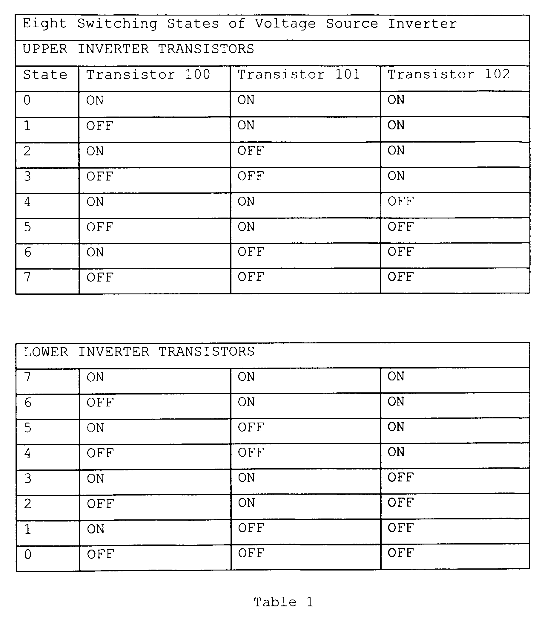
- Each inverter state represents a single combination of the states of inverter switching transistors 100 to 102. Any one, two or all three of these transistors may be 'on' in the eight possible combinations given in Table 1.
- the state of each of the complementary transistors 110 to 112 is the opposite. For example if transistor 100 is 'on', transistor 110 is 'off', and so on for transistor complementary pairs 101, the complement of 111, and transistor 102, the complement of transistor 112.
- the eight vectors of Figure 2 relate to the instantaneous inverter states of Table 1.
- the space vector PWM illustration of Figure 2 shows the space vectors of the line to neutral voltages of such an inverter.
- the voltage source inverter of Figure 2 can generate eight total states. Six of these states (v 1 through v 6 ) are non-zero vectors. The remaining vectors (v 0 and v 7 ) are zero states. They can occur only when all three upper (or lower) inverter switches are 'on'.
- the non-zero base vectors divide the cycle into six, 60° wide sectors.
- the simple algebraic formulas of equation 18 through 20 allow duty ratios of the consecutive logic states of an inverter to be computed in real time.
- the present invention provides a method for space vector pulse width modulation drive of a motor from a rectified AC input voltage comprising the steps of:
- the present invention exploits a Modified Space Vector Pulse Width Modulation (PWM) technique which results in improved multi-phase inverter operation in both power supply and motor drive applications and gives this improved performance while allowing for the reduction in the size of the expensive and large size capacitor which is normally required for filtering ripple on the DC bus voltage line.
- PWM Modified Space Vector Pulse Width Modulation
- equations 1 through 20 make the assumption that the inverter DC bus voltage has a 'stiffness' quality, namely, that is has no fluctuation. This may or may not be true in the real case. This is especially so when a small DC bus capacitor is used, and the DC bus voltage is clearly not ripple-free.
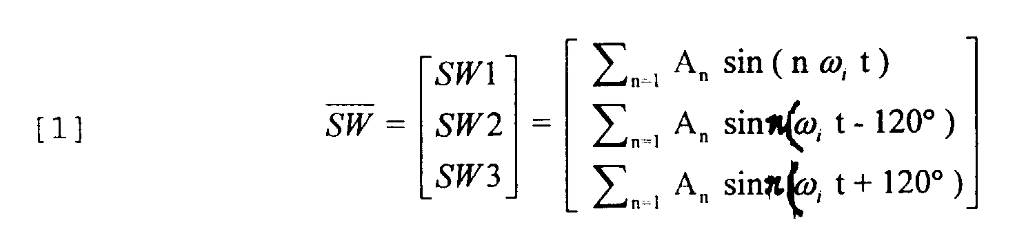
- the equations for implementing a modified form of space vector PWM include expressions for the modified duty-cycle values which the invention uses to effect a continual update of system duty cycle in order to minimize the effect of DC bus voltage ripple.
- a system diagram of the present invention shows how the measurement of DC bus voltage ripple can be used to generate a correction, by way of feedback through a controller device to modify instantaneous system duty cycle, thereby acting to reduce ripple effects for a given capacitor size.
- V DC K ripple V ripple
- Figure 5 shows a case for which PWM inverter drive inputs, equal to the desired PWM drive inputs, calculated from equations 24 and 25 of this invention, are applied for effective ripple effect cancellation.
- the frequency spectrum components show only the fundamental frequency range and the twenty-third harmonic range, and no 'distortion' or 'ripple' effects. These have been counteracted by modified PWM and resulting in full ripple-effect cancellation.
- the digital signal processor TMS320F240 a low cost fixed point DSP designed for motor control applications provides a means for applying the modified PWM technique of this invention. This is accomplished by driving the inverter input gates 120, 121, 122, 130, 131 and 132, of respective transistors 100, 101, 102, 110, 111, and 112 of Figure 1 with suitable signals from the DSP generated at its 'event timer outputs'.
- FIG. 6 illustrates an embodiment of this invention, a three-phase AC induction motor 705 being driven by the modified PWM approach. Parts illustrated in Figure 1 are given identical reference numbers in Figure 6.
- This invention is preferably implemented on a Texas Instruments TMS320F240 DSP 710.
- This DSP 710 includes eight-channel analog-to-digital conversion inputs and plural event counter/timers.
- the DSP 710 receives the analog signal from the line voltage output 700 which instantaneously contains the ripple component.
- This signal 700 contains the undesired ripple voltage component has been filtered by a relatively small, low cost capacitor 703.
- Capacitor 703 preferably has a higher reliability than electrolytic capacitors used in filtering with large capacitors. This signal is applied to a first analog-to-digital conversion input ADC0.
- a reference voltage 701, used to input the control speed, is supplied to a second analog-to-digital conversion input ADC1.
- a third analog-to-digital conversion input ADC3 receives an instantaneous speed/position feedback signal 702 from speed/position feedback sensor 708.
- the digital signal processor 710 internally calculates the instantaneous duty ratios required according to equations 24 and 25 from an analog-to-digital conversion of the input ripple signal and supplies the required inverter PWM drive at the 'event manager' outputs 704.
- the connections are not illustrated in Figure 6 for the sake of clarity. These 'event manager' outputs are applied to the gates of N-channel MOSFET transistors 100 to 102 and 110 to 112 to control the three-phase drive to motor 705 as previously described.
Landscapes
- Engineering & Computer Science (AREA)
- Power Engineering (AREA)
- Inverter Devices (AREA)
- Amplifiers (AREA)
- Control Of Ac Motors In General (AREA)
Abstract
Description


Claims (7)
- A method of generating an alternating voltage from a direct voltage including the steps of:using the direct voltage as the energy source in generating a pulse-width-modulated voltage in which the widths of the pulses determine the form of the alternating voltage,measuring the amount of any ripple voltage present on the direct voltage andchanging the widths of the pulses by an amount dependent on the measured amount of the ripple voltage present on the direct voltage and in such a sense as to oppose the effect of the ripple voltage on the areas of the pulses.
- A method as claimed in claim 1, for space vector pulse width modulated driving of a polyphase motor from a rectified AC input voltage comprising the steps of:measuring any voltage ripple on the rectified AC input voltage,calculating corrected instantaneous pulse width modulation drive periods based on the measured amounts of voltage ripple,supplying the corrected pulse width modulation drive periods to a polyphase driver to form pulse width modulated motor drive voltages andsupplying the pulse width modulated motor drive voltage to a polyphase motor.
- A method as claimed in claim 2, for a three-phase motor, wherein the step of calculating corrected instantaneous pulse width modulation drive periods includes calculating respective X, Y, and Z duty cycle ratios dx, dy and dz as follows:
- An apparatus for generating an alternating voltage from a direct voltage including:an inverter (707) capable of using the direct voltage as the energy source in generating a pulse-width-modulated voltage in which the widths of the pulses determine the form of the alternating voltage,means (710) capable of measuring the amount of any ripple voltage present on the direct voltage andmeans (704, 710) capable of changing the widths of the pulses by an amount dependent on the measured amount of the ripple voltage present on the direct voltage and in such a sense as to oppose the effect of the ripple voltage on the areas of the pulses
- An apparatus as claimed in claim 4, including means for motor drive control comprising:a full wave bridge rectifier having a pair AC input terminals for connection to an AC voltage source and first and second DC output terminals,a capacitor connected across the first and second DC output terminals of the full wave bridge rectifier,a three-phase inverter including a pair of input terminals connected to the first and second DC output terminals of the full wave bridge rectifier and first, second and third phase output terminals for supplying three-phase power, a first transistor having a source-drain path connected between the first DC output terminal and the first phase output terminal, a second transistor having a source-drain path connected between the first DC output terminal and the second phase output terminal, a third transistor having a source-drain path connected between the first DC output terminal and the third phase output terminal, a fourth transistor having a source-drain path connected between the second DC output terminal and the first phase output terminal, a fifth transistor having a source-drain path connected between the second DC output terminal and the second phase output terminal, a fifth transistor having a source-drain path connected between the second DC output terminal and the third phase output terminal;a three-phase motor connected to the first, second and third phase output terminals of the three-phase voltage source inverter; anda digital signal processor having an analog-to-digital input receiving a signal corresponding to a ripple voltage at the capacitor and event signal outputs connected to respective gates of the first, second, third, fourth, fifth and sixth transistors, the digital signal processor being capable of calculating corrected instantaneous pulse width modulation drive signals based upon an instantaneous value of the ripple voltage at the analog-to-digital input and to supply event signal outputs to respective gates of the first, second, third, fourth, fifth and sixth transistors for corrected pulse width modulation drive.
- An apparatus as claimed in claim 5, wherein the digital signal processor is capable of calculating respective X, Y, and Z duty cycle ratios dx, dy and dz as follows:
- An apparatus as claimed in claim 5 or claim 6, further comprising:a speed sensor connected to the three-phase motor for generating an instantaneous speed signal corresponding to the instantaneous speed of the three-phase motor;the digital signal processor including a second analog-to-digital input for receiving a speed reference signal, the digital signal processor being capable of calculating the corrected pulse width modulation drive signals to control the instantaneous speed signal to track the speed reference signal.
Applications Claiming Priority (2)
| Application Number | Priority Date | Filing Date | Title |
|---|---|---|---|
| US13205399P | 1999-04-30 | 1999-04-30 | |
| US132053P | 1999-04-30 |
Publications (3)
| Publication Number | Publication Date |
|---|---|
| EP1049241A2 true EP1049241A2 (en) | 2000-11-02 |
| EP1049241A3 EP1049241A3 (en) | 2001-03-28 |
| EP1049241B1 EP1049241B1 (en) | 2009-10-21 |
Family
ID=22452234
Family Applications (1)
| Application Number | Title | Priority Date | Filing Date |
|---|---|---|---|
| EP00303628A Expired - Lifetime EP1049241B1 (en) | 1999-04-30 | 2000-04-28 | Modified space vector pulse width modulation technique to reduce DC bus ripple effect in voltage source inverters |
Country Status (6)
| Country | Link |
|---|---|
| US (1) | US6313602B1 (en) |
| EP (1) | EP1049241B1 (en) |
| JP (1) | JP2000324853A (en) |
| KR (1) | KR20010014850A (en) |
| AT (1) | ATE446604T1 (en) |
| DE (1) | DE60043175D1 (en) |
Cited By (10)
| Publication number | Priority date | Publication date | Assignee | Title |
|---|---|---|---|---|
| WO2002087065A1 (en) * | 2001-04-18 | 2002-10-31 | Kabushiki Kaisha Yaskawa Denki | Motor controller |
| WO2002095918A1 (en) * | 2001-05-24 | 2002-11-28 | Daikin Industries, Ltd. | Inverter control method and its device |
| US6911801B2 (en) * | 2003-05-20 | 2005-06-28 | Samsung Electronics Co., Ltd | Apparatus and method for controlling inverter for driving a three-phase motor |
| RU2379819C2 (en) * | 2007-12-26 | 2010-01-20 | Государственное образовательное учреждение высшего профессионального образования "Московский энергетический институт (технический университет)" (ГОУ ВПО "МЭИ (ТУ)") | Method to control three-phase bridge converter |
| EP2087581A4 (en) * | 2006-10-19 | 2013-05-15 | Mitsubishi Electric Corp | POWER CONVERSION DEVICE |
| CN103339845A (en) * | 2011-11-22 | 2013-10-02 | 松下电器产业株式会社 | AC conversion circuit |
| RU2543502C1 (en) * | 2011-01-18 | 2015-03-10 | Дайкин Индастриз, Лтд. | Power conversion device |
| CN104601081A (en) * | 2015-01-14 | 2015-05-06 | 上海交通大学 | SVPWM control method for dual three-phase induction motors in non-orthogonal coordinate system |
| WO2015193439A1 (en) * | 2014-06-20 | 2015-12-23 | Technische Universität Braunschweig | Electronic power converter and computer program |
| EP3048718A4 (en) * | 2013-09-19 | 2017-05-17 | Daikin Industries, Ltd. | Power conversion device |
Families Citing this family (48)
| Publication number | Priority date | Publication date | Assignee | Title |
|---|---|---|---|---|
| US6643149B2 (en) | 2000-10-13 | 2003-11-04 | Solectria Corporation | Switching system |
| KR20030014836A (en) * | 2001-08-13 | 2003-02-20 | 엘지전자 주식회사 | Inverter pulse width modulation system |
| US6636124B1 (en) | 2001-11-30 | 2003-10-21 | Analog Technologies, Inc. | Method and apparatus for accurate pulse width modulation |
| KR100440223B1 (en) * | 2002-05-27 | 2004-07-15 | (주)우선제어 | A power inverter driver circuit |
| JP3955286B2 (en) * | 2003-04-03 | 2007-08-08 | 松下電器産業株式会社 | Inverter control device for motor drive and air conditioner |
| CN100386961C (en) * | 2003-07-29 | 2008-05-07 | 北京利德华福电气技术有限公司 | Full digitalized vector control type high-voltage large-power frequency converter based on DSP chip |
| US7061134B2 (en) * | 2003-08-01 | 2006-06-13 | General Motors Corporation | Method and system for improved thermal management of a voltage source inverter operating at low output frequency utilizing a zero vector modulation technique |
| JP4561219B2 (en) | 2003-10-03 | 2010-10-13 | パナソニック株式会社 | Inverter control device for motor drive and air conditioner using the same |
| JP4604498B2 (en) * | 2004-01-26 | 2011-01-05 | パナソニック株式会社 | Inverter control device for motor drive and air conditioner |
| US7425806B2 (en) * | 2004-04-12 | 2008-09-16 | York International Corporation | System and method for controlling a variable speed drive |
| US6977478B2 (en) * | 2004-04-29 | 2005-12-20 | International Business Machines Corporation | Method, system and program product for controlling a single phase motor |
| JP4589701B2 (en) * | 2004-11-17 | 2010-12-01 | トヨタテクニカルディベロップメント株式会社 | Inverter model calculation method, inverter simulation method, and inverter simulation apparatus |
| US7619906B2 (en) * | 2005-03-01 | 2009-11-17 | York International Corporation | System for precharging a DC link in a variable speed drive |
| KR100755318B1 (en) | 2005-04-26 | 2007-09-05 | 엘지전자 주식회사 | Motor control method and apparatus with voltage limit change function |
| CN100367137C (en) * | 2006-06-02 | 2008-02-06 | 北京航空航天大学 | An integrated high-precision control moment gyroscope frame servo digital control device |
| JP4957303B2 (en) * | 2007-03-14 | 2012-06-20 | 株式会社明電舎 | Space vector modulation method for AC-AC direct conversion device |
| US7616466B2 (en) * | 2007-09-12 | 2009-11-10 | Gm Global Technology Operations, Inc. | Three phase inverter with improved loss distribution |
| DK2144360T3 (en) * | 2008-07-08 | 2018-11-26 | Siemens Ag | Process for operating a converter and corresponding device |
| US8120306B2 (en) * | 2009-01-05 | 2012-02-21 | GM Global Technology Operations LLC | Voltage source inverter with a voltage offset |
| KR100898826B1 (en) | 2009-03-12 | 2009-05-22 | (주)서일유니컴 | Induction heating system |
| CN101604956B (en) * | 2009-07-06 | 2011-06-22 | 山东雷奇电器有限公司 | Device thereof for generating three-phase sine waves |
| US8169172B2 (en) * | 2010-05-03 | 2012-05-01 | Hamilton Sundstrand Corporation | Synchronous disturbance suppression in a variable speed motor drive |
| JP5506561B2 (en) * | 2010-06-21 | 2014-05-28 | 株式会社日立製作所 | Lighting device |
| DE112011104702T5 (en) | 2011-01-11 | 2013-10-10 | Toyota Jidosha Kabushiki Kaisha | motor drive system |
| CN104737439B (en) | 2012-08-22 | 2018-11-13 | 开利公司 | The system and method for carrying out space vector pwm switch using charging circuit |
| CN103178776A (en) * | 2013-02-27 | 2013-06-26 | 湘潭市电机车厂有限公司 | Frequency converter special for speed regulation of storage-battery electric locomotive |
| CN103368496B (en) * | 2013-03-15 | 2016-08-17 | 上海大学 | A kind of converter M/T velocity-measuring system based on DSP and method |
| JP6326832B2 (en) * | 2014-01-31 | 2018-05-23 | 株式会社明電舎 | Inverter control method and voltage type inverter |
| JP6221815B2 (en) * | 2014-02-20 | 2017-11-01 | 株式会社明電舎 | Inverter control method and inverter |
| EP3101805B1 (en) | 2015-06-01 | 2019-04-03 | Aros Electronics AB | Dc bus ripple reduction |
| CN104935234B (en) * | 2015-06-16 | 2017-04-26 | 河北工业大学 | Voltage vector setting method for variable frequency speed control of high frequency spindle |
| US10284132B2 (en) | 2016-04-15 | 2019-05-07 | Emerson Climate Technologies, Inc. | Driver for high-frequency switching voltage converters |
| US10656026B2 (en) | 2016-04-15 | 2020-05-19 | Emerson Climate Technologies, Inc. | Temperature sensing circuit for transmitting data across isolation barrier |
| US10312798B2 (en) | 2016-04-15 | 2019-06-04 | Emerson Electric Co. | Power factor correction circuits and methods including partial power factor correction operation for boost and buck power converters |
| US10763740B2 (en) | 2016-04-15 | 2020-09-01 | Emerson Climate Technologies, Inc. | Switch off time control systems and methods |
| US10277115B2 (en) | 2016-04-15 | 2019-04-30 | Emerson Climate Technologies, Inc. | Filtering systems and methods for voltage control |
| US9933842B2 (en) | 2016-04-15 | 2018-04-03 | Emerson Climate Technologies, Inc. | Microcontroller architecture for power factor correction converter |
| US10305373B2 (en) | 2016-04-15 | 2019-05-28 | Emerson Climate Technologies, Inc. | Input reference signal generation systems and methods |
| US9912266B2 (en) | 2016-08-02 | 2018-03-06 | Otis Elevator Company | Motor torque ripple reduction using DC bus harmonics |
| CN118432460A (en) * | 2017-01-18 | 2024-08-02 | 钱利斌 | I/O timetable, manufacturing method and output method and equipment using same |
| US11018610B2 (en) | 2017-01-27 | 2021-05-25 | Franklin Electric Co., Inc. | Motor drive system and method |
| DE102018007583A1 (en) | 2018-09-25 | 2019-04-25 | Daimler Ag | Method for regulating a voltage of a low-voltage vehicle electrical system, and voltage regulation system |
| CN110224621A (en) * | 2019-04-30 | 2019-09-10 | 周衍 | A kind of inversion drive system of ultralow switching power loss, ultralow output end electromagnetic interference |
| DE102019212519A1 (en) * | 2019-08-21 | 2021-02-25 | Siemens Energy Global GmbH & Co. KG | Generating a motor voltage for a switch drive |
| DE102020205921A1 (en) * | 2020-05-12 | 2021-11-18 | Robert Bosch Gesellschaft mit beschränkter Haftung | Device and method for controlling a voltage converter, voltage converter and electrical drive system |
| CN116420302B (en) | 2020-10-26 | 2026-02-03 | 三菱电机株式会社 | Power conversion device, motor drive device, and refrigeration cycle application device |
| US12176821B2 (en) * | 2021-05-13 | 2024-12-24 | Vertiv Corporation | Intelligent rectifier current regulation of DC bus voltage droop |
| CN113541520B (en) * | 2021-07-20 | 2023-10-31 | 东北大学 | Modulation method of resonant DC link three-phase inverter based on SVPWM |
Family Cites Families (17)
| Publication number | Priority date | Publication date | Assignee | Title |
|---|---|---|---|---|
| AT400273B (en) | 1986-05-27 | 1995-11-27 | Austria Antriebstech | THREE-PHASE DRIVE WITH FREQUENCY INVERTER CONTROL |
| JPH0746918B2 (en) | 1987-06-03 | 1995-05-17 | 株式会社日立製作所 | Power converter |
| US5111374A (en) * | 1990-06-22 | 1992-05-05 | The University Of Tennessee Research Corp. | High frequency quasi-resonant DC voltage notching scheme of a PWM voltage fed inverter for AC motor drives |
| US5053939A (en) | 1990-08-27 | 1991-10-01 | Sundstrand Corporation | Control of PWM inverters by pattern development from stored constants relating D.C. link harmonics to output distortion |
| US5519301A (en) | 1992-02-26 | 1996-05-21 | Matsushita Electric Industrial Co., Ltd. | Controlling/driving apparatus for an electrically-driven compressor in a car |
| US5481451A (en) * | 1992-10-30 | 1996-01-02 | Arex Electronics Corporation | AC-to-AC power inverter apparatus functioning without smoothing capacitor, and control method thereof |
| US5450306A (en) * | 1992-12-07 | 1995-09-12 | Square D Company | Closed loop pulse width modulator inverter with volt-seconds feedback control |
| US5329217A (en) | 1992-12-30 | 1994-07-12 | Allen-Bradley Company, Inc. | Compensated feedforward voltage for a PWM AC motor drive |
| US5483140A (en) * | 1993-10-01 | 1996-01-09 | Wisconsin Alumni Research Foundation | Thyristor based DC link current source power conversion system for motor driven operation |
| US5757636A (en) * | 1994-12-08 | 1998-05-26 | Pwm Drives Limited | Multi-phase inverters utilizing discontinuous PWM with dead bands |
| US5621627A (en) * | 1995-04-14 | 1997-04-15 | Ac International Inc. | A.C. to A.C. power converter for the adaptive correction of waveform abnormalities |
| US5552977A (en) * | 1995-06-20 | 1996-09-03 | Ford Motor Company | Three phase inverter circuit with improved transition from SVPWM to six step operation |
| US5664047A (en) * | 1995-08-28 | 1997-09-02 | Iomega Corporation | System for controlling the speed of a motor driven by an unregulated voltage |
| JP3346223B2 (en) * | 1997-06-10 | 2002-11-18 | 株式会社日立製作所 | Motor control method and motor control system |
| US6014497A (en) * | 1997-10-01 | 2000-01-11 | Allen-Bradley Company, Llc | Method and apparatus for determining a critical dwell time for use in motor controls |
| KR100318171B1 (en) * | 1998-11-17 | 2002-04-22 | 설승기 | Common-Mode Voltage Pulse Removal in Three-Phase Pulse-Width Converter Converters |
| US6040989A (en) * | 1999-05-06 | 2000-03-21 | Emerson Electric Co | Device and method for generating three-phase sine waves using two pulse-width modulators |
-
2000
- 2000-04-06 US US09/543,934 patent/US6313602B1/en not_active Expired - Lifetime
- 2000-04-28 AT AT00303628T patent/ATE446604T1/en not_active IP Right Cessation
- 2000-04-28 EP EP00303628A patent/EP1049241B1/en not_active Expired - Lifetime
- 2000-04-28 DE DE60043175T patent/DE60043175D1/en not_active Expired - Lifetime
- 2000-04-28 JP JP2000131162A patent/JP2000324853A/en active Pending
- 2000-04-29 KR KR1020000023084A patent/KR20010014850A/en not_active Withdrawn
Cited By (13)
| Publication number | Priority date | Publication date | Assignee | Title |
|---|---|---|---|---|
| WO2002087065A1 (en) * | 2001-04-18 | 2002-10-31 | Kabushiki Kaisha Yaskawa Denki | Motor controller |
| WO2002095918A1 (en) * | 2001-05-24 | 2002-11-28 | Daikin Industries, Ltd. | Inverter control method and its device |
| US7053569B2 (en) | 2001-05-24 | 2006-05-30 | Daikin Industries, Ltd. | Inverter control method and its device |
| US6911801B2 (en) * | 2003-05-20 | 2005-06-28 | Samsung Electronics Co., Ltd | Apparatus and method for controlling inverter for driving a three-phase motor |
| EP2087581A4 (en) * | 2006-10-19 | 2013-05-15 | Mitsubishi Electric Corp | POWER CONVERSION DEVICE |
| RU2379819C2 (en) * | 2007-12-26 | 2010-01-20 | Государственное образовательное учреждение высшего профессионального образования "Московский энергетический институт (технический университет)" (ГОУ ВПО "МЭИ (ТУ)") | Method to control three-phase bridge converter |
| RU2543502C1 (en) * | 2011-01-18 | 2015-03-10 | Дайкин Индастриз, Лтд. | Power conversion device |
| CN103339845A (en) * | 2011-11-22 | 2013-10-02 | 松下电器产业株式会社 | AC conversion circuit |
| CN103339845B (en) * | 2011-11-22 | 2017-02-08 | 松下电器产业株式会社 | AC conversion circuit |
| EP3048718A4 (en) * | 2013-09-19 | 2017-05-17 | Daikin Industries, Ltd. | Power conversion device |
| WO2015193439A1 (en) * | 2014-06-20 | 2015-12-23 | Technische Universität Braunschweig | Electronic power converter and computer program |
| US10340813B2 (en) | 2014-06-20 | 2019-07-02 | Technische Universität Braunschweig | Electronic power converter and computer program |
| CN104601081A (en) * | 2015-01-14 | 2015-05-06 | 上海交通大学 | SVPWM control method for dual three-phase induction motors in non-orthogonal coordinate system |
Also Published As
| Publication number | Publication date |
|---|---|
| KR20010014850A (en) | 2001-02-26 |
| US6313602B1 (en) | 2001-11-06 |
| JP2000324853A (en) | 2000-11-24 |
| ATE446604T1 (en) | 2009-11-15 |
| EP1049241B1 (en) | 2009-10-21 |
| DE60043175D1 (en) | 2009-12-03 |
| EP1049241A3 (en) | 2001-03-28 |
Similar Documents
| Publication | Publication Date | Title |
|---|---|---|
| US6313602B1 (en) | Modified space vector pulse width modulation technique to reduce DC bus ripple effect in voltage source inverters | |
| Lee et al. | A novel overmodulation technique for space-vector PWM inverters | |
| Bode et al. | An improved robust predictive current regulation algorithm | |
| US5450306A (en) | Closed loop pulse width modulator inverter with volt-seconds feedback control | |
| US20090244937A1 (en) | Dc bus voltage harmonics reduction | |
| Dixon et al. | Analysis and evaluation of different modulation techniques for active power filters | |
| CN106787880B (en) | A Low-Order Circulating Current Suppression Method for Modular Multilevel Converters | |
| US11874644B2 (en) | Position or velocity control system and method | |
| Vincenti et al. | A three-phase regulated PWM rectifier with on-line feedforward input unbalance correction | |
| KR20060131755A (en) | How to write modulated wave command of motor controller and its inverter | |
| Li et al. | Study on the space vector modulation strategy of matrix converter under abnormal input condition | |
| KR20050028098A (en) | 12th active filter | |
| CN106546851A (en) | A kind of stable control method and device of MMC converter valve operating tests circuit | |
| EP1741178B1 (en) | Power converter apparatus and methods using a phase reference derived from a dc bus voltage | |
| Marino et al. | Parameter and state estimation for induction motors via interlaced least squares algorithm and Kalman filter | |
| JP4722002B2 (en) | PWM inverter control device, PWM inverter control method, and refrigeration air conditioner | |
| JP2924601B2 (en) | Power converter | |
| Suresh | Discrete switching strategy for direct torque control of induction motor using adaptive pulse width modulator | |
| Knapczyk et al. | Analysis of pulse width modulation techniques for AC/DC line-side converters | |
| JP4604650B2 (en) | Matrix converter system | |
| Pontt et al. | Output sinus filter for medium voltage drive with direct torque control | |
| KR101062206B1 (en) | Power compensator, compensation method, driving device, driving method of three-phase inverter | |
| Graham | Line interharmonic currents in frequency changers | |
| Futó et al. | Compensation of discontinuous conduction in single phase grid connected PWM inverters | |
| Lee et al. | A novel overmodulation technique for space vector PWM inverters |
Legal Events
| Date | Code | Title | Description |
|---|---|---|---|
| PUAI | Public reference made under article 153(3) epc to a published international application that has entered the european phase |
Free format text: ORIGINAL CODE: 0009012 |
|
| AK | Designated contracting states |
Kind code of ref document: A2 Designated state(s): AT BE CH CY DE DK ES FI FR GB GR IE IT LI LU MC NL PT SE |
|
| AX | Request for extension of the european patent |
Free format text: AL;LT;LV;MK;RO;SI |
|
| PUAL | Search report despatched |
Free format text: ORIGINAL CODE: 0009013 |
|
| AK | Designated contracting states |
Kind code of ref document: A3 Designated state(s): AT BE CH CY DE DK ES FI FR GB GR IE IT LI LU MC NL PT SE |
|
| AX | Request for extension of the european patent |
Free format text: AL;LT;LV;MK;RO;SI |
|
| 17P | Request for examination filed |
Effective date: 20010507 |
|
| 17Q | First examination report despatched |
Effective date: 20010719 |
|
| AKX | Designation fees paid |
Free format text: AT BE CH CY DE DK ES FI FR GB GR IE IT LI LU MC NL PT SE |
|
| GRAP | Despatch of communication of intention to grant a patent |
Free format text: ORIGINAL CODE: EPIDOSNIGR1 |
|
| GRAS | Grant fee paid |
Free format text: ORIGINAL CODE: EPIDOSNIGR3 |
|
| GRAA | (expected) grant |
Free format text: ORIGINAL CODE: 0009210 |
|
| AK | Designated contracting states |
Kind code of ref document: B1 Designated state(s): AT BE CH CY DE DK ES FI FR GB GR IE IT LI LU MC NL PT SE |
|
| REG | Reference to a national code |
Ref country code: GB Ref legal event code: FG4D |
|
| REG | Reference to a national code |
Ref country code: CH Ref legal event code: EP |
|
| REG | Reference to a national code |
Ref country code: IE Ref legal event code: FG4D |
|
| REF | Corresponds to: |
Ref document number: 60043175 Country of ref document: DE Date of ref document: 20091203 Kind code of ref document: P |
|
| NLV1 | Nl: lapsed or annulled due to failure to fulfill the requirements of art. 29p and 29m of the patents act | ||
| PG25 | Lapsed in a contracting state [announced via postgrant information from national office to epo] |
Ref country code: SE Free format text: LAPSE BECAUSE OF FAILURE TO SUBMIT A TRANSLATION OF THE DESCRIPTION OR TO PAY THE FEE WITHIN THE PRESCRIBED TIME-LIMIT Effective date: 20091021 Ref country code: ES Free format text: LAPSE BECAUSE OF FAILURE TO SUBMIT A TRANSLATION OF THE DESCRIPTION OR TO PAY THE FEE WITHIN THE PRESCRIBED TIME-LIMIT Effective date: 20100201 Ref country code: FI Free format text: LAPSE BECAUSE OF FAILURE TO SUBMIT A TRANSLATION OF THE DESCRIPTION OR TO PAY THE FEE WITHIN THE PRESCRIBED TIME-LIMIT Effective date: 20091021 Ref country code: PT Free format text: LAPSE BECAUSE OF FAILURE TO SUBMIT A TRANSLATION OF THE DESCRIPTION OR TO PAY THE FEE WITHIN THE PRESCRIBED TIME-LIMIT Effective date: 20100222 |
|
| PG25 | Lapsed in a contracting state [announced via postgrant information from national office to epo] |
Ref country code: AT Free format text: LAPSE BECAUSE OF FAILURE TO SUBMIT A TRANSLATION OF THE DESCRIPTION OR TO PAY THE FEE WITHIN THE PRESCRIBED TIME-LIMIT Effective date: 20091021 Ref country code: BE Free format text: LAPSE BECAUSE OF FAILURE TO SUBMIT A TRANSLATION OF THE DESCRIPTION OR TO PAY THE FEE WITHIN THE PRESCRIBED TIME-LIMIT Effective date: 20091021 |
|
| PG25 | Lapsed in a contracting state [announced via postgrant information from national office to epo] |
Ref country code: DK Free format text: LAPSE BECAUSE OF FAILURE TO SUBMIT A TRANSLATION OF THE DESCRIPTION OR TO PAY THE FEE WITHIN THE PRESCRIBED TIME-LIMIT Effective date: 20091021 |
|
| PLBE | No opposition filed within time limit |
Free format text: ORIGINAL CODE: 0009261 |
|
| STAA | Information on the status of an ep patent application or granted ep patent |
Free format text: STATUS: NO OPPOSITION FILED WITHIN TIME LIMIT |
|
| 26N | No opposition filed |
Effective date: 20100722 |
|
| PG25 | Lapsed in a contracting state [announced via postgrant information from national office to epo] |
Ref country code: GR Free format text: LAPSE BECAUSE OF FAILURE TO SUBMIT A TRANSLATION OF THE DESCRIPTION OR TO PAY THE FEE WITHIN THE PRESCRIBED TIME-LIMIT Effective date: 20100122 |
|
| PG25 | Lapsed in a contracting state [announced via postgrant information from national office to epo] |
Ref country code: MC Free format text: LAPSE BECAUSE OF NON-PAYMENT OF DUE FEES Effective date: 20100430 |
|
| REG | Reference to a national code |
Ref country code: CH Ref legal event code: PL |
|
| PG25 | Lapsed in a contracting state [announced via postgrant information from national office to epo] |
Ref country code: IE Free format text: LAPSE BECAUSE OF NON-PAYMENT OF DUE FEES Effective date: 20100428 |
|
| PG25 | Lapsed in a contracting state [announced via postgrant information from national office to epo] |
Ref country code: LI Free format text: LAPSE BECAUSE OF NON-PAYMENT OF DUE FEES Effective date: 20100430 Ref country code: CH Free format text: LAPSE BECAUSE OF NON-PAYMENT OF DUE FEES Effective date: 20100430 |
|
| PG25 | Lapsed in a contracting state [announced via postgrant information from national office to epo] |
Ref country code: IT Free format text: LAPSE BECAUSE OF FAILURE TO SUBMIT A TRANSLATION OF THE DESCRIPTION OR TO PAY THE FEE WITHIN THE PRESCRIBED TIME-LIMIT Effective date: 20091021 |
|
| PG25 | Lapsed in a contracting state [announced via postgrant information from national office to epo] |
Ref country code: CY Free format text: LAPSE BECAUSE OF FAILURE TO SUBMIT A TRANSLATION OF THE DESCRIPTION OR TO PAY THE FEE WITHIN THE PRESCRIBED TIME-LIMIT Effective date: 20091021 |
|
| PG25 | Lapsed in a contracting state [announced via postgrant information from national office to epo] |
Ref country code: NL Free format text: LAPSE BECAUSE OF FAILURE TO SUBMIT A TRANSLATION OF THE DESCRIPTION OR TO PAY THE FEE WITHIN THE PRESCRIBED TIME-LIMIT Effective date: 20091021 Ref country code: LU Free format text: LAPSE BECAUSE OF NON-PAYMENT OF DUE FEES Effective date: 20100428 |
|
| REG | Reference to a national code |
Ref country code: FR Ref legal event code: PLFP Year of fee payment: 16 |
|
| PGFP | Annual fee paid to national office [announced via postgrant information from national office to epo] |
Ref country code: GB Payment date: 20150325 Year of fee payment: 16 |
|
| PGFP | Annual fee paid to national office [announced via postgrant information from national office to epo] |
Ref country code: DE Payment date: 20150429 Year of fee payment: 16 |
|
| PGFP | Annual fee paid to national office [announced via postgrant information from national office to epo] |
Ref country code: FR Payment date: 20150325 Year of fee payment: 16 |
|
| REG | Reference to a national code |
Ref country code: DE Ref legal event code: R119 Ref document number: 60043175 Country of ref document: DE |
|
| GBPC | Gb: european patent ceased through non-payment of renewal fee |
Effective date: 20160428 |
|
| REG | Reference to a national code |
Ref country code: FR Ref legal event code: ST Effective date: 20161230 |
|
| PG25 | Lapsed in a contracting state [announced via postgrant information from national office to epo] |
Ref country code: DE Free format text: LAPSE BECAUSE OF NON-PAYMENT OF DUE FEES Effective date: 20161101 Ref country code: GB Free format text: LAPSE BECAUSE OF NON-PAYMENT OF DUE FEES Effective date: 20160428 Ref country code: FR Free format text: LAPSE BECAUSE OF NON-PAYMENT OF DUE FEES Effective date: 20160502 |